The diagram below shows a photo of a Game Boy silicon die with key functional components captioned.
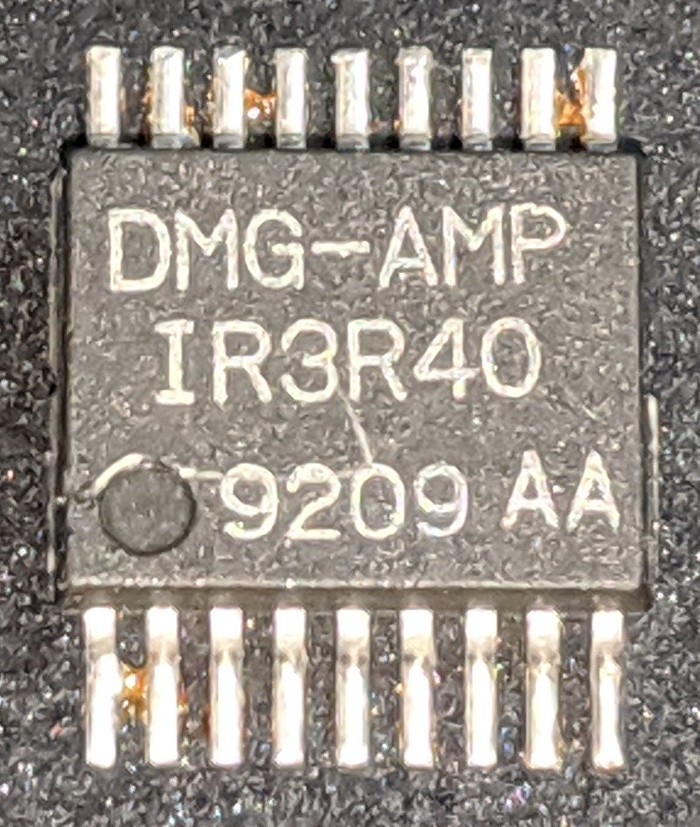
The amplifier chip has the inscription DMG-AMP, which stands for Dot Matrix Game amplifier. The part number of this 18-pin chip from Sharp) is IR3R40.
The internal designation of the chip is SBG14.

At the top left of the chip, there are two large driver transistors for the speaker (one pulls the signal down and the other up). The headphone amplifier consists of two almost identical blocks - for the left and right channels. The circuits of current sources and current mirrors are common for both channels. At the bottom left of the chip is the digital logic that turns on the amplifier for either the speaker or the headphones - it is activated when headphones are connected. Clickable

By carefully examining the crystal, you can find components such as transistors and resistors. And starting from this, you can understand the whole scheme. In the photo above, the white lines are the metal layer of the chip that connects the components. The silicon itself looks greenish and is under the metal. Green rectangles around the perimeter are pads for soldering wires connecting the crystal and 18 contacts of the chip. To change the electrical properties , impurities are introduced into some areas of silicon during the doping process . The next section explains how different components are made from these different types of silicon.
NPN transistor
The amplifier chip uses NPN and PNP bipolar transistors , which are different from the low power MOSFETs used in processors. These transistors have three contacts - an emitter, a base, and a collector. The enlarged photo below shows an NPN transistor. Differing shades of silicon give away areas to which impurities have been added to form the N and P regions. Dark lines separate these areas. The silvery bubbles are a metal layer on top of the silicon that forms the conductors that connect to the base, emitter, and collector.

NPN transistor in the Game Boy Color amplifier chip. Collector C, emitter E, and base B are marked. N and P are silicon regions with impurities.
Below the photo is a vertical sectional diagram describing the device of the transistor. Emitter E connects to silicon N +. Beneath it lies the P layer, which connects to the base pin B. Below it is the N + layer, connected (indirectly) to the collector C. If you look at the vertical section under the letter E, you can see the NPN layers forming the transistor.
Below is another structure used for high output current transistor driving a speaker. They are larger and have many intertwined emitter and base "fingers" surrounded by a large manifold. In the photo of the crystal, you can see two such transistors filling the upper left side of the crystal.

Large high-current NPN transistor in the Game Boy Color amplifier chip. Collector C, emitter E and base B are marked.
PNP transistor
Also, the chip uses completely differently designed PNP transistors. They are described in the diagram below. The most obvious difference is that they are round.
Most of the PNP transistors on this chip are round. However, when combining several PNP transistors, a rectangular structure is still used. Square-wave PNP transistors are larger than square-wave NPN transistors. The chip also has multiple PNP transistors with multiple collectors each. Other PNP transistors do not have dedicated contacts for the collector - instead, a substrate (ground) is used.
A PNP transistor has a small circular emitter (P-silicon) surrounded by a ring-shaped base (N-silicon), which in turn is surrounded by a collector (P-silicon). The emitter metal covers both the emitter and the base, but only connects to the emitter. These patches form a PNP sandwich horizontally (sideways) rather than vertically like an NPN transistor. Although the base portion physically surrounds the emitter, the metal contact with the base is further away. The signal from the base passes through section N under the collector.

PNP transistor on the Game Boy Color amplifier chip. Contacts with collector C, emitter E, and base B, as well as silicon with N and P impurities are noted.
Resistors
Resistors are an important component of an analog chip. The photo below shows long, zig-zagging resistors formed from P strips of silicon, which looks beige in the photo. Its resistance is proportional to the length of the resistor, so resistors with large values zigzag to fit in the available space. Because resistors are relatively large and imprecise, chip designs try to minimize their number. Yet such an analog chip requires many resistors.

Some of the resistors on the Game Boy amplifier chip. In the center, two parallel resistors provide low resistance. Long, sinuous resistors give great resistance.
The photo below shows seven small resistors, but only two in the middle (in parallel) are connected to the circuit. Additional resistors make it possible to make changes by changing the metal layer - much easier than changing silicon. These resistors bias the output transistor, and this appears to be a critical resistance that needs tuning.

Capacitors
There are three large capacitors on this chip, one for each amplifier. The photo below shows one of the capacitors. A capacitor is simply a massive layer of metal separated from the underlying silicon substrate by a thin insulating oxide layer. At the top right in the photo, you can see the connections of the metal conductors and the silicon substrate. In this chip, capacitors are used to ensure the stability of the amplifier. Due to their size, the three capacitors are easy to spot in the photo of the crystal.

LM380
The Game Boy amplifier chip circuitry is very similar to the popular LM380 audio amplifier chip from 1972, so I'll start by reviewing how the LM380 works. The LM380 has non-inverting and non-inverting inputs, as well as an output that amplifies the difference between the inputs a fixed number of times - 50. It looks like an operational amplifier, but the purpose of the LM380 is to amplify audio, and this distinguishes it from an operational amplifier in several ways: a small fixed ratio gain, no negative voltage and other internal implementation.
The diagram below shows the main functional blocks of the LM380. The inputs go to the differential pair circuit (blue). The inputs to the LM380 (or Game Boy amplifier) go to a differential pair (Q3, Q4), but this differential pair is different from the standard op amps. In particular, the emitters receive a varying current, and it is because of this that feedback occurs.
The output from the differential pair (green) is passed through a single transistor amplifier stage, which boosts the gain. The capacitor stabilizes the amplifier, preventing oscillation. Finally, the output stage (magenta) is delivering a lot of current: power transistor Q7 pulls the output up, and Q8 and Q9 pulls down.
The speaker amplifier output stages of the LM380 and Game Boy use a complementary pair of transistors to pull the signal down. The combination of PNP transistor and NPN transistor acts as a higher power PNP transistor, somewhat resembling a composite transistor .
The feedback loop controls the gain of the LM380, holding it at 50. Unlike an operational amplifier, the LM380 feedback network is connected to the internal points of the amplifier, not the input.

LM380 audio amplifier. Diagram based on application notes.
For details on how the LM380 works, see the National Semiconductor Application Note and the Power Audio Amplifier IC LM380 document . A similar LM386 is described in the lectureand other description .
I will now describe the feedback loop of this chip, since the Game Boy chip works on similar principles. The diagram below shows how the feedback loop of the LM380 works without an input. At the top left, the supply voltage VS, passing through R1, creates current I. Transistors Q5 and Q6 form a current mirror: this causes the current going through Q6 to match the current I going through Q5. The current from Q4 to the remaining chip should be approximately 0 (since the remainder of the chip increases it greatly). As a result, it turns out that the current through R2 (created by feedback with the output voltage) should also be I. Since the resistance of R2 is half that of R1, the output voltage should be equal to half the supply voltage. It turns out that the output voltage at rest will be equal to half the supply voltage, which is what was needed.

When connecting the inputs, the feedback loop works as follows. Suppose a voltage ΔV is given to the positive input. The emitter-follower transistors Q3 and Q4 buffer and boost the input, so the same ΔV appears across R3. As a result, a current ∆I flows through the resistor. This increases the current flowing through Q5 to I + ΔI, and thanks to the current mirror, the same current will flow through Q6. Adding all the currents, we get that the current through R2 should be equal to I + 2ΔI. Since R2 is 25 times greater than R3, 2ΔI increases the output voltage to 50ΔV. Therefore, the input voltage is multiplied by 50. The idea behind this is that the feedback loop fixes the multiplication factor to 50.

It seems to me that the best way to understand the LM380 is to think of it as made out of an operational transresistance amplifier (OTRA), a forgotten relative of an operational amplifier. The OTRA works in the same way as an operational amplifier, except that instead of voltage, currents are applied to the two inputs, and the difference between the currents is amplified, giving an output voltage. The two I currents entering the OTRA should be approximately the same, and the input voltages may be different (unlike an op amp).

The diagram above shows the LM380 as an op-amp and feedback loop. Equating the two currents gives V out = V s / 2 + 51V + - 50.5V - , or approximately V out = V s/ 2 + 50 * (V + -V - ). In other words, the output is centered at half the supply voltage and the difference in input voltages is multiplied by a factor of 50. Nobody else has described the LM380 in this way, so I may be wrong - however, so far I do not see errors in this analysis.
Game Boy Audio Chip: Headphone Amplifier

Game Boy board. The audio amplifier chip is in the middle of the right side.
There are three amplifiers on the Game Boy amplifier chip: two identical for the left and right headphone channels, and one more powerful mono amplifier for the speaker. Game Boy headphone amps and speaker amps are different, however both are similar in principle to the LM380.
The diagram below shows the Game Boy headphone amplifier. If you compare it to the LM380 circuitry, you can see the similarities between the LM380 and the headphone amplifier, but there is also a difference. Most of all, it is distinguished by the input stage and the feedback circuit, and the headphone amplifier circuit is essentially identical.
I did not find the exact values of the resistors on the crystal, but if you compare their lengths, they can be roughly determined. Looking at R48, R49, R50 and R51, I calculated that the headphone amplifier ratio is 22. Judging by the resistors R2, R3, R4 and R7, the speaker amplifier ratio is 30, significantly higher than that of the headphones.
The headphone amplifier has three transistors in its amplification stage, as opposed to one in the LM380 - probably for more gain. The output stage of a headphone amplifier is similar but simplified. The PNP / NPN pair pulling down the LM380 output has been replaced with a single PNP transistor. The biggest difference is the amplifier's Control section, which the LM380 doesn't have. This control circuit turns off the headphone amplifier when not inserted, which saves battery power.

Game Boy headphone amplifier circuit. Drawn by me after reverse engineering the crystal.
The photo below shows the left headphone amplifier. The outgoing contact (bottom right, next to part number SBG14) is driven by seven parallel PNP transistors (top left) and seven smaller parallel NPN transistors (center bottom). The capacitor is at the top left of the center. Lots of resistors snake around the crystal.

Left headphone amplifier-on-chip. The right one is its mirror image.
Game Boy audio chip: speaker amplifier
The following diagram shows the Game Boy speaker amplifier. Unlike the two channels of a headphone amplifier, there is only one speaker amplifier, and it produces a mixture of left and right channels. The input stage and feedback are again almost identical to the LM380. The output stage differs slightly. However, the speaker amplifier stage is completely different: it includes a four-transistor differential amplifier stage, which gives much more gain. Although this amplifier stage is very similar to the input stage, it is connected differently and uses an NPN transistor.

The speaker amplifier circuit in the Game Boy amplifier chip
The overall gain of the chip is limited by the feedback loop. The op amp works so that the raw gain is in the order of 100,000, but the feedback reduces it to something more reasonable, like 50. "Extra" gain increases efficiency and reduces distortion. In other words, the Game Boy's extra amp stage, compared to the LM380, won't make it 100 times louder.
In the second amplifying stage, I did not understand a little. It is similar to a differential amplifier, except that a differential amplifier usually has emitters connected, and in this circuit, the collectors are connected.
The chip has pins for decoupling capacitors to reduce the effects of power fluctuations. Headphone amplifiers have external decoupling capacitors, however, for some reason, the speaker amplifier does not have decoupling capacitors (see diagram). It is possible that due to the lack of this capacitor, the speaker has background hum that people are complaining about.
The decoupling capacitor used in the Game Boy (and LM380) chip helps reduce the effects of power fluctuations. Chips often have decoupling capacitors between power and ground, but this decoupling capacitor is a little different. It is connected to a specific point in the feedback loop, which makes it more efficient than a conventional decoupling capacitor.
Comparison with Game Boy Color
I recently covered the reverse engineering of the Game Boy Color amplifier chip, so it will be interesting to compare the two. The Game Boy and Game Boy Color amplifier chips have similar functions. They look similar even at the crystal level. Both have power transistors in the upper left corner of the speaker, control circuits in the lower left corner, and two headphone channels on the right.

Comparison of audio amplifier chips from Game Boy (left) and Game Boy Color (right)
However, it unexpectedly turned out that these chips are implemented in completely different ways. While the Game Boy uses an LM380 style audio amplifier, the Game Boy Color uses power op amps with more complex circuitry. The most important difference is that the Game Boy chip has internal feedback for gain control, while the Game Boy Color also has an external feedback capacitor, which makes it act as a high-pass filter. For more information, see my Game Boy Color Amplifier article and schematic diagram .
Game Boy system collectors spottedthat different versions of the game sound differently. The original Game Boy had a "warm, bass sound" while the Game Boy Color had a "thin" sound with background noise and hum. And it's not just subjective feelings - the differences are visible on the signal graph:

Interestingly, most of the sonic differences can be explained by analyzing the amplifier chips. The Game Boy's output is close to a square wave, however, due to the 100uF decoupling capacitor, the waveform is sagging. The amplifier in Game Boy Color is set up as a high-pass filter, so it produces high-frequency peaks while losing bass sound.
Conclusion
Game Boy from 1989 and Game Boy Color from 1998 use special amplifier chips. By studying the photo of the crystal, you can reverse-engineer their circuits. Chips generally differ from conventional amplifiers in two respects - which explains the need for special chips. First, each chip has three amplifiers: two for the headphone channels, and one for the speaker. Secondly, to save power, the chip has a special circuit that turns off unused amplifiers depending on whether the headphones are plugged in. Reverse engineering of the chips explains most of the differences in sound between Game Boy and Game Boy Color. The Game Boy Color chip implements a high-pass filter, so the sound is thin and lacks the bass of the Game Boy.