Future ASML scanner with high numerical aperture 0.55 (high-NA EUV) worth about $ 300 million Source: ASML presentation
Dutch company ASML is a monopolist in the market of equipment for photolithography in deep ultraviolet (EUV) with a margin of technological leadership for several years before competitors ... Therefore, the delay in the next generation of scanners will not affect the company's profits, sources say Seeking Alpha. On the contrary, ASML will make even more money by selling current generation equipment.
Some experts believe that in the current situation there is no time for upgrades at all. The deficit is so strong that some manufacturers, on the contrary, are resuming the production of microcircuits of the previous generations previously discontinued.
But this is the market situation. In the future, TSMC and Samsung, of course, plan to improve the technological process. The only question was: to implement the following projects on the current equipment with its upgrade to multipatterning (several sequential operations of lithography and etching through several photomasks with a decrease in nodes to 5/3 nm) - or wait for a new EUV system with one template at 3/2 nm.
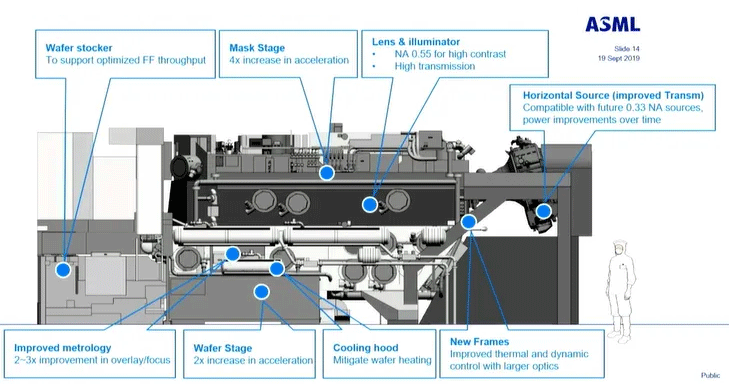
The current instrument for deep ultraviolet lithography is ASML NXE: 3400C, and the next generation high-NA EUV lithography scanner will be ASML EXE: 5000. It will be equipped with completely new 0.55 NA optics, which will significantly reduce the size of the etching elements on the silicon wafer.

How numerical aperture and resolution are calculated are two of the main characteristics of a scanner. Source: ASML presentation
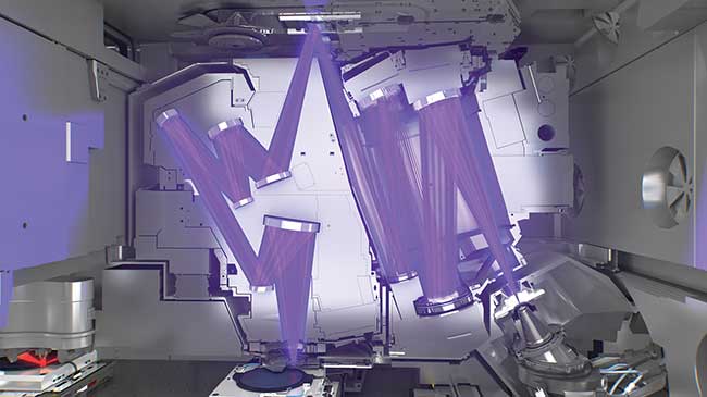
Light pulse path from laser (bottom right) to illumination device, mask with crystal topology through projection optics onto silicon wafer in real ASML scanner.
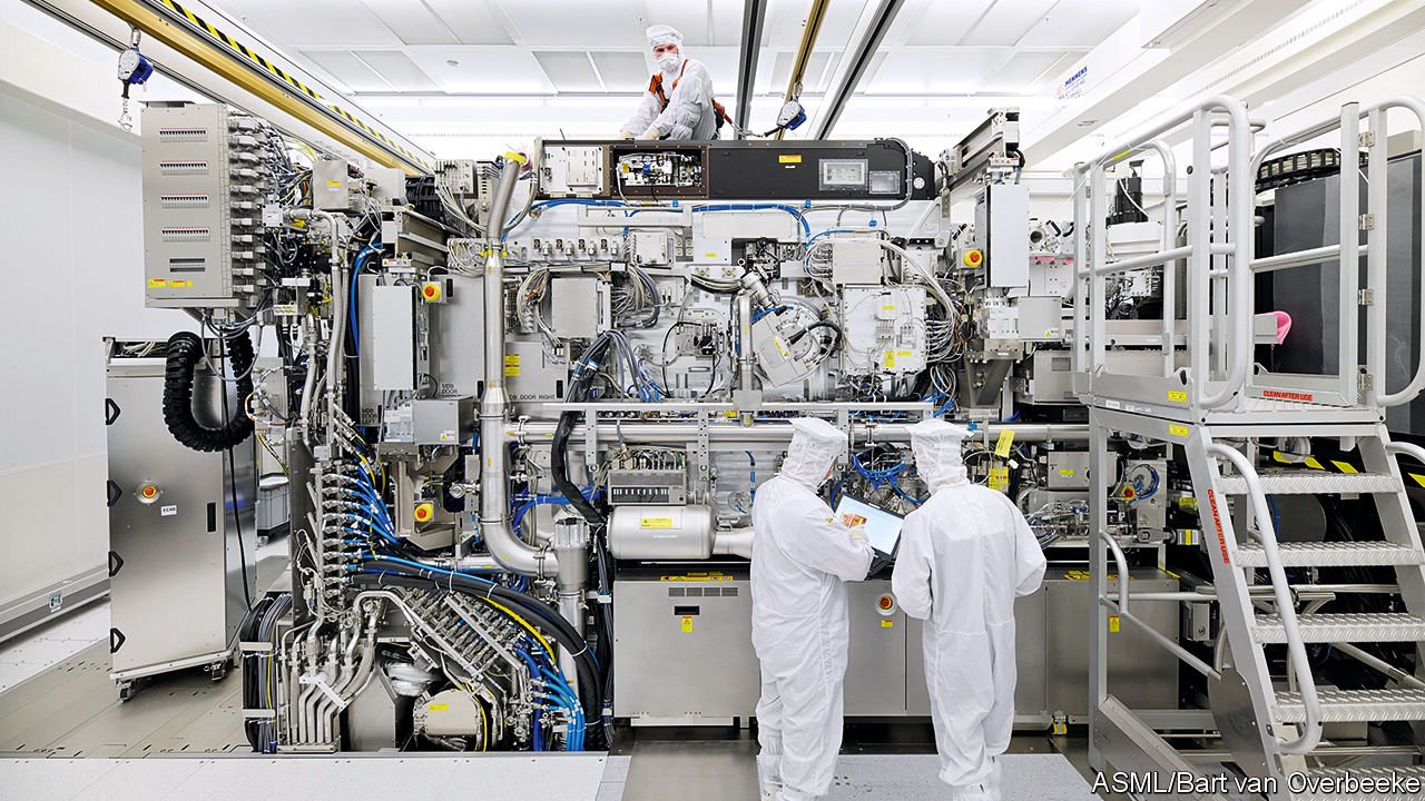
Now the problem is "solved". The transition to new equipment is postponed until 2025 or 2026. These systems turned out to be too complicated and expensive in production, writesSeeking Alpha. As a reminder, the 180-tonne vehicles, the size of a double-decker bus, are in themselves testament to the complex logistics in the electronics industry. The components are manufactured by about 5,000 suppliers. For example, the German Carl Zeiss produces lenses. Dutch VDL - robotic manipulators that feed plates into a machine. The light sources are manufactured by the American company Cymer, bought by ASML in 2013.
Reportedly, one high-NA EUV scanner will cost about $ 300 million (current generation ASML scanners cost about $ 180 million each). Perhaps it will become the most expensive industrial appliance in the global economy.
There is absolutely nothing wrong with the latency of ASML EXE: 5000 scanners. Microcircuits of 3 nm could be produced on new equipment, but now, perhaps, they will be made on old scanners - in several passes and using other architectures. And next-generation scanners will use 2nm chips.
Current EUV equipment for 7 and 5 nm chips uses a 0.33 NA optical system and one to two lithographic exposures. At one point, the double pass seemed easy. Now there are growing concerns that the EUV dual pattern is too complex and expensive for many devices. And at 3 nm, a triple pass may be required, which is even more difficult.
Photolithography in deep ultraviolet
Over the years, chip manufacturers have systematically reduced node size by 30% per generation, thereby reducing the cost of each transistor. In turn, this made it possible to produce more powerful processors. The cycle ticked steadily about every 18 months.
Manufacturing was straightforward until the 20nm mark when the flat transistors hit the wall. Beginning in 2011, chip makers switched to 22nm and 16/14nm vertical gate transistors (FinFETs).
FinFETs are faster and require less power, but are difficult and expensive to make. Thus, the transition time to new nodes increased from 18 months to 2.5 years.
Lithography also faced difficulties. The lithography process begins with a photomask.
Photomask
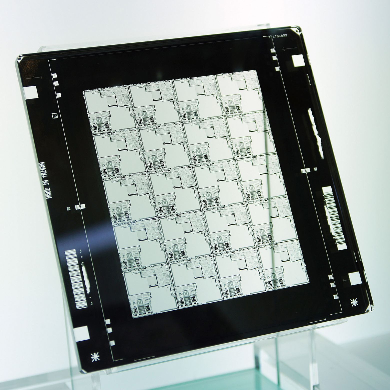
At the factory, the photomask is placed in the scanner. He projects light through the mask onto a plate, creating patterns on it, which are then etched away with acid. This is a simple process with a step size of 28 nm, but already from 20 nm, the parts become too dense, which makes it difficult to print individual elements on the wafer.

Realistic photomask with optical proximity correction. Author: LithoGuy
Therefore, chip makers switched to multipatterning, where the original design is divided into two or more "sparse" photomasks. To apply these elements to the wafer, chip manufacturers use a variety of process designs at the factory, including self-aligned spacer and double patterning.
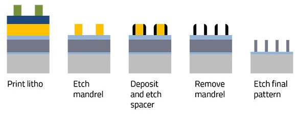
Self-aligning spacers prevent the mask from shifting. Source: Lam Research

Double structuring increases density. Source: Lam Research
The most advanced ASML scanner NXE: 3400C uses a 13.5 nm wavelength and a 0.33 NA optical system. The 246 watt power supply delivers 170 wafers per hour (WPH) throughput.
Samsung, TSMC and Intel are gradually moving to 7 and 5 nm technology nodes using ASML NXE: 3400C scanners. According to the available information , in the 7 nm process technology, one pass with a 40 nm step is enough, but already in 5-nm chips, the same TSMC uses a 30 nm step, which is close to the physical limit at this aperture.
What is high-NA?
Although double crosslinking is still possible for 5 or even 3 nm, this is the limit for vertical gate semiconductors. Next, you need to master nanosheet transistors (nanosheet FET).


Nanosheet transistors
New ASML scanners with a high numerical aperture (high-NA), allowing to increase the image resolution on a photomask, are indispensable.
ASML announced at the January reporting conference that it was delaying the implementation of the new version of EUV for at least three years. Previously, it was planned to master the technology by 2023, and now plans are postponed until 2025 or 2026.
According to experts, a number of technology improvements are required to master the high-NA process technology. The industry is working on them, but there are several unknown factors here.
In recent years, chip makers have worked in parallel on other chip packaging architectures (2.5D, 3D-IC, etc.) to further scale chips even in the event of high-NA latency.
By the way, the current high-NA delay is reminiscent of how the industry has been stuck on 193nm immersion lithography for a long time, which ultimately boosted equipment sales. So from the point of view of the ASML business, there are no problems at all: the company will make more money on the first generation EUV. It also entered the market with long delays, and nothing terrible happened.
The introduction of ASML NXE: 3400C scanners began in 2020. Of the three leading manufacturers, TSMC, Samsung and Intel, the first two are leading in the use of the latest ASML equipment for deep ultraviolet photolithography, and Intel plans to switch to EUV lithography only at the end of 2022.