
Complicated tie
Background ...
As part of my work on reverse engineering of electronic eInk price tags, I encountered an interesting problem. A specific company (Samsung Electro Mechanics / SoluM) switched from using third-party chips, the origin of which I was able to identify (Marvell 88MZ100) to a new chip, which it began to use with its next generation price tags.
It seemed that this is their own chip, developed by the company for this very purpose. Taking on the reverse engineering of such a thing is a dead issue. A friend gave me some price tags with such chips - to tinker. It turned out that they are of two types: one with a segmented display on e-ink, and the other with a conventional graphic display on e-ink. The main chip in both models is the same, so the first thing I did was with a segmented display device, since it is simpler and it is easier to deal with an unknown system using it. It was not entirely clear where to start, but, of course, these are the tasks that are always the most interesting!
Study
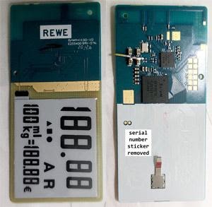
It is foolish to try to solve a crossword puzzle without reading the questions to it. It is just as foolish to reverse engineer a device without first collecting all the information that is already available about it. So what do we initially know? The wireless data transfer protocol is probably the same as usual, since no company wants to migrate to a new one or support two protocols for its customers at once, slowly performing the migration. The old protocol was 2.4 GHz ZigBee-like, so the new one is probably the same. Here is a photo of the board from both sides.
So what do we see? First, a cool example of cost optimization. They laminated the e-ink screen right onto the PCB! Who needs a conductive glass back panel when there is a PCB? The front panel is made of conductive plastic. But it is not important.
Two antennas are visible, both, judging by their size - at 2.4 GHz. As expected, since the previous generation devices also had two 2.4 GHz antennas. We see two chips. Big and small. The large one (designated "SEM9010") apparently has a lot of contacts going to the display and none to the antennas. Obviously this is a display controller.
The small (designated "SEM9110") appears to be the brain responsible for all operations. It is connected to the antennas, the timing crystal, and key points that are obvious here for factory programming.
There are 12 pads here: one is connected to the positive terminal of the battery, one to ground, the purpose of the other 10 is a mystery. Searching for the name of the chip online, I do not find anything useful - definitely their own development. But who designs their own chip for such a simple application? Maybe just a rebranding? Harnessed, we are working!
Curiously, Google Image Search helped here. It happens that this tool comes in handy for reverse engineering. In this case, he leads us to this nugget. (archived copy here for posterity). This is a question from StackExchange - wondering how these electronic shelf labels work. The question is interesting because in the photo posted here, the printed circuit board looks almost identical to ours. The chips are also exactly the same, but the labels on them are different! The board was probably made before SoluM started rebranding these chips.
The chip that I assumed to be the display controller is labeled
SSD1623L2
. Indeed, it is an e-ink segmented display controller that supports up to 96 segments. Searching online, I find the pre-release version 0.1 datasheet (archived copy here for posterity). It's good! If they knew how to get through to this, they could pick up a code that it understands, and as soon as we see this code, that's all!
It turns out that the main microcontroller is
ZBS242
. Okay. I am not familiar with this microcontroller. Let's search the Internet a little more - and the searches lead us to the link (archive copy here for posterity), which also mentions the same answer from StackExchange. The page is Korean, but it shows that this chip has an 8051 core, as well as a fairly predictable peripheral equipment: UART, SPI, I2C, ADC, DAC, comparator, temperature sensor, 5-channel PWM, 3-ch triac controller, IR transmitter, key scan function, RF-Wake function, antenna spacing, ZigBiee compatible radio and MAC. The picture shows that there is also an internal 32 kHz RC oscillator, which, as stated, can consume as little as 1 uA in sleep mode. I think it was this company that made our chip for Samsung. Interesting ...
Let's look at the pictures and find that the SEM9110 crystal that puzzled us was also shot point-blank (archive copy here for posterity). It is stated to be ZBS243. I guess that means there is a whole family of chips here: the ZBS24x. Really interesting.
We have a thread!

Having opened another segment tag, we continue to rejoice in the news: the programming head is signed in clear, legible gold letters! The head appears to have an SPI, UART, reset pin, power supply, ground, and a pin called “test”, probably used to enter factory test mode. Everything is more curious and curious.

It is logical that the oldest representative of the hypothetical ZBS24x family will be designated "ZBS240". Maybe a search for such a query will give us something interesting? Searching for "ZBS240" and filtering out the slag, we find another interesting page in Korean (archived copy here for posterity). It looks like this company makes custom on-demand group programmers. Having looked around on their website, we find a manual (archive copy here for posterity) on their programming device, and we can even download a utility for a PC to work with such a device. This utility even has a tool to update the firmware on the device. I looked to see if it was possible to guess from this information how to program the device, but the firmware turned out to be encrypted. Apparently the PC-side utility is just sending data over the USB serial port, so there is no useful information here either. Sad ...
After searching a little more, we find an even more interesting page (archived copy here for posterity). What is it? Is it on sale?!? Definitely not anymore, right? I just wrote to this company for soap, just in case. Silence ... As a gesture of despair, I asked a friend from Hong Kong if he knew anyone in Korea who could contact these guys, since their website shows that they only accept a transfer from a Korean bank as payment. I was just amazed when he knocked back and said, indeed, he could get me this device through an intermediary found in Korea! A few days later, the device was delivered by DHL!
You can reach him!
How to contact him
Works! I can read the chip and write to it. It took me a while to research the programming tool. Apparently, the chip has 64KB of flash memory and a 1KB "information block", which I believe is used to store calibration values, MAC addresses, and the like. I was able to intercept some of the traces, armed with the wonderful Saleae Logic logic analyzer , watching the programmer do its job. You can download my findings here . In this archive you will find traces of reading, erasing and writing to the INFOBLOCK and CODE spaces. In fact, the protocol is VERY simple! The clock frequency can be anything from 100 kHz to 8 MHz.
ISP protocol: cut to the bone
It all starts with setting the lines to the desired state: SCLK bottom, MOSI top, RESET top, SS top. This condition is maintained for 20 ms. Then RESET goes down by 32 ms. Then at least 4 processor clocks are sent to the SCK line at 500 kHz. Then there is another 10 ms delay until RESET is pushed up. You can now set a delay of 100 ms before starting communication. After that, any number of transactions can be made. A few basic rules: there must be at least 5us between SS going down and sending a byte, at least 2us between the end of the byte and SS going up, and the shortest period that SS can spend up is 2.5us. Therefore, each byte is sent in the state: SS is low, a byte is sent in SPI mode 0, SS is up. Yes of course,SS flips for each byte.
All transactions are three to four bytes long. The first byte indicates the type of transaction, the lowest bit specifies the direction of the transaction: zero means writing to the device, one means reading from the device. The
0x02
/ commands
0x03
are used to initiate communication sessions. The programmer sends a three-byte write:
02 BA A5
and then reads, first sending the read command and "address":, the
03 BA
master sends
FF
while receiving
A5
. If this works, then communication is established.
Commands
0x12
/
0x13
are used to read / write special purpose registers (SFRs) in the CPU (I found this more difficult, but in this case the order is not so important). To select INFOBLOCK, SFR
0xD8
must be set to
0x80
, to select the main flash area, it must be set to
0x00
. To write the value of vv to register rr, SPI data is needed
12 rr vv
. To make sure that the value has been read, it can be read back by first sending a read command and an "address":,
13 rr
after which the master sends
FF
while receiving
vv
.
It is easy to read the flash memory. To do this, apply
0x09
, a four-byte command. After the command byte, the address is sent, first the high byte, then the low. Then the master sends
FF
, in the meantime receiving the byte that has been read. Well yes. A separate command is required to read each byte. Writing is easy too. For this, the command is used
0x08
. This is a four-byte command. After the command byte, the address is sent, first the high byte, then the low byte, and then the byte to be written. A separate command is also required to write each byte. Be sure to erase before recording. To erase INFOBLOCK, it requires only one 4-byte sequence:
48 00 00 00
. Erasing in the main flash memory is carried out using the command
88 00 00 00
.
So now you know enough to trivially program your ZBS24x!
Get to work!

Primer for 8051
If you are already familiar with the 8051, you can safely skip this section.
The 8051 is an old microcontroller designed by intel back in antiquity . It is a terrible hassle to work with, but it is still used quite often because it is cheap to license (in fact, it is free). What's the trouble? The 8051 has several separate memory spaces.
CODE
- This is the area of memory allocated for the code. Its maximum size is 64KB (16-bit address). In the most modern designs, this is flash memory. The code can read bytes from here using a special instruction
movc
("MOVe from Code").
XRAM
Is "external" memory. That is, external to the core. You can store various things in it, but it is almost useless for anything else. Like this: the only operations that can be performed in this memory are writing and reading. Its maximum size is 64KB (16-bit address). How does the address memory of an 8-bit address with a 16-bit wide address work? It turns out to be very slow. The command
movx
("MOVe to / from eXternal") accesses this type of memory, but how do you specify a 16-bit address? For this, a special register called
DPTR
("Data PoinTeR") is used, as well as for working with an instruction
movc
.
DPTR
consists of an upper register
DPH
and a lower register
DPL
... Consequently, by writing to each of them half the address, you can address the external memory and the code memory. As you might guess, this process quickly starts to slip, since, for example, to copy a section from external memory to external memory, you will need to repeatedly shuffle the values between
DPL
and
DPH
. For this reason, some of the more advanced versions of the 8051 have many registers
DPTR
, but not all, and not all of them are implemented the same way.
Intel has added a faster way to access a subset of external memory. In this case, the idea is to use registers
R0
and
R1
as pointer registers. But they are 8 bits in size, where does the other 8 bits in the address come from? They are from a register
P2
(which also controls port 2 for the GPIO pins). Obviously, this practice gets in the way of using port 2 for ... you know ... GPIO. There are ways to smooth out this situation, but I'm not talking about that now. Thus, the amount of memory available to us is limited to 256 bytes (unless you dynamically change port 2, which you probably do not want to do). Usually this memory is called
PDATA
. Similar memory accesses are also done using an instruction
movx
. Next in line we have
SFR
- various configuration registers with which peripherals are configured. This memory area can only be accessed directly. This is the situation: the address must be encoded directly in the instruction, there will be no access through any pointer register. There are 128 bytes
SFR
. The following table shows the lists
SFR
available in accordance with the 8051 standard. The gray boxes contain
SFR
which bits can be accessed individually using bit-wise commands. This is useful when assigning port pins atomic, or when activating / deactivating interrupt sources, or when checking some statuses.
The internal memory on the 8051 is a little tricky. On all modern 8051s, it is 256 bytes. The last 128 bytes
0x80-0xff
are available only indirectly through the registers
R0
and
R1
, but, unlike the situation with external memory, now not only read and write are available to us. We can do an increase by one (
inc
rement), lower by one (
dec
rement), addition (
add
), and most of the other expected operations. In fact, ALL of the internal RAM is accessed indirectly through these pointer registers. Lowest 128 bytes
0x00-0x7f
also available directly (the address is directly encoded in the instruction itself, just like when working with
SFR
. 16 bytes of memory in the range are
0x20-0x2f
also bit addressable using bitwise processing instructions. It is convenient to store variables for boolean values in this part. The lowest 32 bytes
0x00-0x1f
make up 4 banks registers
R0
...
R7
In the status register
PSW
there are bits that allow you to select which bank is currently being used, but in reality, since there is usually a shortage in the internal area with memory, the code mostly uses only one bank of memory.
The 8051 is a machine primarily designed to work with a single operand. That is: in most operations, the battery is used as one of the sources and, possibly, as the destination. Registers can also be used for many (but not all) operations, and some operations allow indirect access to internal RAM, as described above. The stack is an empty upstream, addressable
SFR
, it is called
sp
and is located only in the internal RAM, its maximum size is limited to 256 bytes, but in reality it is much smaller.
Any 8051 ROM image starts with a vector table that contains jumps to the initial code that you want to run as well as the interrupt handlers. In 8051, historically, the reset vector is located at
0x0000
, and interrupt handlers start at the address
0x0003
and then every 8 bytes. Since the instruction
reti
is only used to return from interrupts, it can be used to easily detect whether a particular function is an interrupt handler.
Fill your C compiler channel with all of this and take a puff!
A suitable C compiler for this architecture exists: Keil's C51. But it's not cheap. There is also an open source compiler: SDCC . It's so-so, but free. While doing this project, I found only two great bugs in it, which could only be overcome by bypassing; it's not bad at all for an open source project.
Let's start the analysis
void prvTxBitbang(u8 val)
                  __naked {
  __asm__(
    "  setb  PSW.5       \n"
    "  jbc   _EA, 00004$ \n"
    "  clr   PSW.5       \n"
    "00004$:             \n"
    "  clr   C           \n"
    "  mov   A, DPL      \n"
    "  rlc   A           \n"
    "  mov   DPL, A      \n"
    "  mov   A, #0xff    \n"
    "  rlc   A           \n"
    "  mov   DPH, A      \n"
    "  mov   B, #11      \n"
    "00001$:             \n"
    "  mov   A, DPH      \n"
    "  rrc   A           \n"
    "  mov   DPH, A      \n"
    "  mov   A, DPL      \n"
    "  rrc   A           \n"
    "  mov   DPL, A      \n"
    "  jnc   00002$      \n"
    "  setb  _P1_0       \n"
    "  sjmp  00003$      \n"
    "00002$:             \n"
    "  clr   _P1_0       \n"
    "  nop               \n"
    "  nop               \n"
    "00003$:             \n"
    "  nop               \n"
    "  nop               \n"
    "  nop               \n"
    "  djnz  B, 00001$   \n"
    "  mov   C, PSW.5    \n"
    "  mov   _EA, C      \n"
    "  ret               \n"
  );  }
It's easy to start with the GPIO configuration. As a rule, you will come across several matching bits, which will be set or erased in several registers in a row. This is logical, since when activating or deactivating, you usually have to use the pin as a function (from the GPIO), set it as an input or output, and set or read its value. You should come across this kind of code at the very beginning of work. Let's see what's there ... we find that the standard registers
P0
,
P1
and
P2
actually used that way, how to deal with registers GPIO. By looking at which registers are written around them and what then happens to the bits in them (whether they are read (input) or write (output)), we can assume that the registers
AD
,
AE
,
AF
Are designed to "the function" - and it appears that GPIO, which are set corresponding bits are not used as gpio, and all GPIO, actually used as a GPIO, start working so only after a corresponding bit in one of these registers will be cleared. I named them
PxFUNC
where x is the port number. Then we can conclude that
B9
,
BA
,
BB
control the direction. Whenever a bit is set in one of them, the corresponding GPIO is only read, and when the bit is cleared, the corresponding GPIO is write-only. Hence, we understand that these registers control the direction of the GPIO. I named them
PxDIR
where x is the port number. So now, in theory, I could control the GPIO. If only I knew which of them do what ...
I decided to just try all of them in a row until I find the one that controls the "TEST pad" on the programming head, or maybe the URX and UTX pads. Anyway, actually ... I found that port 1 pin 0 (
P1.0
) is "TEST",
P0.6
this is "UTX", and
P0.7
this is "URX". Having a controlled GPIO, you can simplify your life, but only as long as you can handle debugging by switching different GPIOs, and until you get tired of it. I had time to practice this!
We have printf!
I used this function to turn the "TEST" pad into a regular 8n1 serial port using the bit-bang method, and collected the output using my logic analyzer. I fiddled with it until it gave the baud rate that my USB to serial adapter cable could handle. I already had an 8051 implementation of printf in assembler. For an hour, I practiced outputting complex debug lines from this impromptu serial port. Not a bad start, definitely, this is the only way you need to act in order to move forward effectively!
At this point, I have displayed in the window the values of all
SFR
, to at least navigate what these values are. There were still some problems with further research. To begin with, the watchdog timer (WDT) seemed to only be set by default and reset the chip after one second of execution, so all my experiments had to fit in a second or less. I didn't know how to operate WDT yet, so I put up with this limitation for a while. Be that as it may, one second is many cycles!
Expanding access
Now that I was able to reliably execute the code and output the results, I decided to figure out where the tick controls are. Almost all registers have at least one register that controls different speeds (at least the speed of the CPU) and another register that controls the clock rate (or reset) of various modules. They are usually found like this: the first is usually recorded VERY early at the initial load, and after that it is hardly touched (if at all). The second usually has a bit set (clock cycles) or a bit cleared before we start configuring a peripheral. We do not know where the various peripherals are configured, but usually the set
SFR
with similar numbers corresponds to a peripheral device. So let's see. Definitely there is a case, fit this description:
B7
. We see that one bit at a time is set in it, before several
SFR
with similar numbers are written , and the bits in it will be cleared after calls to several
SFR
with similar numbers stop. We also see that it is initially recorded as
0x2F
, so here we are dealing with peripherals that are included in advance. Since the bits appear to be set prior to what we regard as initializing peripherals, I will call this register
CLKEN
... I fiddled with changing the bits in this register, and it seemed like nothing happened when they were cleared. In principle, this is logical, since I do not use any peripherals.
Another register written nearby (literate code usually initializes all clock operations together), which is then not rewritten, is this
8E
. He writes to
0x21
. I suggested that it might be related to speed. I experimented. Apparently, the 4 least significant bits are not reflected in any way at work, so I have no idea why they are set in
0b0001
, but the next three bits, probably, change the CPU speed quite significantly (as far as I can judge from the speed of my UART, subjected to the drift). The most significant bit seemed to change the frequency a little, I assumed that it is responsible for switching between the internal RC circuit and the external crystal. Three bits, which I assumed worked as a frequency divider, set the clock speed to appear to be equal
16M / (1 + )
. I named this register
CLKSPEED
. Consequently, the highest speed is achieved at the value
0x01
, and the lowest at
0xf1
Making Timers Work
Many manufacturers build on all sorts of things in the 8051, so there is very little standardization here. However, most do not touch the 8051's normal equipment, such as timer 0 and timer 1. Please note: this is not a rule of thumb. For example, TI significantly changes the timers in its CC series chips. I noticed that in this chip, the registers that are normally supposed to configure standard 8051 timers seem to happen close, and interrupt handler # 1 seems to affect them as well. Is it possible to? Standard timers? I tried it and ... it worked. Completely standard, seemingly exactly the same as the original specification. I checked the register
CLKEN
and found that bit 0 (mask
0x01
) to make the timers work. Confirmed that the standard register
IEN0
also works as expected, and that numbers 1 and 3 actually drive interrupts for Timer 0 and Timer 1! The timers appear to be running at exactly 1 / 12th of 16MHz, exactly as would be expected in a standard 8051 operating at 16MHz. So far, I have not found how to change this frequency. What we know now reveals registers
TL0
,
TH0
,
TL1
,
TH1
,
TMOD
,
TCON
! We now have working precision timers!
I was not too lazy to check if the 8052 standard (sequel to 8051) actually implements timer 2. No, it is not.
Or maybe UART?
void uartInit(void) {
    //
    CLKEN |= 0x20;

    //
    P0FUNC |= (1 << 6) | (1 << 7);
    P0DIR &=~ (1 << 6);
    P0DIR |= (1 << 7);

    //
    UARTBRGH = 0x00;
    UARTBRGL = 0x89;
    UARTSTA = 0x12;
}

void uartTx(u8 ch) {
    while (UARTSTA_1));
    UARTSTA_1 = 0;
    UARTBUF = ch;
}
There were several lines in the OTA module. It makes sense that they should relate to something, right? Maybe a debug serial port? This would go well with a board that has the "UTX" and "URX" keypoints. This code was a little convoluted, but it looked like it was storing bytes in some kind of buffer. The code definitely looked like a standard ring buffer. I looked where this buffer is being read. It turned out to be in the handler for interrupt # 0. Oooh, interesting. Could it be a UART interrupt handler? The code seemed to be checking bit # 1 in an area that resembled a status register (register
98
), and if it was set, it read a byte from our ring buffer and wrote it to a register
99
... If another bit (# 0) was set in the aforementioned status register, then it read the register
99
and inserted the result into ... another circular buffer. Well, this is pretty damn in line with what I would expect from a UART interrupt handler! What do we do next?
Each circular buffer has two pointers, one for reading and one for writing. It makes sense that they should be initialized before the buffer is used for anything. So if we find where these indices are initialized, then we will probably find where the UART is installed, right? Definitely looks like this. In that function, which initializes the UART, we see that GPIO
P0.6
and
P0.7
set in function mode,
P0.7
is put on input, and
P0.6
- on output. Two more registers:
9A
and
9B
are are written with
0x00
and,
0x89
respectively. The register that, according to my version, works with states (register
98
) is written as
0x10
, and then bits 0 and 1 in it are cleared. Then
CLKEN
bit 5 is set in , and
IEN0
bit 0 is set in . That's, in principle, all we need!
So we name the register and the register becomes . We know that
99
UARTBUF
98
UARTSTA
UARTSTA
must be set to 0x10 for this block to work, and we know that bit 0 means the UART has a free byte in the TX FIFO queue, and bit 1 means that the UART has a byte for us in the RX FIFO queue. We know that
CLKEN
bit 5 enabled the clock for the UART and that interrupt number 0 corresponds to the UART interrupt handler. It's just a treasure trove of information. Knowing this, I was able to make a working UART driver in my code and send an outgoing message to the desired "UTX" pin, which, as we now know, is located at port 0 pin 6 (
P0.6
). We also learned that the "URX" key point is connected to
P0.7
, and that this is the RX line in the UART. The UART was sending data at 115,200 bps, 8n1, and was in no way affected by the register
CLKSPEED
... So what are these two other mysterious registers that give these magical meanings?
I tried to tinker with the two remaining registers,
9A
and
9B
. It quickly became clear what they were for. These are frequency dividers. I substituted a few values to see how they affect the baud rate. It turned out to be simple.
9A
(hereinafter referred to as
UARTBRGL
) was the low byte, and
9B
(hereinafter referred to as
UARTBRGH
) was the high byte (the upper 4 bits are apparently ignored). The baud rate is calculated simply as
16M / (UARTBRGH:UARTBRGL + 1)
. This perfectly explains the values that seemed magical - they correspond to 115,200 baud.
Apparently, a small bug is related to the fact that the status bits can be cleared programmatically without affecting the FIFO, so if you accidentally clear the bit that means "there is free space in the TX FIFO" (
UARTSTA
.1), then the interrupt will never occur, and the bit will stay low.
Curiously, these locations match the correct 8051 addresses for
SCON
and
SBUF
, which are the 8051 serial port registers. Bits 0, 1, and 2 in
UARTSTA
really fit the descriptions
SCON
from 8051, but that’s where the similarity is over. UART from 8051 requires bits 7 and 6 to be set
SCON
in 0 and 1, only in this way it will become a normal UART. This chip in this case requires 0 and 0. Moreover, the 8051 UART usually does not have a baud divider, instead of which timer 1 is used.
Watchdog timer and "look!"
By this point, the 1 second execution limit guaranteed by the default watchdog configuration was beginning to annoy me. I decided to find out where and how the watchdog is configured. Typically, the watchdog timer is configured as part of its own function, and it is small. Of course, I will not say that this always happens, but most often it looks like this. I had several candidates, and I tried to copy from each in turn the writes of registers into my test program, but the watchdog did not give way. I needed to properly reset the chip every second.
While doing just that, I noticed a very strange function. Apparently, she read the register under the number
FF
, wrote something there, then reset
P1DIR
, wrote to some other register, and then restored the original value in the register
FF
. The weird thing was that it set ALL pins on port 1 to pin. This is nonsense. On other models, port 1 has multiple pins configured as input. In addition, such registers are usually operated bit by bit, using instructions
anl
(logical AND) and
orl
(logical OR). Such a rough writing to the entire register at once looked repulsive. What is it about the register
FF
that needs to be backed up and restored? It looked very strange!
I decided to investigate. When dumping the register value to the console
FF
, it turned out to be zero, which, of course, did not suit me. I searched the entire firmware and noticed that almost everywhere in it there is a recording, then a backup, and then the original value is restored. I also noticed that writing almost always happens with a value
0x04
and rarely with
0x00
... This register was read only during backup for further restoration; no other actions were performed on this value. What functionality does this indicate? Basically, this is how memory banking controls usually work! When you have more information than you can fit in your address space, you have to switch. This access pattern (backup before change and then restore) is typical for such practical situations. But what can they store? Could this be? Are these madmen overloading the memory space itself
SFR
?!
I wrote a program that could display the values of all
SFR
, all 128. Then I turned the bit
0x04
into
FF
SFR
and again took out all the space
SFR
. Then the program wrapped this bit back and again displayed all the values. God Almighty! And there is! Bit 2 in the register
FF
really saves space
SFR
. I have no doubt seen that when this bit is set, the values that appear change. Apparently, this did not affect ALL addresses
SFR
, but many. I named this register
CFGPAGE
.
Now that
CFGPAGE
I thought I was sorted out, I returned to my mysterious function, which zeroed out
P1DIR
. Already knowing that it is NOT reset to zero in this case
P1DIR
, but his strange cousin on another page
SFR
, I tried to copy this code into my program. Believe it or not, I accidentally stumbled upon a code that disables WDT !!!
Investigated the code surrounding this function, since usually related functions in binaries are located next to each other. There were indeed several functions nearby that also accessed
CFGPAGE
and accessed the adjacent address
P1DIR
. After a few hours of trial and error, I fully understood the details of how the watchdog works. On the 4th page of configurations, the address
BF
appears to control the enable and reset of the watchdog timer; the most significant bit of this register enables or disables the chip reset function in the watchdog timer. I named it
WDTCONF
. Address
BA
(which is
P1DIR
on configuration page 0) is the watchdog timer enable register. Bit 0 here enables or disables the watchdog timer itself. I named it
WDTENA
.
Up to this point, I was still figuring out how to tame the watchdog timer. It took a while, but in the end I figured it out. A register
BB
(now named
WDTPET
) can be written to zero to tame the watchdog timer. It took me a few more minutes to figure out how to configure the delay in the watchdog timer, since there was clearly a hole in the address space between
BB
and
BF
... The counter is 24 bits long and is overloaded when tamed. It cannot be read. Reload value saved in
WDTRSTVALH
:
WDTRSTVALM
:
WDTRSTVALL
, located at
BE
,
BD
,
BC
respectively, on the configuration page 4. The counter counts UP at a frequency of about 62 kHz, and an overflow is triggered. Thus, in order to deliver an increased delay, a smaller value must be written to these reset registers.
More subtle possibilities
Flash memory programming
//    irqs
voif flashDo(void) {
    TRIGGER |= 8;
    while (!(TCON2 & 0x08));

    TCON2 &=~ 0x48;
    SETTINGS &=~ 0x10;
}

void flashWrite(u8 pgNo, u16 ofst,
              void *src, u16 len) {
    u8 cfgPg, speed;

    speed = CLKSPEED;
    CLKSPEED = 0x21;
    cfgPg = CFGPAGE;
    CFGPAGE = 4;

    SETTINGS = 0x18;
    FWRTHREE = 3;
    FPGNO = pgNo;
    FWRDSTL = ofst;
    FWRDSTH = ofst >> 8;
    FWRLENL = len - 1;
    FWRLENH = (len - 1) >> 8;
    FWRSRCL = (u8)src;
    FWRSRCH = ((u16)src) >> 8;
    flashDo();

    CFGPAGE = cfgPg;
    CLKSPEED = speed;
}
void flashRead(u8 pgNo, u16 ofst,
    void __xdata *dst, u16 len) {
    u8 pgNo, cfgPg, speed;

    speed = CLKSPEED;
    CLKSPEED = 0x21;
    cfgPg = CFGPAGE;
    CFGPAGE = 4;

    SETTINGS = 0x8;
    FWRTHREE = 3;
    FPGNO = pgNo;
    FWRDSTL = (u8)dst;
    FWRDSTH = ((u16)dst) >> 8;
    FWRSRCL = ofst;
    FWRSRCH = ofst >> 8;
    FWRLENL = len - 1;
    FWRLENH = (len - 1) >> 8;
    flashDo();

    CFGPAGE = cfgPg;
    CLKSPEED = speed;
}
void flashErase(u8 pgNo) {
    u8 __xdata dummy = 0xff;
    u8 cfgPg, speed;

    speed = CLKSPEED;
    CLKSPEED = 0x21;
    cfgPg = CFGPAGE;
    CFGPAGE = 4;

    SETTINGS |= 0x38;
    FWRTHREE = 3;
    FPGNO = pgNo;
    FWRDSTL = 0;
    FWRDSTH = 0;
    FWRLENL = 0;
    FWRLENH = 0;
    FWRSRCL = (u8)&dummy;
    FWRSRCH = ((u16)&dummy) >> 8;
    flashDo();

    CFGPAGE = cfgPg;
    CLKSPEED = speed;
}
I focused on the OTA image as it is smaller than the main firmware. One detail that is definitely needed in the OTA image is the ability to write to flash memory. What does it look like? It is assumed that we need some kind of function that will erase the flash, since the flash is erased in blocks. You also need a write function that can write a page of data or less. We need some kind of verification of the recorded data. The only detail that differs in the implementations is how we will feed the data intended for writing to the flash controller. I didn't know what it should look like, but the rest was easy enough to find. Verification would probably boil down to just calling
memcmp
or cycle. Flash erasing operations wear out the flash memory, so the page must be checked before erasing and then the operation performed.
Looking for a pre-erase check, I quickly found a function that creates a
0x400
byte-to
XRAM
-full area of bytes
0xFF
. Then the memory area is
CODE
compared with this buffer, and if they are not equal, then interrupts are disabled, and some are touched
SFR
on the configuration page 4. The page size in flash memory is clearly 1024 bytes. Checking what other places are affected by the same
SFR
, we find the remaining flash code. It is clear from the context what these registers do and how. In this case, it is interesting how the data is fed to the flash memory control unit. This control block clearly contains a DMA block. An address is supplied to the flash memory control unit
XDATA
and data is absorbed directly from there. How cool!
By that time, I was not yet sure how to read INFOBLOCK. Apparently, the OTA code did not concern him, but from somewhere it MUST be read - after all, there is data in it. I checked the main image and noticed a code snippet affecting the same
SFR
from flash memory, but in a different way. With some more analysis, I was able to reproduce the correct reading of INFOBLOCK. It is curious that the same method can be used to read any other block of flash memory, but there is no need to do this, since all you need to do to read the flash memory is to read the memory area
CODE
. INFOBLOCK is only accessible via the flash memory control unit. For both write and read from flash memory, the control block uses direct memory access (DMA) and writes to
XDATA
.
One register
DF
(
FWRTHREE
) defied any attempts to explain it. It always had a record with the value
0x03
, I do not know why. My flash access code does the same. Register
D8
(
FPGNO
) is written with the flash page number. The main pages of flash memory are numbered from 0 to 63, with INFOBLOCK number 128
DA
.:
D9
(
FWRSRCH
:)
FWRSRCL
is the source of the DMA block in the flash memory control block. For writing to flash, it contains the address
XDATA
where we find the data to write. To read the flash, a byte offset on the original page is looked for, and reading begins at that offset.
DC
:
DB
(
FWRDSTH
:
FWRDSTL
) Is the assignment for DMA in the flash memory management block. For writing to flash, it will contain the byte offset on the destination page, and writing will start from that point. To read the flash, the address is used
XDATA
at which the data received during the read is written.
DE
:
DD
(
FWRLENH
:)
FWRLENL
Is the length of the data that the DMA block should transfer, minus one.
Writing to flash memory as such is triggered by setting a bit in one more
SFR
. Various bits in it are also set to control other code, apparently not related to flash memory, so I concluded that this register would probably initiate various actions. I named this register
D7
on the configuration page 4
TRIGGER
. Completion status is also checked in a register that appears to be shared by other code as well.
CF
I named this register from the configuration page 4
TCON2
, why not? There was also a register on
C7
, also used in conjunction with other code, which apparently configured which operation to perform. I named it
SETTINGS
.
0x30
was written to it with a logical OR to erase + write,
0x18
to write a flash,
0x08
to read a flash. I guessed that the bit
0x08
means "data transfer pending"
0x10
means "in flash", and
0x20
"Erase". This is logical considering what values we see and what operations are performed here.
Reading and writing to the flash worked wonderfully well, but erasing apparently didn't work. Instead of erasing the page with the given code, for some reason, the page on which the code requesting erasure was located was erased all the time. Obviously, this problem was not in the code that was contained on this device, I was doing something wrong. Checked, checked, and checked again to make sure my code matches the factory code. Matched. What's wrong? I worked for several days until I realized that the factory code works at 4MHz, and mine at 16MHz. Could this be the point? It turned out exactly so! I changed my flash erase code to keep the current frequency divider and slowed down the clock to 4MHz for the duration of the flash erase. Went ok as this code is already running with interrupts disabled.
Another subtlety of this flash memory control unit is that it apparently does not provide for a simple "erase" operation. I thought about assigning the appropriate if-bits in the register
SETTINGS
, and then it seemed logical to me that when set to
0x20
or
0x30
, a simple erase should occur. The only way to erase this is to perform an erase + write operation, which writes at least one byte (since there is no way to represent a zero length in
FWRLENH
:.
FWRLENL
To perform a simple erase, I simply ask to write a single byte
0xFF
. It works
SPI
Basically, all SPI drivers are the same. A byte is received at the input, a byte is returned at the output. Of course, some have DMA and some are interrupt driven, but 99% of them in small systems are software controlled, and somewhere there is a simple function
u8 spiByte(u8 byte);
.
It was logical to look further into SPI. Since we know that it
SSD1623L2
communicates with SPI, and we also know the details of organizing such communication, we just need to look at the code and find out which part of it should do this operation. Just like in Sudoku, given how much we already know, this search won't be difficult. Looking at the datasheet
SSD1623L2
we see that the register number of the first sent byte is written in bits 1..6, and the "write" bit is at position # 7. All registers are 24 bits long. It is logical that the programmer will write a code that will take the register number as a parameter, shifting it to the left by one, perhaps logical-or-in
0x80
, if a write is requested, and then transfer three bytes. Not all programmers act logically, but this assumption helps immeasurably in reverse engineering. Looking at the code, it's easy to see the functions that look like they do just that. Some add
0x80
, some don't. They all call that same mysterious function for every byte. So, we assume that some display text on the screen, some read. Let's tackle the mysterious function itself.
In fact, everything is very simple here. It switches
CFGPAGE
to 4, then writes the
ED
value to the register
0x81
, writes the byte to be sent to
EE
, writes
0xA0
to
EC
, makes a delay of 12 microseconds, sets bit 3 to
EB
, reads the received byte from
EF
, stores
0x80
to
ED
. That's all. How to comprehend all this? As before, relying on what is already known.
0x80
and
0x81
differ by only one bit, and we set it before starting the SPI operation, and at the end of the work we reset it, so this is, apparently, an "activating" bit of some kind. On the other hand, the meaning
0xA0
literally sounds like a configuration of some kind. The register
EB
is still a mystery. But, if I reproduce this code without writing to it, everything will work, so I conclude that not much depends on this register. Definitely
EE
this
SPITX
and
EF
this
SPIRX
. I called
ED
-
SPIENA
and
EC
-
SPICFG
.
It remains to characterize what the beats do in
SPICFG
... I did a bit of trial and error, armed with a logic analyzer. Bit 7 must be set, bit 6 must be cleared. Bit 5 starts the transmission of the SPI byte and clears itself when finished with it. Bits 3 and 4 set the clock frequency, you can choose from values: 500KHz, 1MHz, 2MHz, 4MHz. 2 is the standard configuration bit
CPHA
for SPI, bit 1 is
CPOL
. Bit 0 appears to violate RX. I am assuming he can configure the block for half duplex (in line
MOSI
). In general, it is not so difficult.
Pin by pin, quickly find the GPIO configuration and see what
P0.0
this is
SCLK
,
P0.1
this
MOSI
and
P0.2
this
MISO
... By looking for where these GPIOs are configured, we also see how the
CLKEN
SPI bit is needed : that's bit 3. Great - we now have a working SPI!
Determine the temperature
volatile u8 __xdata mTempRet[2];

void TEMP_ISR(void) __interrupt (10)
{
  uint8_t i;

  i = CFGPAGE;
  CFGPAGE = 4;
  mTempRet[0] = TEMPRETH;
  mTempRet[1] = TEMPRETL;
  CFGPAGE = i;
  IEN1 &=~ 0x10;
}

int16_t tempGet(void)
{
  u16 temp, sum = 0;
  u8 i;

  CLKEN |= 0x80;

  i = CFGPAGE;
  CFGPAGE = 4;
  TEMPCFG = 0x81;
  TEMPCAL2 = 0x22;
  TEMPCAL1 = 0x55;
  TEMPCAL4 = 0;
  TEMPCAL3 = 0;
  TEMPCAL6 = 3;
  TEMPCAL5 = 0xff;
  TEMPCFG &=~ 0x08;
  CFGPAGE = i;
  IEN1 &=~ 0x10;

  for (i = 0; i < 9; i++) {

    //
    IEN1 |= 0x10;

    //
    while (IEN1 & 0x10);

    if (i) {  //

      sum += u8Bitswap(mTempRet[0]) << 2;
      if (mTempRet[1] & 1)
        sum += 2;
      if (mTempRet[1] & 2)
        sum += 1;
    }

    timerDelay(TICKS_PER_S / 1000);
  }
  //
  CLKEN &=~ 0x80;

  return sum / 8;
}
E-Ink displays update differently based on the current temperature, so knowing the ambient temperature is critical to update them correctly. The correct waveforms are selected depending on the temperature. Here knowledge from the outside will come in handy. So if we can find where the waveforms are loaded into the display controller, we can find where the choices are made. From this place you can walk directly to the point where the temperature is measured, right? Having done this, we go to exactly one function, the output of which determines which waveform will be used. This must be it! By the way: usually temperature sensors are attached to the ADC - almost no one makes them in a separate version. But it doesn't matter [yet].
It all starts with setting bit 7 to
CLKEN
and ends with its reset, so that at least we know that this is how we turn the temperature sensor (or ADC) on and off. The function switches
CFGPAGE
to 4, then writes a series of values to a series of registers. All values are constant.
0x81
-> reg.
F7
,
0x22
-> reg.
E7
,
0x55
-> reg.
E6
,
0x00
-> reg.
FC
,
0x00
-> reg.
FB
,
0x03
-> reg.
FE
,
0xFF
-> reg.
FD
, then the bits are
0x81
flushed to
F7
. Thereafter
CFGPAGE
recovers and then clears bit 4 in the register
A1
. This seems to be the initial setup. After a certain procedure occurs five times, the results of all operations except the first are averaged. After that, a lot of math is performed on the average obtained in this way, in particular, using the values from INFOBLOCK - these are probably calibration values. The result is then returned. Let's take a closer look at the details.
In the process, bit 4 in the register was simply set
A1
, the global bit was set and then in the active standby mode we spend time until the bit is cleared. The specific averaged values, apparently, are taken from some global one. This is weird ... I looked for where it is written and found it in interrupt # 10 handler. Apparently, this was how bit 4 in the register was cleared
A1
, then the switch to configuration page 4 occurred, the values were read from the registers
F8
and
F9
, and some strange things were done with them, and then this global value was written. But what is done with these values?
I was just in the eyes pricked constants
0x55
,
0xAA
,
0xCC
and
0x33
... Is this possible? Could someone be so blunt that ... well, yes. These are constants for a clever way to reverse the order of the bits in a byte. Tricky, but only on more advanced processors. On 8051, this approach is very ineffective. But why? It seems that whatever IP (command pointer) they license to measure temperature, it produces a result in which the bits are in reverse order. Why this problem should be resolved at the software level of a proprietary chip is a big question. After all, reversing the order of bits in hardware is no more difficult than reordering a few wires ... What does it do? I do not know. In fact, I never got it.
Almost no one designs a dedicated command counter for a temperature sensor, this thing is simply plugged into the ADC. Once I was able to re-implement this code and make sure it worked very well, I tried to change all of these registers. Most of them influenced the gain of the temperature sensor, some had no effect. If this were a normal ADC, we would expect some bits to switch it to a different kind of input and give a completely different value. Unfortunately, this did not happen. It really looked like a normal temperature sensor. This is also confirmed because these registers are not touched anywhere else. Weird as hell, but okay ...
Since almost all of these registers are written only once, and these are the values, and changing them affects the measured value, I decided to simply call them all temperature calibration values. Therefore, we get acquainted with
TEMPCAL1
(reg.
E6
),
TEMPCAL2
(Reg.
E7
),
TEMPCAL3
(Reg.
FB
),
TEMPCAL4
(Reg.
FC
),
TEMPCAL5
(Reg.
FD
) And
TEMPCAL6
(reg.
FE
). I named it since it is used a number of times and seems to actually manage the loading of the calibration value. The results are issued in (reg.
F7
TEMPCFG
TEMPRETH
F8
) and
TEMPRETL
(reg.
F9
). Results are 10 bits in length, aligned to the upper end of a 16-bit result register, with reversed bit order.
I also noticed that bit 3 in is
TEMPCFG
set when the sample finishes creating. Curiously, the factory code doesn't check it, relying instead on the interrupt. But, in fact, it came in handy in deciphering the purpose of the register
A1
. As you can see, the classic 8051 is limited to 7 interrupt sources, since we have 8 bits in the register
IEN
and bit 7 is reserved to activate a global interrupt. So how do you manage interrupts numbered 7 and up? In fact, it’s like the wild west, what you want is what you do. But here we have a hardware element that triggers interrupt number 10, and using a bit, we can determine when it was made. This is great for experimenting. in which we want to know how interrupts above 7 are activated and deactivated. It was just necessary to tinker with this code until you get rid of the interrupt, but the sample is created . The search did not take long. It must be it
A1
! I named him
IEN1
... I'm not sure what the function of bit 0 is here, but bits 1 and above control the activation of interrupts number 7 and above. I was able to confirm this later. So done - we've documented yet another peripheral, thus discovering even more oddities ...
I2C
At this stage, I opened a larger e-Ink price tag equipped with the same chip. It was a 2.9-inch model with an e-ink graphic display and NFC !!! Again, third-party knowledge comes in handy here. Most NFC devices will tell you exactly what they are if you ask politely. This is a good thing, as the NFC chip on the board was too small to be properly labeled. After scanning it using NFC and checking the device ID, we find out that it is NXP NT3H1101 (archived copy here for posterity). From this very convenient page you can download the datasheet - and it immediately becomes clear how communication with this chip should proceed. Helpful information! (All information is useful here). The only annoying thing is that the I2C address of this device is not fixed, but it can be set to any value; however, a default value is provided. The alphabet of reverse engineering: in 99.9% of cases, the default values do not change. I bet the default I2C address hasn't changed either!
Finding a binary analogue for is
0x55
quite easy - this value is not so common. Apparently, they are all made before calls to one of the two functions. It makes sense that they should be connected to I2C. Moreover, in all cases, before these calls, bit 4 is set in
CLKEN
which is then discarded. We now know that I2C is activated through this bit. Let's take a look at what these functions do. Some copy data from the provided parameter at the very beginning, some do it at the end. In the middle, they all write some global stuff, set the global bit, clear bit 4, and set bit 5 in the register
95
and wait for it to be cleared. Hmm, works like a temperature sensor. Apparently bit 2 in the
IEN1
interrupt activates.
Let's see where the interrupt handler that affects these global values is located. Indeed, its interrupt number is 8, as expected. It sets
CFGPAGE
to 0 and then reads the register
91
... The least significant 3 bits are ignored, and the remaining bits are used in the switch-case to decide what to do. This code turned out to be a little confusing, so I decided to experiment. Attached the logic analyzer to the lines going to the NFC chip and quickly found where
SDA
and where
SCL
. It was easy because there is a datasheet for this chip.
It seems that clearing bit 4 in the register
95
will not affect anything, but setting bit 5 causes the START condition on the bus to be true. An interrupt is triggered. If you do the same using the built-in handler and read the 5 most significant bits in the register
91
, we see that they have a value
0x08
... The address byte is then stored with the R / W (read / write)
94
bit in the register , and bit 3 in the register is cleared
95
. It should also be noted that ALL paths through this interrupt handler result in bit 3 being cleared in the register
95
. I guess this is the "bit that needs to be interrupted." I haven't figured it out yet, but we can already name some registers. It seems that all the I2C registers are on config page 0.
I'm going to call because it is I2C that it contains and is never read for any other reason. I have never seen the least significant three bits change or in any way used. - so I will call
91
I2CSTATE
I2CBUF
94
, since the data is pumped through it along the conveyor, and
95
in the future it will be named
I2CCTL
, since in order for things to be done, something needs to be written into it.
We dig further and find that when the address byte is sent, one of four status values can be obtained. If the address byte we sent required write access, then the state will be
0x18
if it was acknowledged (ACK), and
0x20
if not. If the address byte we sent required read access, then the state will be
0x40
if it was acknowledged (ACK), and
0x48
if not. The handling of NAK (byte unacknowledged) is quite straightforward. When bit 5 is set to
I2CCTL
the STOP condition on the bus is true.
Sending data in write mode is easy. The byte is simply written to
I2CBUF
. If the sent byte is acknowledged (ACK), then the state will become,
0x28
and if not, then
0x30
. To provoke a restart, set bit 4 to
I2CCTL
- it works. When the execution of the RESTART command on the bus completes, the state becomes
0x10
.
If we want to read the information, then, after sending the restart bit and the address byte in read mode, as soon as we see the status
0x40
, we can decide how to respond to the next byte we receive - ACK or NAK. To acknowledge it (ACK), set bit 2 to
I2CCTL
, and in order not to confirm (NAK) - we clear this bit. With the return of the handler, the byte will be received. When this is done, we will see the status
0x50
if the byte was confirmed, and
0x58
if it was not confirmed. One way or another, the
I2CBUF
received byte will be contained in.
After reviewing the initialization code and tinkering with our copy, we find that bit 7 in
I2CCTL
controls whether the peripheral device will trigger interrupts. If not, then this register is initialized to
0x43
... I assume this is how the block is configured to operate in master mode. Since I do not have a sample code for the slave mode, I did not investigate this question further, but I am sure that the slave mode is supported. It can be done, but I'm lazy :).
The register
96
also recorded information in the initialization time, and then no longer changes. This correlates well with one bit of information that we still lack - indicating how the clock speed is set. Having experimented with this register (which is now called
I2CSPEED
), we see that it has a complex interdependence with the clock frequency, but after several dozen attempts I came to the following:
rate = 16MHz / ((dividerB ? 10 * (1 + dividerB) : 12) << dividerA)
where dividerA is the three least significant bits
I2CSPEED
and dividerB is the next 4. The most significant bit is apparently not used.
The fact that the initial GPIO setup occurs near the initialization point of the peripheral seems to imply that pins
P1.4
and are important in this case
P1.5
.
Everything worked, but there was one secret. When the interrupt for this block was activated (c
IEN1
), bit 2 was also set in the register
A2
. Since it
IEN1
is located at the address
A1
, I suspect it has to do with an interrupt. I still haven't figured out exactly what it does, and no code other than the initial I2C setup code uses it. I previously named it
I2CUNKNOWN
although it is more likely to be interrupt related than I2C related. Anyway, my code can now perform I2C transactions as a master!
Pin change detection
The price tag firmware woke up when it was scanned with an NFC-enabled device. The onboard NFC chip has a "field detection" pin connected to the main microcontroller. Coincidence? NotI think! There must be a way to detect changes on the pin. It even wakes up the chip from sleep mode (power saving). In addition, it takes some time to draw with electronic ink, and during this wait, the chip should probably continue to sleep. The display will signal the end of drawing by changing the "BUSY" signal. So ... we have two cases in which the CPU must detect a change on a pin and, most likely, we are not talking about an active wait cycle. It would be difficult to find the first described case - I still did not know exactly where this hibernation code is. The second case, on the other hand, was very easy to find - I mean, it was easy to find the code for drawing on the screen. Again, building on existing knowledge is helpful here. I knew,which team is responsible for "refreshing the screen" on virtually all e-ink display chips in existence. I just entered it and saw what would happen. There was a lot of code, many were touched
SFR
... I started experimenting with the few that I saw. Made some educated guesses: All pins should be able to trigger change detection. This is not always the case, but an educated guess is usually drawn. I assumed that whatever configuration registers we were talking about, they would be sequential and work with three ports. I also assumed that changing the pin should provide an interrupt, and not just wake up the device. It makes sense that the number of configuration registers is fairly predictable. For each pin, we need ENABLE, STATUS and, most likely, DIRECTION. In addition, registers related to GPIO change detection are likely to be close to other registers configuring GPIOs.
Based on this, I did some experiments, since I could easily switch at least some of the pins (for example, TEST). Also took some time to see how my current map is developing
SFR
. I have not forgotten to look at the registers
BC
,
BD
and
BE
on the configuration page 0. Several experiments have shown that they control the pullup of each pin. True, I have never seen any configurations that would allow "pulling the pin down". I named them
PxPULL
.
After several experiments, it became clear that there are three registers per port, and they control interrupts when the pin changes.
PxLVLSEL
(
A3
,
A4
,
A4
) selects the desired level (0 = high, 1 = low).
PxINTEN
(
A6
,
A7
,
A9
) Provides change tracking pin at the hardware level.
PxCHSTA
(
AA
,
AB
,
AC
) Stores the detection status (bit set = something has changed). Other experiments showed that the interrupt number when changing the pin is 11. Works well, and I even managed to wake up the chip from power saving mode (more on this below).
Second DPTR
Registers
84
and
85
mysteriously save up amid all swap transactions
CFGPAGE
and keep all 8 bits stored in them. In many variants of the 8051, this is where the second register should be
DPTR
. But, if so, how do you switch to it? Everyone does it differently. I decided to try it. Wrote a program in assembler to reverse each bit in each register in turn and check if writing an integer
DPTR
(special instruction) followed by reading
DPL
and
DPH
(normal access to
SFR
). It is predictable that many of these things cannot be switched so easily without crashing the program. But, having practiced carefully skipping one or the other, I isolated bit 0 in
92
. Well, yes ... That's what he does. As with many 8051s, I named this register
DPS
, which means "data pointer selection". Registers
84
and
85
I named, of course,
DPL1
and
DPH1
.
Other experiments.
Some experiments have shown that the two least significant bits in
PCON
(standby and sleep) work as expected in sleep mode for the 8051 (although sleep in low power mode can be configured as well). I also noted that setting bit 4 is deactivated
XRAM
. This saves some more energy in sleep mode!
Registers in the range
B2
.. are interesting
B6
. They appear to vary depending on the instructions followed in their location. Having carefully considered everything, I realized that
B4
:
B5
it is always up-to-date
PC
!!! Why someone might need it - I don't know. Named them
PCH
and
PCL
... They are read-only. But what about other registers in this range?
B2
and
B3
appears to be associated with conditional jumps. On a long jump (such as when running
ljmp
,
lcall
or
ret
), they seem to store the destination of the jump. With short transitions (such as
sjmp
),
B2
it seems to figure out the displacement. Strange things, but useless, so I didn't go into them any further. I named the rest of the registers
PERFMONx
.
Sleep in energy-saving mode
People are people, and nothing human is alien to them. People love round numbers. I like accuracy, even if I don't need it. This helps a lot with reverse engineering. For example, how do you respond to a constant
0x380000
? None? Perhaps. How about
0x36EE80
? The eyes are already clinging to her. What the hell does that mean? Translate it into decimal system and you see: 3,600,000. Well , this is an hour, expressed in milliseconds. This value can be useful, perhaps, only in the case of a long sleep in an energy-saving mode. I’m tired of counting how many things I “reverse engineered” by relying on constants of this kind that shed light on where the dream is realized!
Here are the constants on this device were passed to the function of interest to me: 1 5000 2 000 5 000 10 000 3 600 000 1 800 000 0xffffffff. It is quite understandable that this is an indication of the duration in milliseconds. The latter is probably a stub for "forever or almost forever."
There was almost no chance of understanding what most registers are doing here, since they are used by code almost exclusively in sleep mode. Some were in
SFR
and some were in space
MMIO
... I was able to copy the code and reproduce it. In particular, I was interested in that the sleep timer can work at two speeds: with a frequency of 32KHz and 1Hz. This is a 24-bit timer, with which the shortest possible sleep lasts about 30 ms, and the longest can last about 194 days! Read more in the SDK.
Radio
Radio usually requires extensive configuration, so
SFR
it is too crowded in a dense space . Most 8051 equipped with radios are used to solve this problem
MMIO
. Memory-mapped I / O in the 8051 is usually just mapped to the address space
XRAM
. Looking diagonally through the code, I realized that the radio on this chip is in
MMIO:df00 — MMIO:dfff
.
RX path
Again, I decided to start with the OTA image. It is small enough to simplify analysis. It soon became clear that the OTA image does not send any radio packets, but only receives them (acknowledgments are automatically sent at the hardware level, which is typical for most ZigBee chips). But it's good! Thanks to this, it is enough for us to analyze only half of the driver, which means that the task is twice as simple as possible!
When I started looking for where the OTA code gets the data, it seemed like there was a buffer queue. What it is: It is a queue containing individual bytes, each of which is a pointer to a list of buffers. The code that seemed to receive packets and process the received packets took the buffer from the queue, processed it, and then put it in another queue. A very simple scheme. One queue stores buffers full of received data, another queue stores empty buffers ready to receive new received data. Clear enough.
Looking around a little, we quickly discover where the queues are accessed in a different way: removing the buffer from the "empty" queue and enqueuing the full ones. This is the handler for interrupt # 5! The interrupt handler itself was quite simple, provided that the bit was set
TCON2.2
, it saved
0xC6
in
MMIO:df48
, dequeued the buffer, copied bytes into it and put it in another queue. But where did he copy the bytes from? Where did you get the length of the copy? Both were taken from the buffer
XRAM
in which he did not write! I have never been able to unravel this mystery.
The search did not end there. Interrupt 4 played a key role. Its handler turned out to be even simpler. He tested bit 5 in
MMIO:dfad
(I'll call it
RADIO_IRQ4_pending
and, if set, it calls a procedure not called anywhere else. This procedure read , checked that the value in it was less than or equal to 128, read , checked that with an increase by one, it would become equal to the previous value. If any of the above was not performed, then it saved in , otherwise configuration page 4 was selected, the first read value was stored in a global variable, which further denoted the length. This value minus one persisted , and the pointer to the buffer from which subsequently copied data stored in : . Then bit 2 was set in .
SFR
FA
MMIO:df98
0xC6
MMIO:df48
D5
D4
D3
TRIGGER
Here, again, knowing the context helps. 127 is the maximum value a valid 802.15.4 packet can have, and this length includes a 2-byte cyclic redundancy check (CRC), but does not include the length of the byte itself. Therefore, my guess is that
FA
this is the resulting length (taking into account the byte length and CRC). I named it
RADIO_GOTLEN
. In such a case, it makes sense that the
MMIO:df48
(now named
RADIO_rxFirstByte
) could be the first byte (length byte) received. With all the remaining registers is clear:
D5
it is the length of the DMA for RX DMA (now called
RADIO_RXLEN
)
D4
:
D3
it is disassembled into parts pointer to the destination RX DMA (
RADIO_RXPTRH
and
RADIO_RXPTRL
respectively).
Then it all worked out. Interrupt number 4 is triggered as soon as the radio receives a packet into the internal buffer. Bit 5 set to
RADIO_IRQ4_pending
(this is now called
RADIO_IRQ4_pending
) tells us that this happened. We proceed with the initial inspection of the packet (making sure that its length is within reasonable limits), and then we run the DMA from the internal buffer to
XRAM
, if all is well. If not, then we write
0xC6
in
MMIO:df48
. Logically, this can be compared to "emptying the RX FIFO", hence this register is now called
RADIO_command
. If everything was fine with the packet and the DMA operation completed, then bit 2 is set in
TCON2
, and interrupt 5 is triggered. Here, again, we write "emptying RX FIFO" to
RADIO_command
. This is useful since we have already pulled the data using the DMA method. Then the data is copied and the job is done!
In most radios, the received cyclic redundancy code is not provided at the higher layers - it is simply checked and returned with a single status bit with a yes or no value. As usual, it is advisable to assume that everything is working "normally". You check - it is really regular. Most ZigBee radios instead report the LQI (Radio Link Quality Indicator) and RSSI (Received Signal Strength Indicator) in these two bytes rather than the CRC. In this model, the radio works in much the same way. Almost. Apparently the first byte is always
0xD0
but the second seems to actually contain the LQI (in the least significant 7 bits) and the CRC status (in bit 7). In fact, it is functionally very similar to how the Chipcon radio works. The command
0xC6
also means "empty RX FIFO" for chipcon radios (now TI)! Many other things are not the same, but the commands are OPPOSITE , and it helped me navigate the other elements of this radio stack!
More about radio
If you look at how the OTA code initiates the radio, you can see that LOTS of registers are touched only once, some values are written in them, which seem to be completely random. Most likely, many of them are gauge. Any register which is written to once (or repeatedly, but the same value is entered) is a calibration register. I'll skip the boring details of the registers involved, but I'll talk about the working initiation code that is in the SDK.
Here, again, we observe how many values are written to the register
RADIO_command
... The recorded values match those that we would expect to see if we worked with the values of the chipcon commands, although we can see some values that are not in the chipcon radio modules. So, either this radio is a rare chipcon bastard, or they both descend from a common ancestor. In any case, this situation helps to understand some more commands issued by them.
Reproducing the initiation code and writing interrupt handlers, like those built into the chip, gives us a working binary that can work for reception and is conducive to experiments. Noticing some more registers that the main firmware writes to, I quickly determined that
MMIO:df88 — MMIO:df8f
this is "my long MAC address", which will be used at the hardware level to filter incoming packets. Similarly,
MMIO:df90 — MMIO:df91
sets the "own PAN ID" for the RX filter. A
MMIO:df92 — MMIO:df93
sets "own short address". This equipment will accept and acknowledge (ACK) any packet sent to our broadcast addresses.
MMIO:dfc0
sets the radio channel in standard 802.15.4 (11..26) numbering.
Since the radio will acknowledge the packets, I was also able to find that the
MMIO:dfc9
transmit strength is being adjusted when adjusting . I think it's about the register setting the TX power. I also noticed that when a channel is set in the main factory firmware, two more registers are written with per-channel values. There is only one such register in the OTA firmware. The one related to RX is called
MMIO:dfcb
, and the related to TX is called
MMIO:dffd
... Easy enough to reproduce and understand. Then it's time to figure out TX!
Let's send some bytes!
After decrypting the data fetch path, I moved the function and register names into my disassembled master image. Looking at what is still unmarked, we can see where TX's path lies. Indeed, there are two more buffer queues here: one full of empty TX buffers ready to use, and the other full of “used up” TX buffers ready to be sent. I found the transfer function very quickly.
In 802.15.4, it is customary to listen to the radio channel before transmitting. This operation is called CCA (Channel Idle Assessment). Before we do anything with the data we are about to send, consider a loop that reads
MMIO:df98
and checking bit 0. If it is set, then the function fails, and the timer is set to retry. I think this is the CCA path. If we see zero in this bit 128 times, then we consider that the channel is free.
The transfer function itself turned out to be depressingly simple: you select configuration page 4, the desired length (not including the length byte or CRC), and everything is written to
CD
. A pointer to a buffer in
XRAM
written in
CA
:
C9
. The buffer starts with a length byte.
RADIO_command
loaded with value
0xCB
. There is no such command in chipcon radios, but I guess it means "load TX FIFO". Then bit 1 is set in
TRIGGER
... I suppose this is how DMA access to the internal TX FIFO radio queue is started. Then
MMIO:dfc8
set to
0xFF
, 255 attempts are made to wait for TX to end, checking that bit 7 in
MMIO:df9b
(now called
RADIO_curRfState
) is set. Then, after a short delay, it is
MMIO:dfc8
set to
0x7F
. Curiously, I have no idea why it is being recorded
MMIO:dfc8
. In my code, I tried to do without it and everything worked fine.
Tails
After experimenting a bit, I discovered some tricks that the factory firmware cannot do. Bit 6 in
RADIO_IRQ4_pending
is set after we "TX" the packet and the acknowledgment delay (ACK) expires. If we actually receive an ACK, then bit 4 will also be set. Therefore, it is easy to determine (1) when we actually sent the packet and (2) whether we received an ACK. Cool!
Also, if bit 4 in
RADIO_IRQ4_pending
is set and bit 5 in is
RADIO_curRfState
not occupied, this means that we are in the process of receiving a packet. We need to select the RSSI manually, for which we read
MMIO:df84
(now
RADIO_currentRSSI
). It has an offset of about 56 dBm.
I also noticed that bit 1 in
TCON2
set upon completion of TX DMA (but not necessarily the TX process itself). Bit 0 in is
TCON2
set when the radio initialization ends.
Unsolved mysteries
ADC / Battery Measurement and AES Encryption Engine
It makes sense that there should be some way to measure the battery voltage, but I haven't found any trace of any similar code. Without code that uses the ADC in this way, the chances of finding this vanishing method are slim. The AES block is, in principle, the same as the ADC. I know there is an AES acceleration block in the chip (needed for ZigBee). But since the actual code doesn't use it, I don't see a way to find it.
miscellanea
Things that we cannot find, but which we do not really care about, since we cannot buy this chip: IR LED controller, PWM unit, DAC. I will leave these things for the reader to exercise on their own.
ZBS242 / 3 Pinouts, Features, SFR, Downloads
Download ZBS24x SDK .

- The shaded cells indicate bitwise addressable registers
- The diagonally shaded registers that are not stocked in the bank
CFGPAGE
- Vertical shaded registers, which, apparently, do not appear on any of the pages at all.
- Empty cells are unknown registers
- Names of RADIO registers begin with the letter "r"

Lessons for a beginner reverse engineer
- Read the materials for at least a few hours or days before starting work.
- - . -, .
- . SPI , I2C , . .
- , – ( ).
- : , . , , .
- , , .
- . - , - . , .
- - . , , .
- , , . , , .
- - . .
- - , , - .
Cloud servers from Macleod are great for hosting websites.
Register using the link above or by clicking on the banner and get a 10% discount for the first month of renting a server of any configuration!