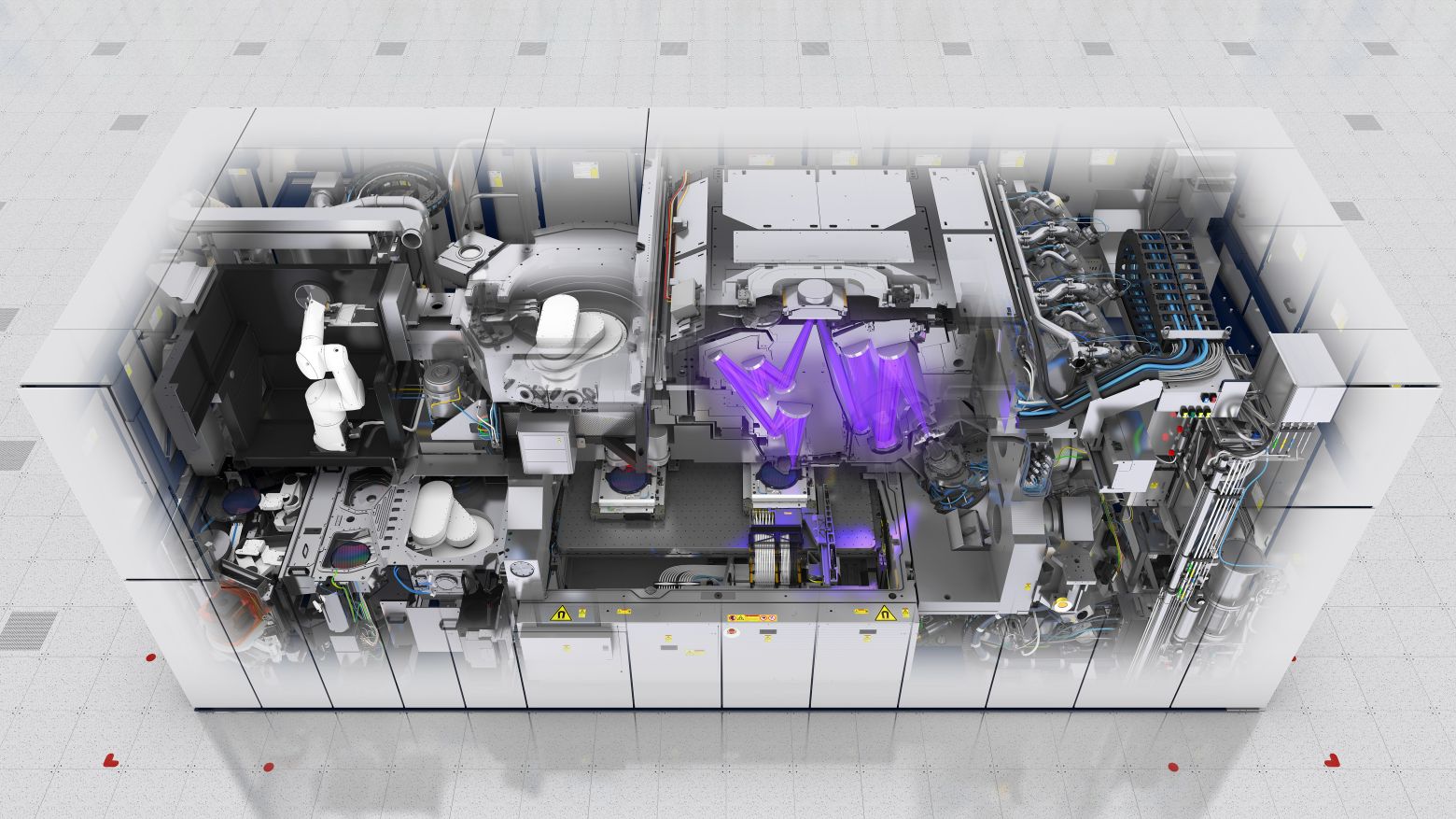
The ASML photolithography machine weighs about 180 tons and costs about $ 170 million
Trying to compete with TSMC (Taiwan) in the production of the latest generation of microcircuits, the Samsung conglomerate (South Korea) went to extreme measures. As it became known to Nikkei Asia, in the fall of 2020, the vice president of Samsung Electronics Lee Jae-yong (de facto is the head of all Samsung) flew to the Netherlands to negotiate with the management of ASML , the world monopoly in the equipment market for the most advanced version of photolithography. in deep ultraviolet (EUV).
Nikkei Asia calls this trip in the midst of the pandemic a desperate move. The Koreans are trying to beg for unique ASML scanners, more than 70% of which are now going to their main competitor - Taiwanese TSMC.
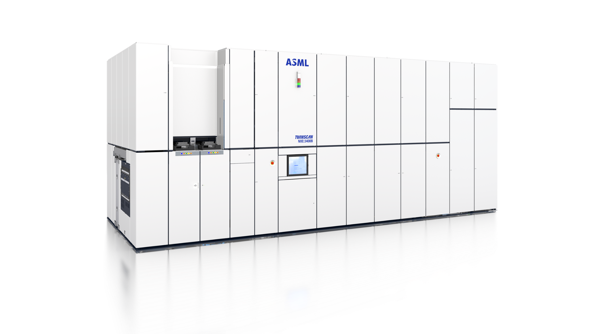
ASML Twinscan NXE: 3400B deep UV photolithography unit supports the etching of 7 and 5 nm elements on an industrial scale (125 or more wafers per hour)
As discussed in the ASML articleThe stepper is the basic equipment that is used in the manufacture of semiconductor integrated circuits. In the process of the stepper's work, the pattern from the mask is repeatedly converted into a pattern on various parts of the semiconductor wafer. The stepper got its name due to the fact that each exposure is made in small rectangular areas (of the order of several square centimeters); to expose the entire plate, it is moved in steps that are multiples of the size of the exposed area (step-and-repeat process). After each movement, an additional check of the correct positioning is carried out.
Modern lithographic installations can use not a step, but a scanning mode of operation; they are called step-and-scan. During exposure, both the plate and the mask move in opposite directions.
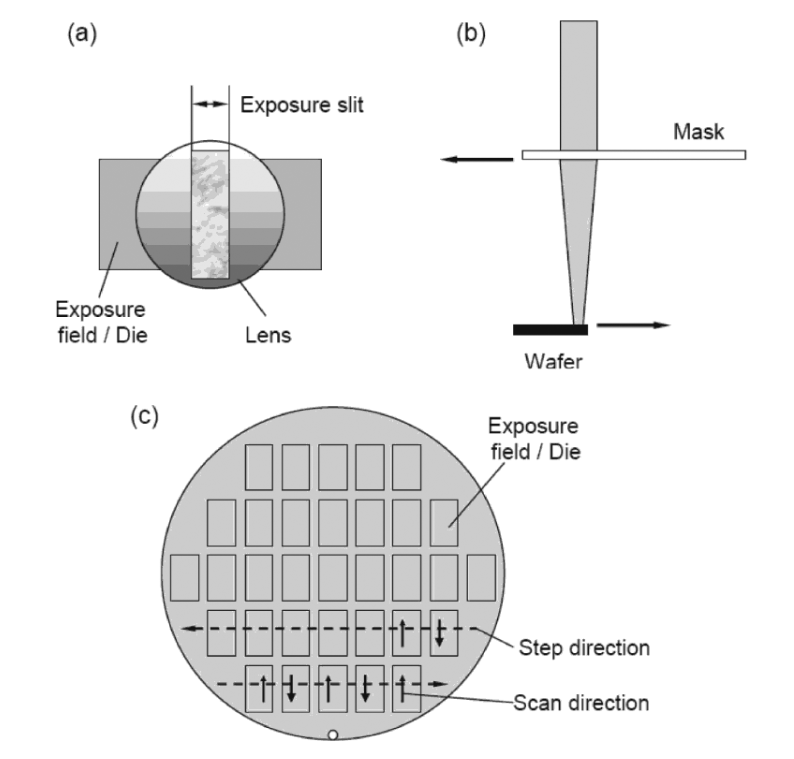
Step-and-scan concept
This equipment is indispensable for the advanced products of the South Korean company. For all the time ASML has manufactured and shipped around the world about 100 of these machines, but more than 70% of them went to Samsung's competitor, Taiwan Semiconductor Manufacturing Co.
Apparently, machines for photolithography in deep ultraviolet according to the 5 nm process technology remain a very scarce commodity, and Samsung is doing its best to acquire them, that is, to increase its quota from ASML.
It should be noted that the stepper / scanner is only one link in the technological chain of dozens of pieces of equipment. Although the main link. The cost of a modern microcircuit factory is approximately $ 10-12 billion, with all the equipment. Moreover, progress is so fast that the plant will become obsolete in a few years. Investments can be recouped only in a very large-scale production.
Nikkei Asia writesthat the trip of Samsung's de facto executive signals a crisis for a company that has ceded TSMC in the field of advanced semiconductors: “Samsung is struggling to mass produce advanced products such as the central processing unit for smartphones and is losing market share in contract manufacturing. The inferiority of advanced products could weaken the competitiveness of other major Samsung products such as RAM and smartphones. ”
For third-party analysts, the technological gap with TSMC is obvious, although Samsung's management refuses to admit it: “Our competitiveness in advanced processes is comparable. We have secured orders from large customers and are closing the gap, ”said Kim Kinam, vice chairman of Samsung Electronics and head of the semiconductor division, when asked about the technology break with TSMC at a shareholders' meeting in March.
However, some vendors say the company has delayed its transition to the state-of-the-art 5nm process. It launched mass production of 5nm a few months after TSMC and the technology gap has widened since then.
Probably, the delay was due to an acute shortage of equipment, which forced the head of Samsung to urgently visit the Netherlands. Apparently, Samsung failed to book as many ASML production facilities as TSMC.
The investment is enormous. In April, TSMC announced plans to set aside $ 100 billion in capital spending over the next three years in response to the global semiconductor shortage.
For comparison, the annual budget of the Russian Federation is about $ 254 billion in revenue.
Samsung plans to invest about $ 40 billion in 2021, but most of it will go to DRAM and other memory chips, and the investment is smaller than TSMC, which specializes in contract manufacturing.
According to Taiwanese research firm TrendForce, TSMC is gaining leadership, increasing its share in contract manufacturing to 56% in Q1. 2021 (+2 p.p. last year, +8 p.p. compared to the year before), while the second-ranked Samsung lost 1 percentage point of the market over the same period.
Large American customers such as Apple and AMD outsource nearly all of their orders to TSMC, making it extremely difficult for another firm to achieve the same production scale.
Growing tensions between the US and China are also playing a role. Taiwan and the US have teamed up against Beijing, while South Korea maintains bilateral diplomacy that risks isolating South Korean companies from semiconductor supply chains, experts fear.
Samsung's declining competitiveness in advanced semiconductors could be reflected in branded smartphones using in-house manufactured CMOS processors and image sensors. Apple is outsourcing all of its processor production to TSMC, so Samsung's technological lag from TSMC may grow into a performance gap between Samsung smartphones and Apple smartphones.