
IBM announced the development of a 2nm process technology.
What was announced:
- 2 nm.
- 50 billion transistors in a nail-sized area. Later they clarified - on an area of 150 sq. Mm - that is, 333 million transistors per square millimeter (
- MTx / mm 2 ).
- The gate pitch of the transistor (Contacted Poly Pitch, CPP) is 44 nm, the gate length is 12 nm.
- (Gate All Around, GAA). – , IBM (horizontal nanosheets, HNS).
- HNS .
- 45% 75% 7 .
- (EUV) HNS 15 70 . , SRAM.
- 5 .
Is this really a 2nm process technology? Today TSMC is the leader in chip production. We plotted the relationship between TSMC process names and transistor density by approximating the curve with a coefficient of determination of 0.99.

From 28nm to 5nm, actual figures are used according to IC Knowledge and TechInsights. 3nm figures are based on TSMC press releases. 2 nm and 1.5 nm is our extrapolation.
Using the graph, you can convert the density of transistors into an equivalent TSMC process technology (TSMC Equivalent Node, or TEN). We get 2.9 nm for 333 MTx / mm 2 . From our point of view, it turns out that this is a 3 nm process technology, not 2 nm.
To compare in more detail the announcement from IBM with previous announcements of 3nm process technology and proposed 2nm process, several assumptions need to be made.
- It is known from the announcement that CPP is 44 nm.
- Suppose production is using the tightest transistor placement technology, Single Diffusion Break (SDB).
- Based on the cutaway photo from the announcement, Buried Power Rails (BPR) is not being used. The BPR is needed to reduce the HNS track size to 5.0 - so let's assume that this value is 6.0 in this process.
- To achieve a density of 333 MTx / mm 2 , the Minimum Metal Pitch would need to be 18 nm - a very aggressive value that would likely require EUV multi-matrix photolithography.
2nm IBM versus existing 3nm process technology
The following table compares IBM designs with our 3nm process estimates from Samsung and TSMC. We know Samsung is working with HNS too, and TSMC has settled on 3nm FinFET. Samsung and TSMC also announced a 3nm increase in transistor density for their process technology, up from 5nm. Therefore, the density of transistors of all three companies is known to us, and we can calculate the TEN for all. IBM's TEN is 2.9; it can be seen that Samsung has 4.7, and TSMC has 3.0. Again, it turns out that 2nm from IBM is more similar to 3nm from TSMC, while Samsung is lagging behind.
Indicative parameters required to achieve the announced densities are highlighted in red, assuming all companies are using SDB technology. The height of the tracks is the smallest in TSMC, since without BPR in FinFET this parameter can reach 5.0, however, in order for the HNS to have the same height, BPR must be used.

2nm IBM versus existing 2nm process technology
In the following table, we estimated the parameter values for the 2 nm process technology from Samsung and TSMC. In our extrapolation, we assume that companies are using BPR (BPR technology is not yet mature, but will likely come on line when they announce a 2nm process in 2023-2024). Let's also assume that companies adopt the NHS forksheet (HNS FS) architecture to achieve a track height of 4.33. CPP and MPP estimates are based on current trends in technology miniaturization.

Power consumption and performance
This year I already made guesses about power consumption and performance of devices from Samsung and TSMC using additional performance data from Intel. The extrapolation is based on company assurances and real-world comparisons between 14nm and 16nm processes.
Since IBM has compared the improvements in power consumption and performance to advanced 7nm manufacturing processes, I can plot their data on the same graphs.
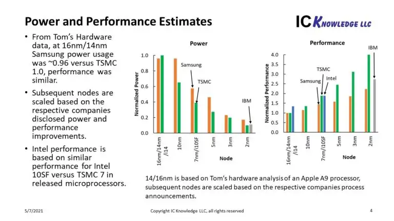
Through the use of HNS, IBM has seen significant power savings, making their 2nm process more efficient than the 3nm process from Samsung and TSMC. Although, in our opinion, when TSMC switches to HNS at 2 nm, their power consumption will not be inferior to that of IBM. In terms of performance, we assume that TSMC's 3nm process will outpace IBM's 2nm process.
Of course, these are all just estimates based on a large number of assumptions.
Conclusion
After analyzing the IBM announcement, we come to the conclusion that their 2 nm process technology is more similar to the 3 nm process technology from TSMC in terms of the density of transistors, while having the best power consumption indicators, but inferior in speed. The statement from IBM is impressive - however, this is just a laboratory sample, clearly surpassing 3 nm from TSMC only in power consumption. At the same time, the first risky batches of 3 nm devices from TSMC will appear this year, and commercial ones next year.
In our opinion, TSMC will maintain the advantage in density, power consumption and speed of devices based on the 2nm process technology when they go into production in 2023-2024.