I want to share my project created in Factorio based on the logic offered by this game. This project was inspired by a great mind who wrote down a step-by-step guide to create almost the same car, but in the real world. I recommend watching it, it will help you understand and recreate this project: 8-bit computer
I bow my head to Ben Iter, who taught me so much through his channel, and I want to devote this little project to him. Great job Ben!
Here is a computer calculating the Fibonacci number, after exceeding the 8-bit limit (number 255), it performs a conditional branch and starts over:
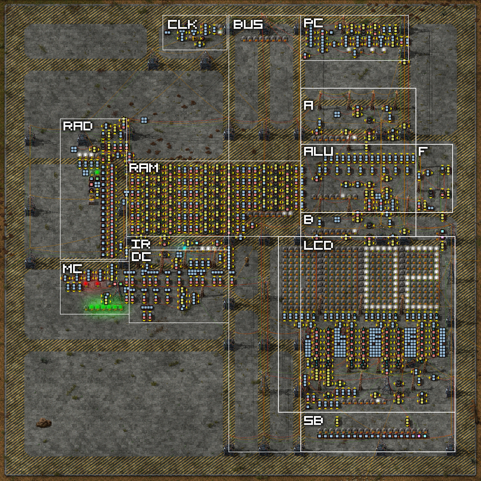
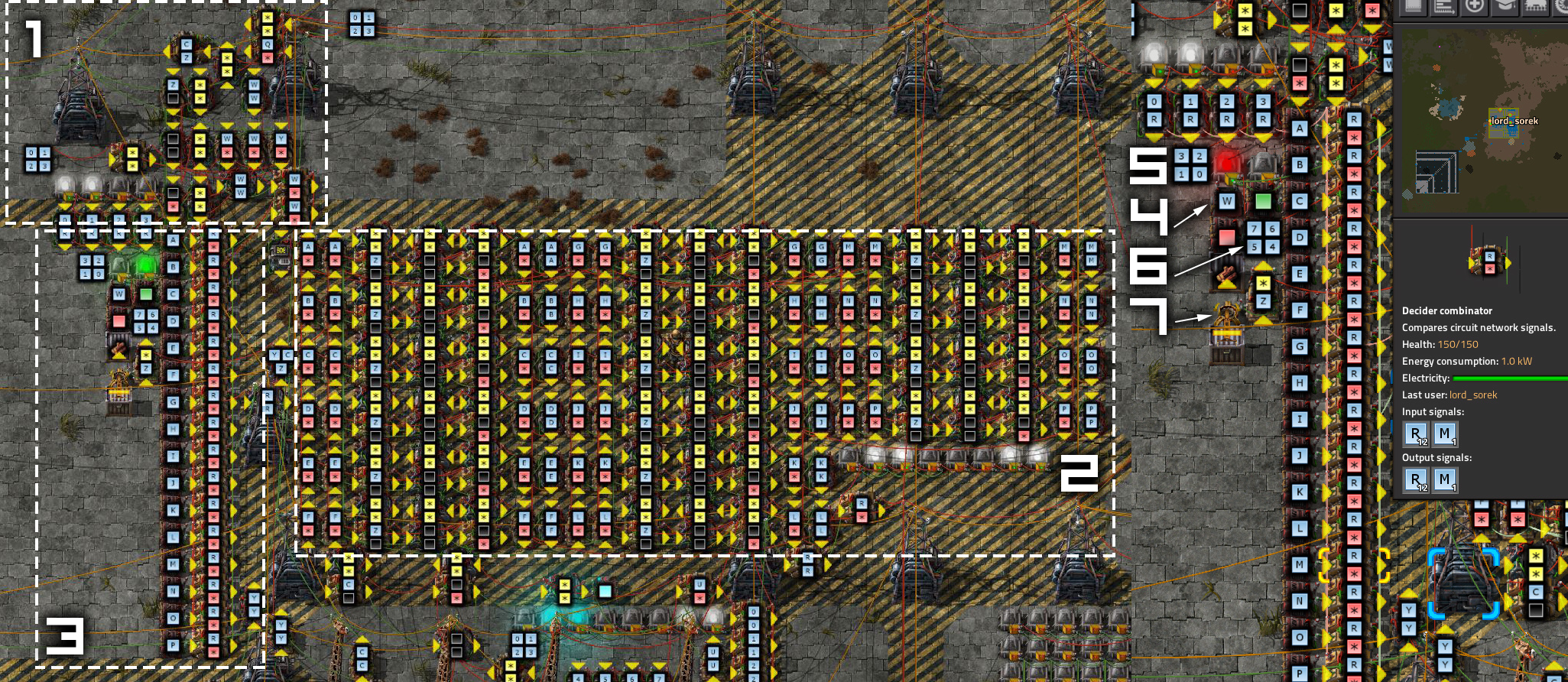
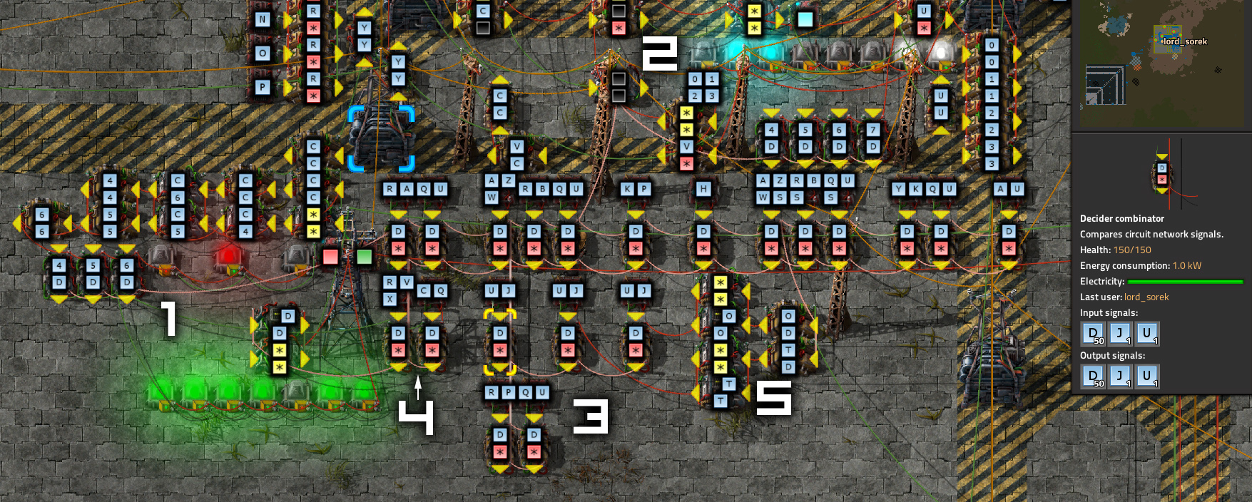
Let's see how this computer works. And fear not - I'm sure that with the basics you can do it too! Let's start with the general layout of the computer. Here I have highlighted the important areas. Below I will explain how I created them.
CLK is a timer that provides machine synchronization. Modern CPUs are capable of operating at 4-5 GHz (4-5,000,000,000 Hz). At the moment my machine can run at 2 Hz due to the limitations of Factorio logic gates - each input must be calculated for each combinator (gate), so if we have 10 in a row, then we need to wait 10 game clock cycles (fps) to start the next cycle of the system. Otherwise, the signals will be confused and the calculation will not be performed.
PC (Program Counter, program counter) - the counter tells which part of the program we are in. Programs are read from 16-byte memory (one byte contains 8 bits). The counter counts up to 16 (4 bits) in binary format (0000, 0001, 0010, 0011, 0100, 0101 ... 1111), so each of these calculations gives us a register address, which we can later retrieve from memory and perform with it actions. It also contains a Jump that resets the counter. We can enter a different value to go to a specific location in our memory / code.
BUS is the main connection point for all computer components. We can transfer data to / from it. To do this, we use control signals that open / close the gates of each component, so that more than two gates are never open (thus the data is not mixed).
ALU is our "calculator" that performs addition and subtraction operations (it can do much more on more complex CPUs!). It instantly receives what is in registers A and B, and then performs logical operations (we select the operation by the instruction decoder). Then this data is output to the bus (bus). ALU also stores flags that can be used in conditional branch functions.
Registers A and B - they can store 8-bit numbers, which are later concatenated in the ALU. Both registers can send and receive data from the bus.
Register address / Decoder (RAD) - reads a 4-bit address from the bus and decodes how much RAM we should read. For example, address 1110 contains the value 0000 0011 (see image).
RAM - Modern PCs typically have approximately 16 GB of memory (16,000,000,000 bytes). We only have 16 bytes ... This leaves us with enough space for 16 instructions or fewer instructions so that we can store data / variables in other parts of memory. Basically, the RAM here is 16 different registers, like the ones we use elsewhere, they are just accessed through a register decoder.
Instruction register (IR) / decoder (DC) - We can put data into the instruction register from the BUS and then decode it to tell how the program should behave. Only 4 bits are used (highlighted in turquoise), which gives us 16 types of commands that can be programmed. Let's say we have an OUT command that prints out what is stored in register A. It is encoded as 1110, so when such a command hits the register, we can decode it and tell the computer how to proceed.
Microcode counter (MC) - Similar to the program counter, but located inside the instruction decoder. Gives us the ability to step through each command.
LCD / Screen is actually a register, but more complicated, since it prints its contents on an LCD screen (Lamp-Combinator-Display, "a display of lanterns and combinators").
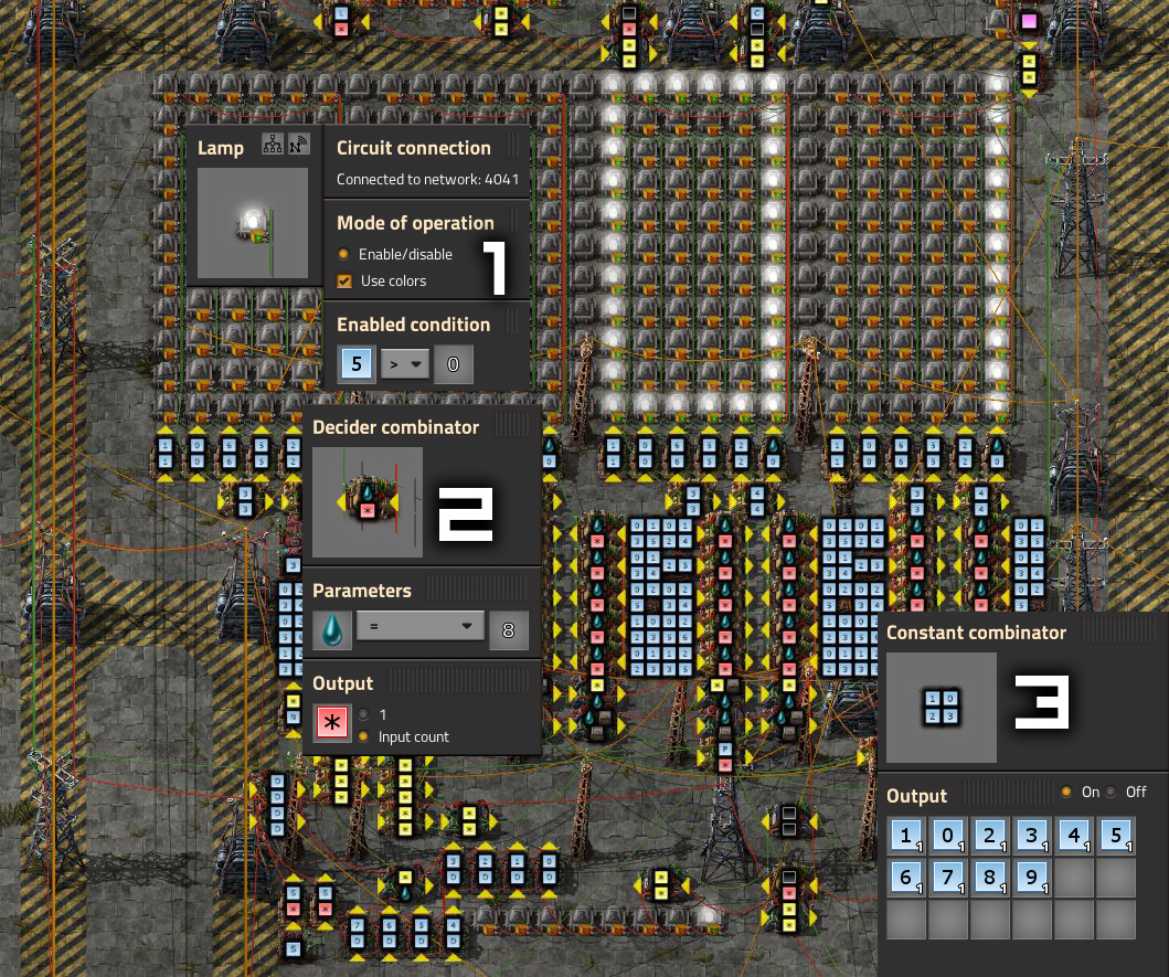
Switch board (SB) - This panel shows us which switch functions we send to control each of the components of the computer. At the moment there are 17 different switches that control different things. For example, if we want to read from BUS to register A, or write to memory / command register, etc. The switches described below can be used to manually control the machine.
Flags (F) - a register for storing flags (carry [T] - when we exceed 8-bit values when adding, zeroing [O] - when the sum / difference is 0). They will help us with the conditional jump commands.
Let me first go into more detail about each component, and at the end we will see how to program a computer, because the process will become clearer. If you are only interested in programming, then skip to the last part of the article.
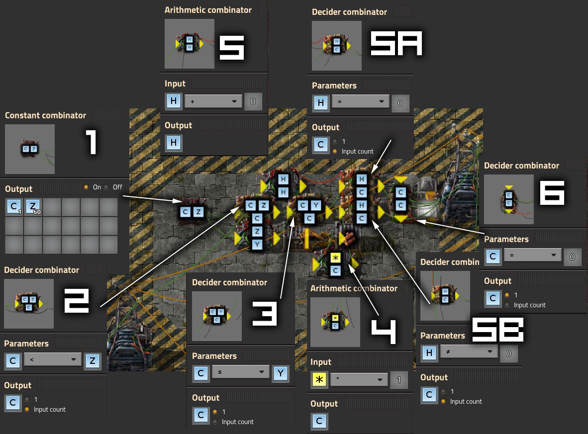
CLK is our timing generator, the most important thing in any computation. I wanted to create an oscillator that has a high [C = 1] and a low [C = 0] signal at the same time.
(1) This is a basic constant combinator that feeds signals to a generator. It jumps to (2) where input and output are merged together. Thanks to this configuration, with each game clock (UPS), the value of [C] is increased by 1. When it reaches [Z], it is reset to 0. That is, Z tells us how many game clock it takes to reset the generator. There is also a simple divisor by 2 below, which keeps the generator high for half the time and low for half the time. When C is less than [Y] (which is half [Z]), the generator is high, otherwise it is low.
The inserter (4) is used as a secondary sync generator in case we need more control over the ticks. If you put something in the first chest, then a beat will happen. If we need 5 bars, we need to place five objects in it.
(5) is the first control signal. [H] is short for the HALT {HLT} command. When it has a low value [H = 0], then the generator operates normally, and if it is high, it goes into manual mode. This is facilitated by the control gates, they (5a) are used for normal operation, and when the signal [H] is not 0, then manual mode is activated and [C] (our CLK) is output.
I also created an inverted signal using the gate (6) - when the output is low, the inverted signal is high. I don't use it in a car, but it's a good idea to remember it for future reference.
Signal [C] travels through the system through the green wire. I wanted to isolate it on a completely separate wire (for example, our BUS is on the red wire) so that it can be easily tracked and not confused with other signals.
Registers - don't be intimidated by them. This is probably the most complex part of the entire system, but it is important to understand how the entire machine works.
Registers contain values. In ordinary life, we would have to create a register for each of the 8 bits and other signals. Fortunately, Factorio allows you to send multiple signals over a single line. Essentially, these are JK triggers.
Briefly about how they work. On each sync pulse, they flush what's inside and keep the incoming value. If there are no incoming values (all zeros), they are cleared in the sync cycle. Of course, we don't want them to be always empty, after all, we need to store values in them. Therefore, we use the control logic, which I will now talk about, and we will deal with the black magic of creating a trigger later.
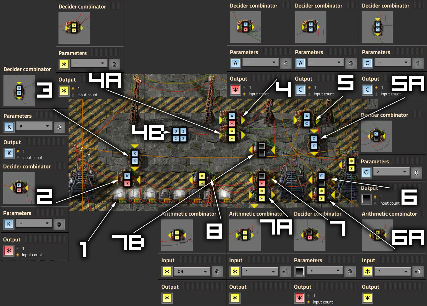
The stored values (1) are displayed with flashlights. When the light is on, it means 1, and off it means 0. As you can see, we are currently storing the value 1110 1001.
To output the value to the bus, we use the gate control logic (2). When the [K] signal is low, this gate outputs whatever is inside the register to the main bus.
Why do we use it when the signal is low and not high? Because logic gates output everything that is supplied to them (red *), and as a result, the bus will have a signal [K], and we do not need this, we only need [7, 6, 5, 4, 3, 2 , 10]. For the same reason, we need to filter out the control signals with the gate (3) so that we receive [K] only when we need it.
The gate (4) is connected to both the bus (red wire) and control signals (green wire). As in the previous case, the register receives an input when the signal [A] is low. To filter out all other signals, we use a logic gate (4a). In fact, it takes all inputs from the bus and unwanted control signals, and then adds them to the combinator (4b), whose inputs are always signals [7, 6, ... 0] = 1. Then if any of the signals is 0, then it outputs each of these signals = 1. It's simple, right? In this case, only those values from the bus that are important to us get into the registers (values 0 will still be 1, they flash for one clock cycle, and then remain disabled throughout the entire high CLK cycle).
In such a situation, when [C] goes high, the shutter (6) outputs the [BLACK] signal, and the shutter (6a) nullifies [C]. But since it takes 1 more UPS to reduce to zero, the gate (6) outputs a signal in such a short time.
This signal is then transferred to the gate (7), which also opens for a short time. The gate (7b) nullifies the [BLACK] signal so that it is not stored in the gate (8), which is used as the custodian of our signal. This is similar to the CLK net, because both the input and output are connected together. If there is no input, then it remains unchanged. If we change the clock once again without entering new data, then the gate (7a) will enter a signal inverted relative to the value stored in the register to clear it.
Now that we know how change recognition and registers work, we know almost everything.
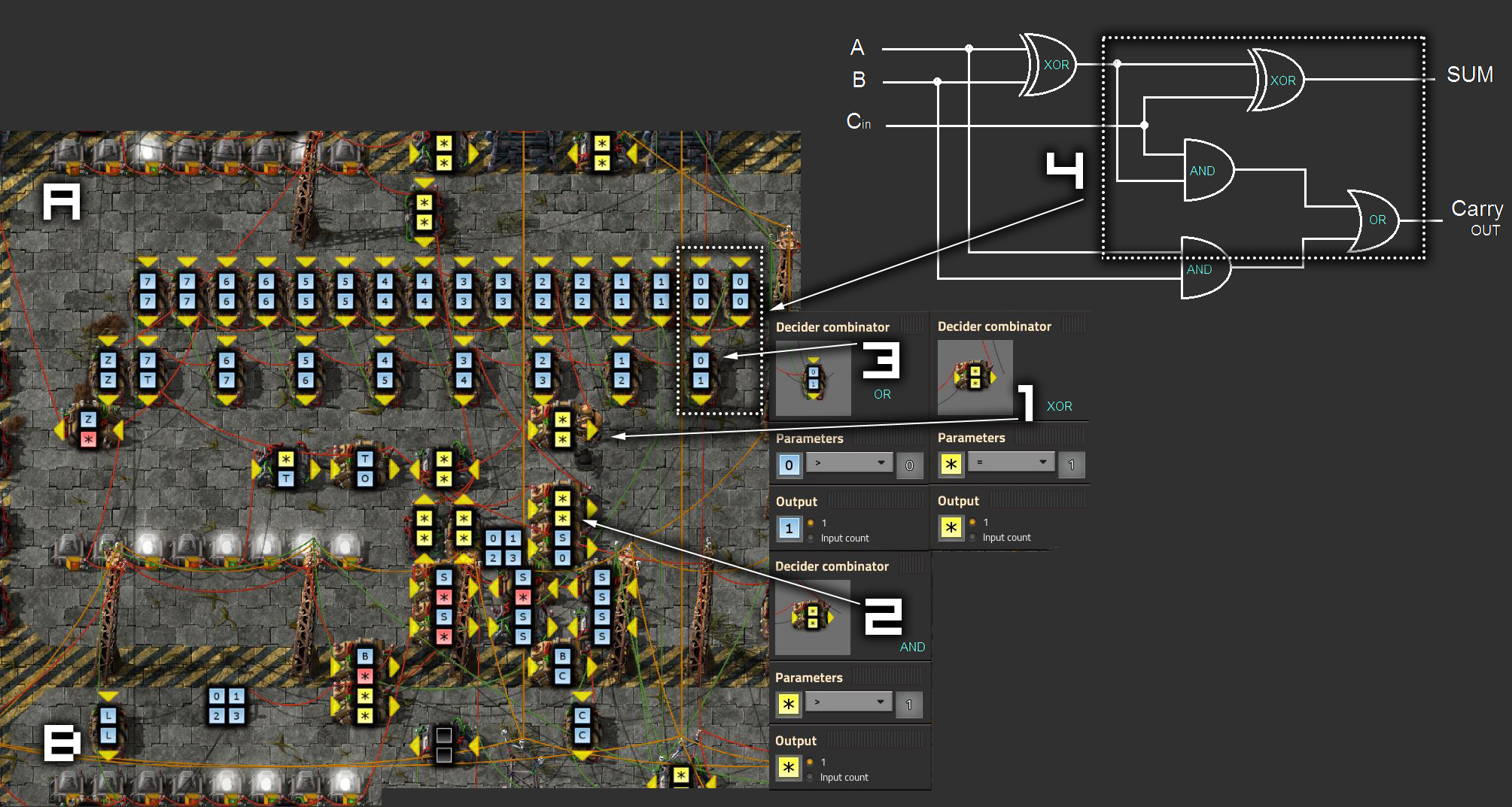
ALU - constantly add / subtract what is in registers (A) and (B). We only control whether to output it to the [Z] bus or change the mode to subtract [S].
How it works? To get the full picture, I recommend watching some of Ben Iter's videos, because the explanation will be three times longer than my article.
I will only explain how to create such an adder in Factorio.
To do this, we need three types of gates: XOR (1), AND (2), and OR (3). Fortunately, they are easy enough to create. Since we can use multiple signals on the same line, our first XOR and AND gate can be simplified to just two, and we don't need to do them for all 8 bits. This allows us to make (4) part of the chain and duplicate it for each bit.
Subtraction is performed with signal [S], which inverts the signals coming from register (B).
ALU also outputs carry (when the sum exceeds 8 bits), zeroing and stores it in the register on the right (F in the image with the main computer).
LCD / Screen - Looks intimidating, but honestly, it was the easiest to make. It only takes time to connect everything correctly.
First, we create a register whose input is controlled by the [P] signal. Then we multiply each bit by its value, converting it to a decimal value to get the same signal with a decimal value (this is kind of cheating in Factorio, but the lack of programmable EEPROMs does not allow us to turn around too much). To convert, we just need to take the first bit [0] and multiply it by * 1, then take the second bit [1] and multiply by * 2, the third [2] by * 4, and so on. In the process, we output to some arbitrary value to determine the resulting number (in this case, it is [a drop of water]).
LCD turns on in 9 steps for numbers (3). We just need to set those lights corresponding to steps (1), and then use the gates (2) to output the value exactly where we need it. You just need to remember to add a separate constant combinator (3) and connect it to only one special gate (2). Then we simply connect all the lights to each other and give them instructions on which step they are in (1).
RAM / Memory Register (RAD) - Here I will explain how RAM works roughly.
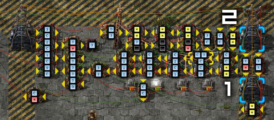
We already know registers that use sync pulses to store values. RAM is just a grid of 16 (in our case) different registers (2). Their inputs are controlled by another register (1) that stores 4 bits [0, 1, 2, 3], which tells us which memory location we are pointing to. This is implemented using an address decoder (3), which works in a similar way to LED / Screen. Each gate receives a value from the constant combinator (in our case 1100 bin = 10 dec) and then outputs the signal name of the corresponding register (in our case [M]) so that the value can be accessed (in our case 00110 0011).
Manual memory programming is also worth mentioning here. This can be done using the [W] signal, enabled / disabled using the constant combinator (4). Another combinator (5) allows us to change the address, and we use another combinator (6) to enter the value. In the end, we just put everything in the chest (7), so that during synchronization, manually transfer the values to RAM, without touching the main CLK of the computer.
Program counter (PC) - its task is to calculate at which program step we are (1). At startup, it has a value of 0000, this address is read from RAM and transferred to the command register for interpretation. After the command completes, we can increment the counter with the signal [X], then it becomes equal to 0001, and on the next iteration this address is taken from memory, and the loop continues.
Of course, sometimes we need to perform unconditional or conditional branching to other parts of the program. We can do this with the signal [J]. If it is low (in our case, low means active), then it is reset, reads from the bus the address to which it should jump, and stores it in register (2). When [J] goes high again, it signals the change detector (located just below 2) to the PC.
The counter itself works similarly to CLK, but instead of constantly counting clock cycles, it counts clock cycles when changes in CLK are detected (in fact, only when X and CLK are active). This can be seen right in the image (1).
The signal can then be applied to the bus using the control signal [C].
Switch board (SB) - This is the right moment to explain each control signal used in the program.
The signals are divided into two colors, green ones go to the left, red ones go to the right. Each signal from constant combinators is actually passed as values [-1]. That is, when the combinators are set to *! = 0, they can output signal 1. Due to this, when the control logic sends signal [1], they are canceled, and we get [0], and in all cases we need just this (you can read in the part where I explain registers).
[H] - stops the clock generator (switches to manual mode), a high signal means that CLK is not switched.
[Q] - the address of the RAM in which the register is located, with a high signal, the RAM address register will save the value from the bus in the next CLK cycle.
[Y] - RAM memory input, when the RAM signal is high, it will save the value from the bus in the next CLK cycle (at the address stored in the address register).
[R] - RAM output, when the RAM signal is high, it outputs the value to the bus in the next CLK cycle (from the address stored in the address register).
[V] - input of the command register, with a high signal, the command register saves the value from the bus in the next CLK cycle.
[U] - output of the command register, when the signal is high, the command register outputs the value to the bus in the next CLK cycle (only the last 4 bits [3, 2, 1, 0]).
[C] - output of the program counter, when the signal is high, the program counter outputs the value to the bus in the next CLK cycle (only the first 4 bits [7, 6, 5, 4]).
[J] - entry of the transition address, when the signal is high, the program counter will set the value from the bus in the next CLK cycle (only the last 4 bits [3, 2, 1, 0]).
[X] - increasing the value of the command counter, when the signal is high, the program counter performs an increment in the next CLK cycle.
[A] - input of register A, with a high signal in register A, the value from the bus is saved in the next CLK clock cycle.
[K] - output of register A, with a high signal from register A, the value is output to the bus in the next CLK clock cycle.
[Z] - ALU pin, when the ALU signal is high, it outputs the value to the bus in the next CLK cycle.
[S] - subtraction (ALU), when the signal is high, the ALU changes its mode from addition to subtraction.
[B] - input of register B, with a high signal in register B, the value from the bus is saved in the next CLK cycle.
[L] - output of register B, with a high signal from register B, the value is output to the bus in the next CLK clock cycle.
[P] - entering the LCD / screen register, when the signal is high, the value from the bus is saved to the LCD / screen register in the next CLK cycle, and this value is displayed.
[W] - input of the flags register, when the signal is high, the flags register saves carry from ALU (when 8 bits are exceeded), zero (when ALU operation = 0000 0000).
[pink signal] - carry flag raised [T]
[turquoise signal] - zero flag raised [O]
Now let's say we need to perform an OUT action: take what is in register A and print it to LCD / screen (register) ... To do this manually, we just need to turn on (by turning off the constant combinator for a certain letter) the [K] signal (output of register A -> bus) and the signal [P] (bus -> register input lcd / screen), then execute the CLK clock.
Command register / decoder / microcode counter - this is where the magic begins. Now that we know how to manually control a computer, this will help us understand. what needs to be done so that he can manage himself.
(1) the microcode counter will count to 8 (the number can be reduced if we do not need that much), that is, we can execute 8 different on / off commands to perform an action in one command.
(2) commands are read into a register from the bus, for this we need to turn on the signals [C] (output of the command counter -> bus) and [Q] (bus -> input memory address), and then read RAM [R] (output RAM -> bus) to the command register [V] (bus -> command register), and also to increment the counter [X].
Since all the above actions need to be done every time, I connected all this (4) directly to the microcode counter so that this happens every time the counter goes through steps 0 and 1.
When there is something in the register, we can use truth tables similar to the ones we created for the RAM address register and output to the LCD / screen.
The [D] values from the command register (it is always greater than 8) and the microcode counter (always equal to or less than 8) can be added, and using the resulting number, we can create logic gates. This is done by gates (3).
The example shows the command 0110 XXXX (48 + X in dec, for which I programmed the JMP command), which is then added to step 2 of the microcode counter, which gives 50.
Another example: command ADD (0010 XXXX - 16 + X in dec); after steps 0 and 1 the microcode will be 2, that is, registers 18-24 can be used for another part of the code (in this case, we only need 18-20, since ADD is a 3-step process).
(5) Carry flags are processed by simple logic gates, input is disabled on them only if no carry [T] or zero [O] is applied to the logic gates.
Below is my complete list of implemented commands (you can change them or add your own!):
0 NOP - 0000 XXXX - does nothing.
1 LDA X - 0001 XXXX - loads the value from the X RAM address into register A.
2 ADD X - 0010 XXXX - loads the value from X RAM address into register B, and then outputs the addition and places it in register A.
3 ADD X - 0011 XXXX - loads the value from X RAM address into register B, and then outputs the subtraction and puts it in register A.
4 STA X - 0100 XXXX - loads the value from register A and stores it in RAM at address
X.5 LDI X - 0101 XXXX - quickly loads the value from the command register (only 4-bit value) into register A .
6 JMP X - 0110 XXXX - unconditional (always occurs), the transition to the value X (PC assigns the value of X).
7 JC X - 0111 XXXX - when carry value [T] is true, jumps to value X (assigns PC to X).
8 JO X - 1000 XXXX - when the transfer of zero [O] is true, then it goes to the value X (assigns the PC value to X).
9 OUR X - 1001 XXXX - displays the value from the X RAM address.
...
...
...
14 OUT - 1110 XXXX - Performs display from register A (X does nothing).
15 HLT - 1111 XXXX - stops the sync generator (X does nothing).
Let's write a simple program and see how it works!
0 LDA 3 - load the value into register A from the memory address 3
1 OUT - display the value from register A.
2 HLT - stop CLK, that is, the whole machine.
3 42 - stored value
That is, in fact, this program outputs the value stored at address 3 RAM (0011 in binary).
Let's convert it to binary:
0 Address: 0000, value: 0001 0011
1 Address: 0001, value: 1110 0000
2 Address: 0010, value: 1111 0000
3 Address: 0011, value: 0010 1010
That is, to write a program, we need to write to memory (W on the memory panel; see the part with the RAM image), starting at address 0000, and enter the value 0001 0011 inside (0001 means the LDA command, where 0011 is X, that is, address 3 in memory) ...
Then we do the same for the other teams.
Don't forget to turn [W] green again and save halt to the counter.
You can also reset the PC by jumping with J (there is no need to change the CLK beat).