This article continues a series of articles on the history of processors and platforms for them, started with stories about the Pentium Pro , Pentium ( part 1 and part 2 ) and Pentium II . Intel's "golden age" continues, the sky still looks cloudless, but clouds are already gathering over the horizon. Ready to travel back in time again?
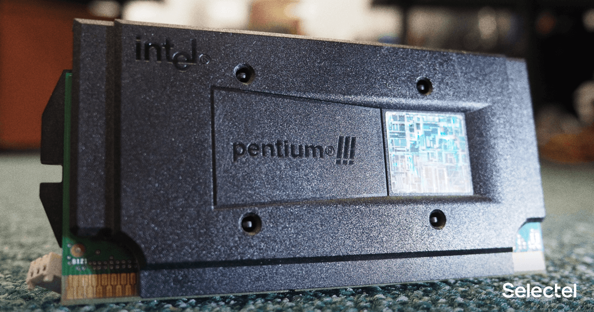
Our starting point is February 26, 1999. On this day, Intel presented its new family of processors: Intel Pentium III on the Katmai core. From a marketing point of view - another breakthrough, conquering new heights of productivity and efficiency. But from the technical point of view, the new processors practically did not differ from the previous, not at all old Pentium IIs - the technical process (250 nm) was preserved, the frequencies slightly increased.
Of the deeper changes - an improved first-level cache controller and an updated FPU - do not at all pull on an additional "one" in the name, right? And here's why these executive changes were needed, according to marketers, just pulled for an increase - a set of SSE (Streaming SIMD Instructions) extensions, Intel's answer to colleagues from AMD with their 3DNow!
Two from the casket and one wife
Indeed, the Pentium II "Deschutes" and the Pentium III "Katmai" are remarkably similar to each other. Let's tell you a secret - even the processor board in the cartridge is identical. Only the BGA chip soldered in the center of the board has become a little larger - 128 mm 2 instead of 113 mm 2 . Frequencies - Deschutes ended at 450 MHz, Katmai kicked off with 450 and 500 MHz versions. The same technical process and a similar complexity of the cores gave the same power requirements - 2.0 V (for later older versions - 2.05 V). And, the crown trick of Intel - the new processor did not receive new chipsets when it was released.
As mentioned in the previous article, the result was an amazing situation - processors belonging to different generations in marketing did not use just one chipset (as is the case with 440FX and Pentium Pro / Socket 8 and Pentium II / Slot1) or even one more connector (like the late Pentium and Pentium MMX), but also did not require any hardware changes in the motherboards! Only software update BIOS with newer microcodes.
The Pentium III was easily plugged into early Intel 440BX-based motherboards such as the Asus P2B, and many out-of-the-box system manufacturers released Katmai-based computers where replacing the processor was the only change. There were even lines where Pentium II and Pentium III coexisted within the same model! At the same time, the frequencies of the latter have already reached 550 and even 600 MHz!
However, this story did not last long. First, Katmai appeared with the designation 533B and 600B, their difference from their predecessors was the support for the bus with a frequency of 133 MHz. This is where the first troubles await Intel, but the events of interest to us began to happen a little earlier.
The early Pentium IIIs in the Digital Vintage collection are represented by the ServerGhost Rotoscope P6 / 2 gaming station Asus P3B-F, Intel 440BX. Pentium III 550 MHz, 512 40 IDE . 3Dfx Voodoo 3 3000 AGP 16 — , — , . — Creative SB Live! 5.1. . Windows 98 SE , API Glide.

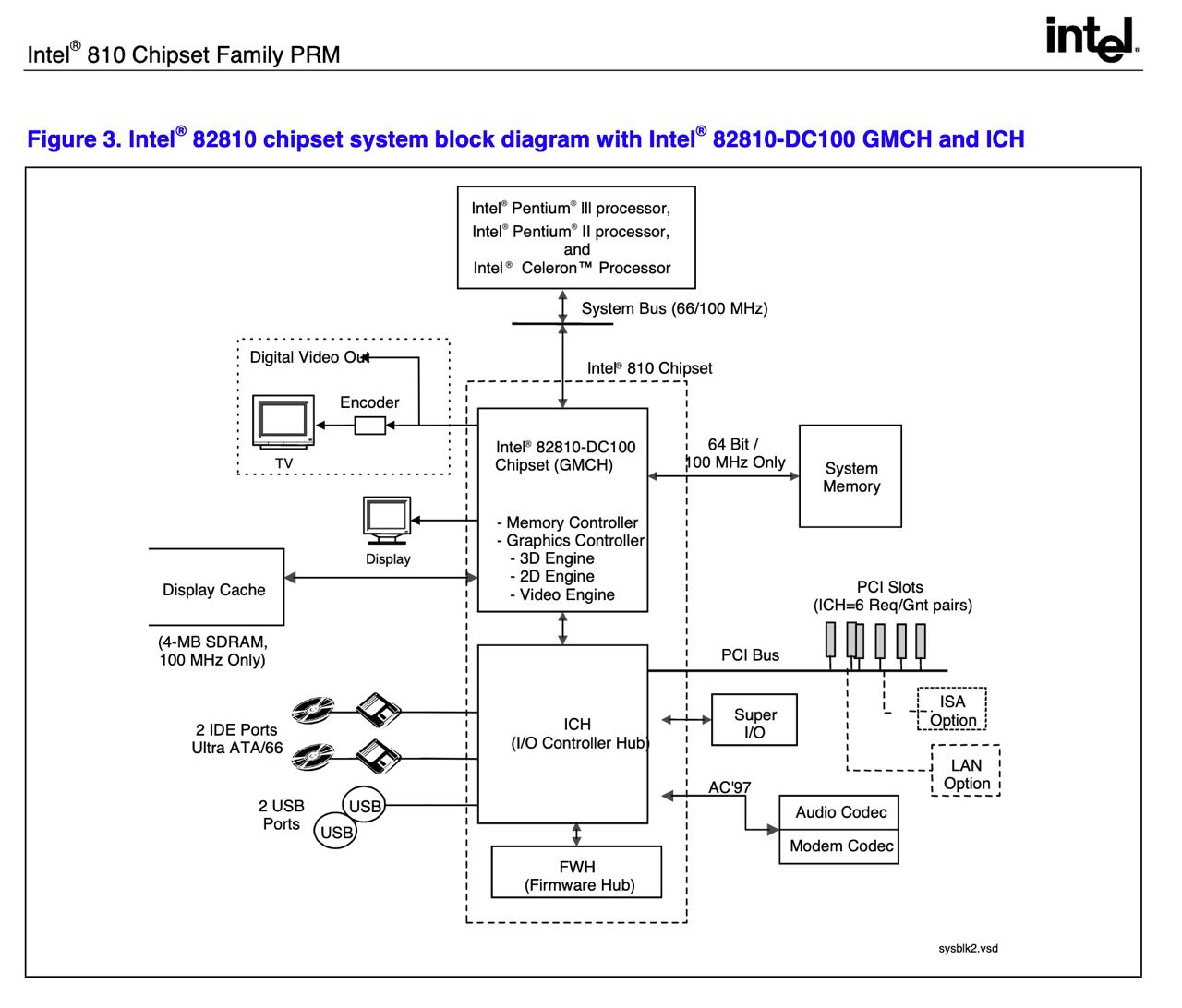
In early 1999, Intel released a highly controversial but truly innovative product - the Intel 810 "Whitney" chipset. It so happened that most users are familiar with it from inexpensive and not very productive computers of the early 2000s, when the chipset was already an openly weak solution. But at the time of release ...
Top graphics solutions at that time were nVidia Riva TNT2, ATi Rage 128, Matrox G400 and 3dfx Voodoo 3 - the last truly successful product of the famous company. They carried on board from 8 to 16 MB of video memory (32 MB versions will appear later) and used a 128-bit bus to work with it.
Even then, the cost of such video cards was comparable to the cost of a good motherboard. And here Intel releases an integrated (the first in its history) solution with an integrated sound controller (it was necessary to add only a codec and an analog part) and a fairly serious 3D accelerator.
Its performance was at the level of the previous generation cards (there were no budget solutions as such, the former leaders simply fell into this segment after the release of new ones) - approximately between Riva 128 and Riva TNT, depending on the implementation. The functionality is quite adequate at that time, including support for DirectX 6.0. The GPU itself (however, there was no such term yet in those days) was based on the rather successful Intel 740 solution, released a year earlier. Its functionality was improved (i740 only supported DX5.0) and the core frequency - from 66 to 100 MHz.
The original used a 64-bit memory bus with a frequency of 100 MHz, which gave a bandwidth of up to 800 MB / s when using 4 or 8 MB of local video memory. The AGP 2x interface allowed accessing the system memory at speeds up to 533 MB / s, slightly slower than local memory, which allowed not to waste time on transferring data to video memory before processing - the card was optimized for this type of operation.
In the integrated video core Intel 810 (it received the designation i752, discrete video cards with this core were also released in extremely small volumes) this idea was brought to the absolute! At system startup, the video core used 1 MB of system memory for the frame buffer; when loading drivers, this value could dynamically (hence the Intel DVMT technology - Dynamic Video Memory Technology, which is used to this day) increase to 4 MB, allowing you to switch to higher resolutions.
Another 2 MB were reserved when launching a 3D application for the command cache and 4 for the Z-buffer. Total - up to 12 MB. All the work with these textures was carried out using the system RAM! In the Intel 810-DC100 version, video memory chips were installed on the motherboard, or rather "display cache" in Intel terms - they were used for the Z-buffer. The size of such a "cache" was fixed - 4 MB, and access to it did not take up the bandwidth of the main RAM.
Working with memory resembles a simplified implementation of UMA (Unified Memory Architecture - a unified memory architecture, as opposed to SMA - a shared memory architecture in most other integrated chipsets). For the sake of speed of memory access (and at the same time simplification, of course), the chipset lacks AGP support. The video core itself uses a kind of "Direct AGP" operating at a speed equal to the speed of access to the memory system - the same 800 MB / sec as the local video memory of its predecessor.
The memory controller itself was significantly optimized - even using the memory shared with the video card, the version with the display cache was practically not inferior in performance to the famous 440BX, in terms of the speed of working with SDRAM it remained unsurpassed. True, the leaders of the graphics industry by that time switched to a 128-bit bus and a faster 200 MHz memory, which increased the bandwidth fourfold - despite a good start, it was not destined to keep up with them in the future.
Doesn't sound very impressive? Now let's imagine that in comparison with the current situation, along with the motherboard, the user received a "free" video card of the GeForce GTX1660 Super or RTX2060 level (for options with and without display cache) at the top-end RTX3090. Intel 810 allowed playing modern games with medium graphics settings in 640x480 resolution, which was quite popular at that time. True, this technological advancement negatively affected the creation of drivers for alternative operating systems, especially open source - until the mid-2000s they were considered extremely unstable, but now Intel's video is the most stable option for Linux users.
But it was not only the level of integration and integrated video that this chipset was unusual. Intel previously tested new technologies on entry-level chipsets (for example, i430VX was the first to receive SDRAM support), and this time - Intel 810 became the first chipset with the so-called "hub architecture".
Basically, this meant the abandonment of PCI as a bus for connecting the north and south bridges, which were now called hubs - GMCH / MCH (Graphics / Memory Controller Hub), in which, as before, the key components of the system and ICH were located (I / O Controller Hub) - I / O bus hub. Even for a flash drive with a BIOS code, they came up with a new name - FWH (FirmWare Hub). The PCI bus for connecting bridges was replaced by a proprietary bus with twice the bandwidth compared to the previous version. Accordingly, the PCI controller left for the south bridge, taking the place of ISA - it was completely abandoned.
The chipset was initially aimed at the market of inexpensive computers and was seen as a pair of Celeron in Socket 370. The main options were:
- Intel 810 — «» ICH /66.
- Intel 810L — ICH0, ATA/33 4 PCI
- Intel 810-DC100 — ICH.
The chipset supported processors with 66 and 100 MHz buses and SDRAM memory with a frequency of 100 MHz, while the memory controller became asynchronous - it became possible to clock the memory regardless of the processor bus. Most of the first generation motherboards on it were released in MicroATX format and supported only Celeron processors (Socket 370) on the Mendocino core. However, there were also motherboards, including full-sized ones, with Slot1 for Pentium II / III and slot Celerons.
Soon a version of the chipset with support for 133 MHz of the processor bus appeared - Intel 810E / 810E-DC100, while the memory controller tightly integrated with the video core remained working at the same 100 MHz.
Epic refusal
Intel planned to expand the use of the 133 MHz bus, the upcoming Coppermine were to become the main beneficiaries of its implementation. For processors with a fast bus, a new chipset was also required, a successor to 440BX - this role was assigned to the Intel 820 "Camino" - with support for AGP 4x and a new type of memory - the infamous RDRAM created by Rambus (also known as RIMM - Rambus Inline Memory Module ).

RDRAM itself on paper was very good - a narrow 16-bit bus at an extremely high frequency, from 600 to 800 MHz, was supposed to simplify the layout of the boards and raise the speed of working with memory even higher. Intel still relied on the use of system memory for storing textures during video processing, and therefore required a higher bandwidth than the processor bus required (1200-1600 MB / sec versus 1066 MB / sec).
In the process of fine-tuning the chipset and the memory itself, it turned out that due to the high frequencies, the bus is extremely susceptible to various pickups and interference, and the memory chips also get pretty hot during operation. To reduce the influence of interference, it was necessary to install special C-RIMM modules in empty slots. And all the same, instead of the planned 3 modules on one channel (and the Intel 820 was developed as a single-channel chipset), no more than two could work simultaneously at 800 MHz - most of the boards ended up with 2 memory slots.
RIMMs were released in sizes up to 256 MB (later 512 MB modules were not supported by the chipset). As a result, with a maximum supported amount of up to 1 GB of memory, the actual was 512 MB at 800 MHz or 768 MB at 600 MHz and in the "if you're lucky" format. It was especially funny to see dual-processor motherboards with only a couple of memory slots and support for 512 MB versus 1 GB of the predecessor!
But the real problem was not the amount of memory, but its cost - the prices for RIMM were multiple, and sometimes by an order of magnitude higher than the prices for the usual and slightly slower SDRAM. Already in the later stages of development, Intel had to create a classic "crutch" - the MTH chip, the Memory Translation Hub. Thanks to it, it became possible to create cards with SDRAM support and even hybrid ones - with RIMM and DIMM slots (without the possibility of their simultaneous use).
Finally, in November 1999, the chipset saw the light of day. It would seem that all his problems have been solved. But no - the "crutch" turned out to be weak, errors were found in its work, which could no longer be corrected programmatically. All boards released with its use have been recalled - finding one of them is not an easy task these days. And motherboards based on Intel 820 with RIMM did not gain any noticeable popularity either. Their main application is mid-range workstations with one or two processors.
There is no copper here!
Almost at the same time, in October, another very important announcement took place - new Pentium IIIs based on the Coppermine core were released. They were already manufactured using the 180 nm process technology, which made it possible to reduce the core area and integrate the second-level cache on the die. He received half the size - 256 KB, but worked at the core frequency and had a wider bus for data exchange - 256 bits (Katmai and Deschutes worked with a 64-bit bus).
This cache acceleration perfectly compensated for the reduced cache size and allowed the new processors to perform on par with or even outperform their predecessors. Coppermine was released in variants from 500 to 733 MHz and used a bus of 100 or 133 MHz. In addition to the models in the Slot1 construct, there were also released models in the "Seleron" Socket 370 construct.
This was a real Pentium III - finally, a critical mass of improvements deserving a model number increase! Although, it should be noted, the "large" on-chip cache has already been tested on the mobile version of the Pentium II "Dixon" (but the width of the bus connecting the core with the cache was 64 bits, not 256), who was the first to try on the new technical process. Another interesting fact - at that time the transition to the use of copper inter-chip connections instead of aluminum was discussed and many thought that the name Coppermine (from English - copper mine) was chosen for a reason. But no - only chips released according to the next generation process technology - 130 nm - received copper interconnect.
VIA seizes the initiative
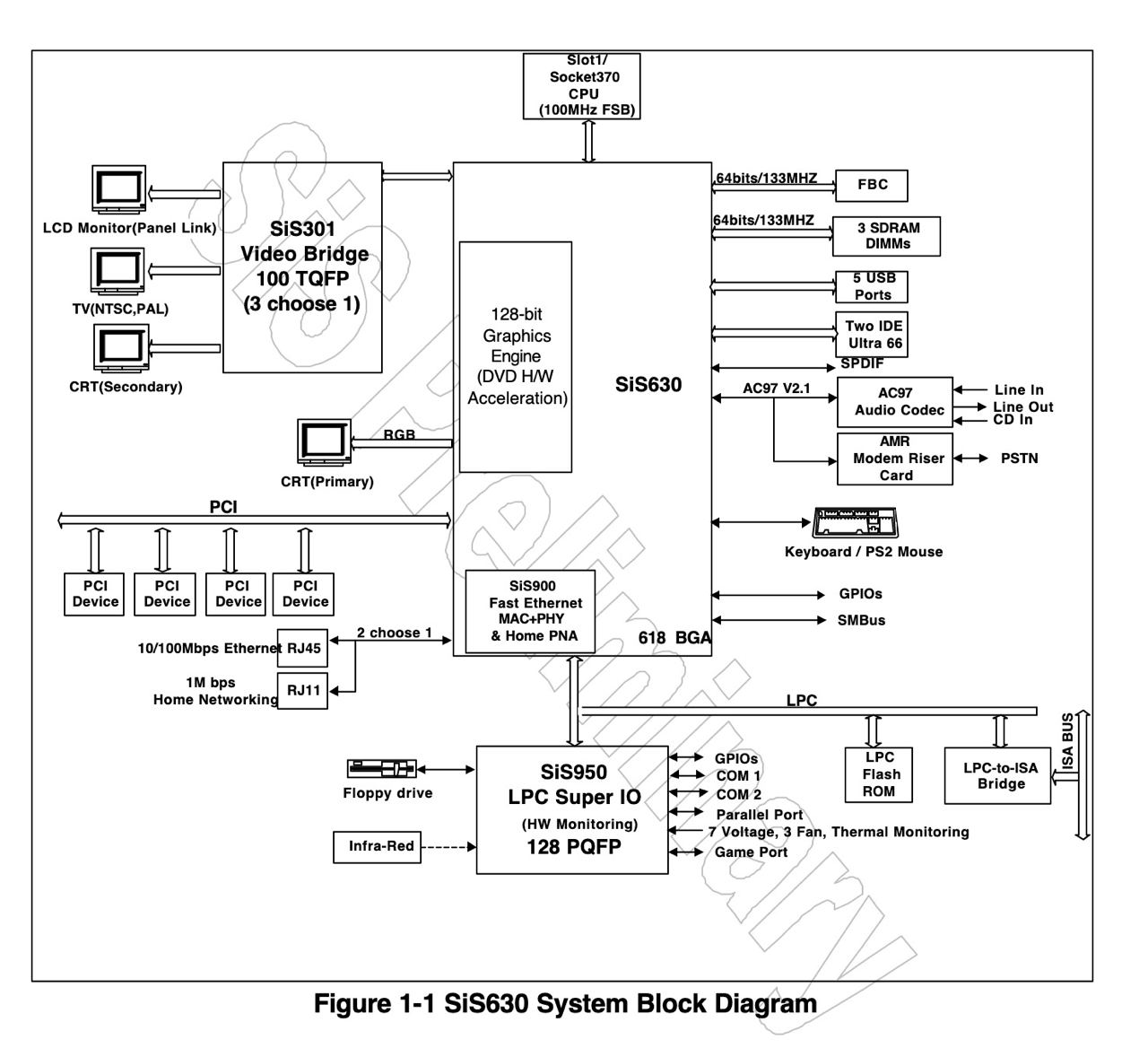
According to the original plan, Intel 820 was supposed to occupy not only the upper, but also the middle segment. But because of the problems that arose, the Pentium III B / EB (as the models with 133 MHz bus were designated) did not receive a decent mid-level chipset. On the one hand, this fact undoubtedly made life difficult for Intel, and on the other hand, it gave rise to a variety of motherboards based on third-party chipsets, unprecedented since Pentium times. SiS and ALi performed relatively modestly, and the most notable of them was, perhaps, the SiS 630, an ultra-budget integrated chipset, compared to which even the Intel 810 seemed to be a very powerful solution.
By 2000, ALi had an interesting trump card up its sleeve - Aladdin TNT2, which had a full-fledged TNT2 M64 on board (even with the ability to install dedicated memory) and which could become the king of integrated graphics and beat buyers from discrete video cards of the middle segment, but the company played this card I could not. Then VIA turned around in full - this time was the period of its heyday, its chipsets during the "reign" of Coppermine not only compared, but also surpassed Intel in terms of market share.

The first were Apollo Pro Plus (VIA 693) and Apollo Pro 133 (VIA 693A) - still budgetary, relatively slow chipsets. Both supported AGP 2x and ATA / 66, the first worked only with 66 and 100 MHz bus and supported 1 GB of memory, the second received support for the 133 MHz bus for the processor and memory and could already work with 1.5 GB of RAM. These chipsets proved to be very reliable and stable, but the speed of their work was depressing - the memory controller let down. The controller itself, inherited from earlier models, was very flexible and could demonstrate good performance, but only a few motherboard manufacturers gave access to these settings - by default, the boards were configured for greater compatibility.

breakthrough was Apollo Pro 133A (VIA 694X / DP) - most of the compatibility problems have already been resolved, support for AGP 4x and the ability to work in a dual-processor mode appeared. Up to 2 GB of RAM was already supported, although most boards were equipped with three slots and could only work with 1.5 GB, respectively. Asus P3V4X (single-processor Slot1 board) and Asus CUV4X-DLS (dual-processor Socket 370 with 4 DIMMs and onboard network and SCSI controllers) are deservedly considered the best motherboards in this series.
Seeing the success of Intel's integrated solutions and looking back at its own successful MVP4 solution for the Super 7 platform, VIA has released a whole galaxy of embedded video solutions. By that time, VIA had acquired a whole galaxy of chip developers - S3, Trident, IDT / Centaur, Cyrix. This even made it possible to provide 3D cores - a faster S3 Savage solution (VIA PM133) was available for budget home computers, and an ultra-cheap Trident Blade3D solution (VIA PL133 with AGP and PLE133 without AGP) for less demanding office solutions.
Despite solving the problems with the memory controller, the chipset drivers remained the weak point. Moreover, the problem was not so much in the drivers themselves, but in a very buggy installer, with an interface that allowed for discrepancies. Especially many problems were caused by AGP drivers, without which many interface functions, for example, GART, did not work, and the port itself worked much slower than required, and with the installed drivers it was possible to get an unstable working system if you did not follow the sequence of actions strictly recommended by enthusiasts.
All these chipsets used VIA 596B / 686A / 686B south bridges connected via the PCI bus. They supported a standard set of functions - ATA / 66, USB1.1, ISA. Bridges of the 686 series received an integrated audio controller of the AC'97 standard and the functionality of the SuperIO controller (monitoring, serial and parallel ports, etc.), version B was distinguished by support for the ATA / 100 interface. At the same time, it is believed that the 596 bridges were more stable in operation, and for ATA / 100 the PCI bus bandwidth was a limiting factor, because it was used in one way or another by other peripheral devices, and already two ATA / 66 channels could use its full bandwidth ...

In 2000, one of the most productive variants appeared - VIA Apollo Pro 266 - the first and only chipset for Pentium III with support for DDR memory (up to 4 GB!). This chipset was already ideologically close to the DDR chipsets for the AMD K7 platform, it used the proprietary V-Link bus for connecting bridges, which had a performance similar to the Intel inter-hub bus.
The old men go to battle again
And so, in the Intel camp, the flanks were adequately covered, but the center was unforgivably weakened. While the preparation of a decision was underway, which could radically improve the situation, the battle was taken by a veteran volunteer. It turned out to be the well-known Intel 440BX chipset. Intel did not release the long-awaited version with official support for 133 MHz bus and, of course, did not authorize the release of motherboards with factory overclocking. And nevertheless, it was they who became the saving link, allowing to wait for the release of the new platform.

That the 440BX overclocks well has been known for a long time - many second-generation motherboards announced in early-mid 1999 supported bus overclocking much higher than 133 MHz, provided the power required for Coppermine, and, most importantly, some of them already had the ability to install a PCI bus divider 1: 4, which ensured its normal operation. There was no possibility to add a divider for correct AGP operation, the closest to the standard value was 89 MHz (133 / 1.5) instead of 66 MHz.
On the one hand, not all video cards were capable of operating at an increased interface frequency, but the most popular and productive solutions from nVidia easily took these frequencies. On the other hand, due to the increased bus frequency, the lack of support for the AGP 4x mode was partially leveled out - the gain in bandwidth relative to the standard mode was about 30%, which added a few percent to the overall performance in games and 3D applications.
In 2000, the third generation of motherboards based on 440BX appeared - as a rule, they were equipped with Socket 370, guaranteed to operate at 133 MHz (the guarantee, of course, was solely on the conscience of the manufacturer). Often these boards were equipped with additional ATA / 66 or even ATA / 100 controllers, sometimes even with RAID support - from HighPoint or Promise. Often, high-quality sound solutions were installed, up to the integration of the basic models of SoundBlaster chips from Creative (CT5880), built-in network cards appeared. For fans of external expansion devices, basic models of motherboards were produced, for example, one of the best motherboards of its time, Chaintech 6BJM, the successor to the famous 6BTM, had neither sound nor an additional IDE controller on board.
Intel asymmetric response
Meanwhile, in the dark forges Intel was preparing a crushing response to VIA - the new Solano chipset, which was designated Intel 815 when it was released. The chipset turned out to be fast, reliable, but extremely controversial. Let's look at the characteristics and decide what went wrong:
- Supports processors with Pentium III / Celeron with 66/100/133 MHz bus, only single-processor configurations are officially supported.
- Supports up to 512 MB SDRAM PC133 RAM, up to 4 banks, non-ECC unbuffered memory only, asynchronous memory mode.
- Seriously redesigned memory controller (relative to i810) - the frequency can vary from 66 to 133 MHz, it can correspond to the bus frequency or differ from it by 33 MHz up or down.
- AGP 4x bus support (except 815G / GE).
- Optional - integrated video based on the seriously modified Intel 752/754 video core, up to 8 MB of dynamically allocated DVMT video memory (Intel 815 / 815E / 815G / 815GE with video, Intel 815P / EP - without).
- Supports ATA / 66 or ATA / 100 (Intel 815E / EP with ICH2 Southbridge).
- Supports 4 USB 1.1 ports.
- Built-in AC'97 audio controller.
Most users decided that this is a slightly updated i810 and the main difference is the AGP slot. For the majority, in fact, the capabilities of the chipset were enough - everything you need is on board, there is AGP for a video card, there is enough memory (back then, mid-range PCs were often equipped with 128 MB of RAM, 256 MB was the lot of advanced machines).

Advanced users noticed that the new chipset did not inherit the beloved 440BX, it could only replace the 440ZX! Of course, few people needed ECC support, and even more so register memory, but the ability to install 1 GB of RAM using up to 8 banks was a reasonable necessity for those who planned to use a computer for a long time and use it not only for basic needs. Many enthusiasts are accustomed to reasonable prices for dual-processor motherboards based on mid-level chipsets (recall that 440LX / BX were just mid-level chipsets, the top one was 440GX).
In reality, one small but very proud company - Acorp, in 2001 (when Pentium 4 was already on sale with might and main!) Released a series of dual-processor motherboards based on i815. These were models 6A815ED (built-in video and sound, IDE RAID controller), 6A815EPD (built-in sound and IDE RAID controller) and the most common model - 6A815EPD1 (no additional controllers at all). A computer with the latter was at one time at the author of the article as a home machine.
Also mentioned is a server / industrial version of this board for installation in 1U rack cases, but they are not on sale nowadays, perhaps only demo samples were released. The Acorp 6A815ED is the only dual-processor board with integrated video in the chipset and uses the SMA architecture with dedicated video memory from the system memory (the second exception is the non-IBM PC-compatible SGI Visual Workstation 320/550 systems mentioned in the last article).
But back to the chipset. Despite the similarity of characteristics to the i810, it differs from it almost as much as it differed from the i440 family! Most importantly, Intel abandoned UMA and returned to the classic SMA architecture, but with dynamically allocated video memory. This allowed us to use the standard AGP implementation, but the performance of the embedded video dropped somewhat, despite the improvements in functionality and improvements. The possibility of installing the "display cache" was retained - now it was just video memory, it was executed in the AIMM format - a memory model for installation in an AGP slot.
Changes were also made to the memory controller, as a result of which it became somewhat slower than the i810, the difference was even more significant compared to the 440BX. Among the advantages of the memory controller is support for memory chips with a density of 256 Mbit, which reduced the complexity of choosing modules by 256 Mbytes and ... made it possible to set the maximum volume using only one module. Most i815-based motherboards had 3 memory slots; among compact models, there were often motherboards with two slots.

But there were also "four- slot " motherboards, for example, the Abit SA6 - from which the rapid development of the "full-size" direction in the "Digital Vintage" collection began. Another interesting board was released for the off-the-shelf HP Vectra VL systems in MicroATX format. This board used a full version of Intel 815 with integrated video, an AC'97 codec and a 3Com network controller are integrated on the board, and there are two memory slots. A special feature is an optional sub-board installed in an ATX case and connected to the main flexible cable. Together they form a full-size ATX system. The subcard contains an ISA bridge made by ITE and a pair of ISA slots for special cards, classic sound cards and modems.
The overwhelming majority of motherboards based on i815 series chipsets carried Socket 370. Only one motherboard with Slot1 is known - Abit SH6 with 4 memory slots, integrated video and sound, and an optional additional IDE controller.
An interesting fact - some sources claim that the i815 version without integrated video was not a rejection of the integrated version, but had a different die with a smaller area.
Coppermine is represented by two systems. ServerGhost Rotoscope P6 / 3 classic entry-level workstation based on Abit SA6 board and low-cost 2-processor ServerGhost Catalina P6 / 3L TE systembased on the same Acorp 6A815EPD1. Both are equipped with 733 MHz Pentium III processors, 512 MB of RAM and a 40 GB hard drive (IDE). The video subsystems differ - a single-processor machine is equipped with a Matrox Millennium G450 DualHead with 32 MB of video memory, a dual-processor machine is equipped with an nVidia GeForce 2MX with the same memory capacity. The systems work under Windows Millennium Edition and Windows 2000 Professional, respectively.


To be continued ...
At this point, we will probably interrupt. The history of the Pentium III turned out to be too eventful and it is impossible to fit them into one article without making it too heavy. See you!
In the second part you will find:
- Chasing gigahertz
- Deadborn Timna
- Life after death
- Travel to parallel worlds