The crystal oscillator is an important electronic component that provides very accurate clock generation for little money. Due to the piezoelectric effect, its electrical properties change during vibration. Because it is possible to make a crystal that vibrates at a specific frequency, crystal oscillators are very useful for a variety of applications. They appeared in the 1920s and first provided accurate waveform generation for radio stations. In 1970, a revolution of wristwatches took place , when they began to use high-precision quartz oscillators. Computers from the 1940s ENIAC to this day use crystal oscillators to generate the clock frequency.
Modern PCs still use crystal oscillators, but more sophisticated technologies are used to obtain multi-GHz clock speeds. The PC uses a crystal with a frequency much lower than the operating frequency, and multiplies it using a phase-locked loop. Computers often use a 14,318 crystal because that frequency was used in older televisions and were inexpensive and widespread.
In order for the crystal to vibrate, its circuitry requires additional components. In the 1970s, modular crystal oscillators gained popularity - these compact and easy-to-use micro-assemblies combined the crystal itself, the IC and discrete components. I wondered how one of these modules worked, so I opened one of them and reverse-engineered its chip. In this post I will explain how it works and describe the tiny CMOS circuit that drives it. It turned out that there is more interesting going on inside the module than you might expect.
Generator module
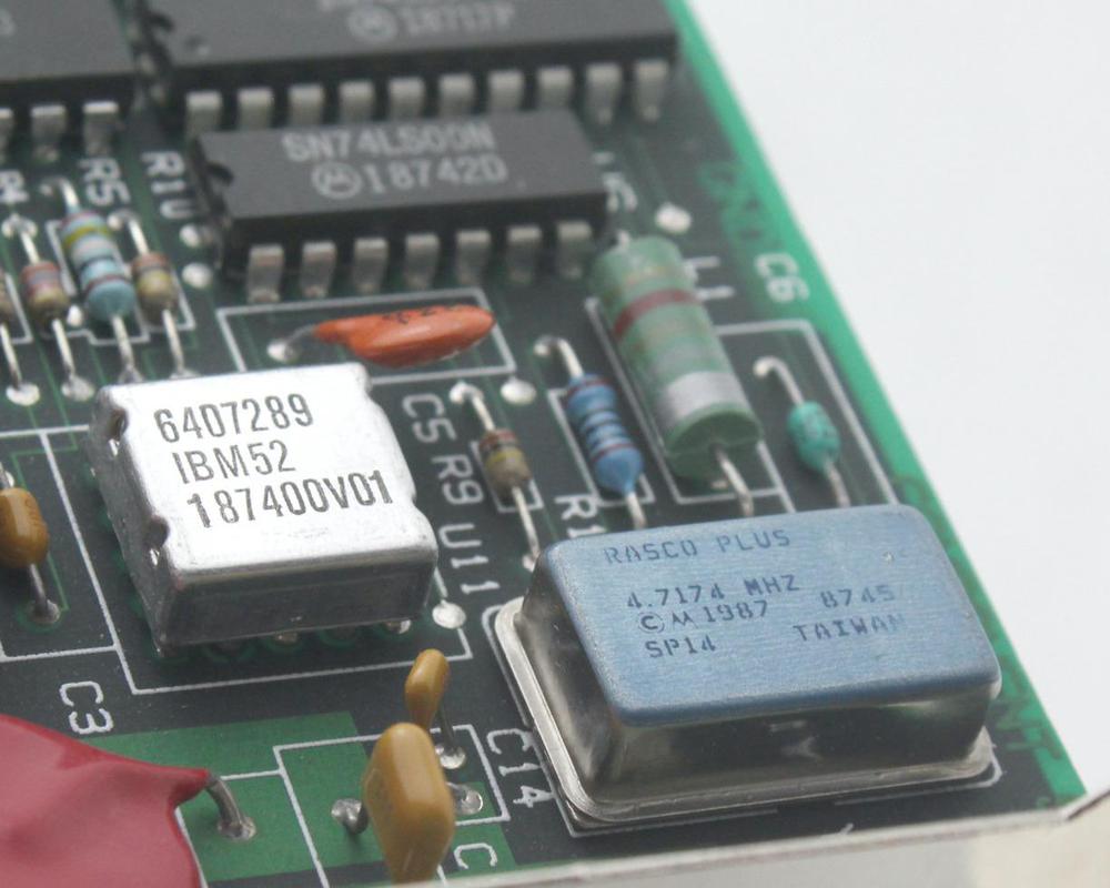
I studied a module from a card for an IBM PC. The module is housed in a rectangular metal case with 4 contacts, which protects the electronics from electrical noise (this is the Rasco Plus in the rectangular case on the right in the photo, not the square IC from IBM). The module generates a signal at 4.7174 MHz, which follows from the inscription on its case.
Why does the card use a crystal with such an unusual frequency - 4.7174 MHz? In the 1970s, the IBM 3270 was a very popular CRT terminal. The terminals were connected by coaxial cable and used the Interface Display System Standard protocol operating at a clock frequency of 2.3587 MHz. In the late 1980s, IBM produced interface cards for connecting an IBM PC to the 3270 network. My crystal is just one of these cards (type 56X4927), and the crystal frequency is 4.7174 MHz - exactly twice the 2.3587 MHz.

The crystal oscillator module is on the bottom right. Body inscription: Rasco Plus. 4.7174 MHZ, Motorola 1987. The square module on the left is an IC from IBM.
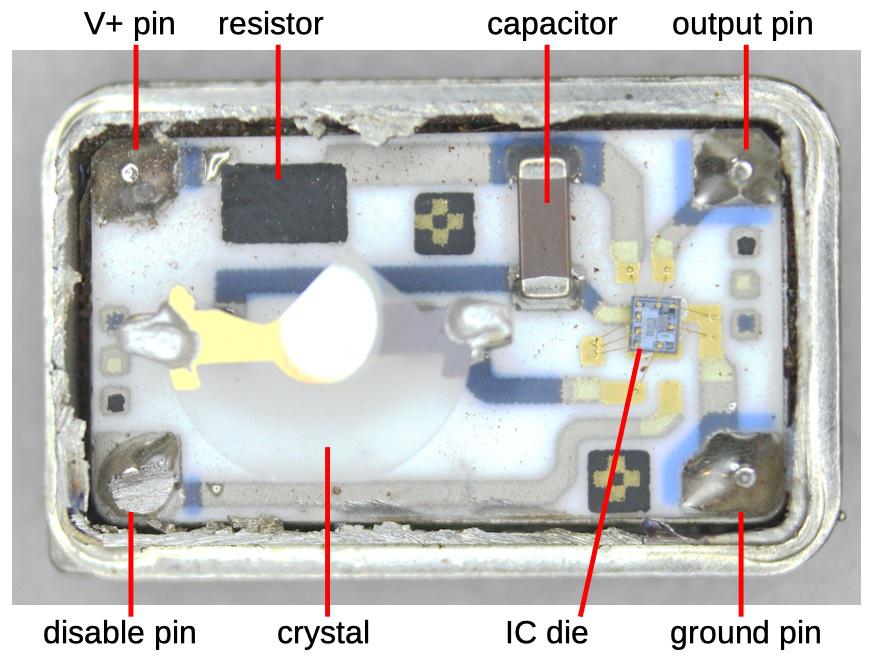
I opened the case of the module to look at its hybrid circuit. I expected to see a quartz crystal there that resembles a gem in a box, but I found that the quartz oscillators use a very thin quartz disc. I damaged it when I opened it, so it is missing a piece at the top right. It can be seen on the left side of the photo - metal electrodes fit to it from both sides. Those, in turn, are connected to small pins on which the crystal is raised above the surface of the case so that it can vibrate freely.
– , . . 3 10 , , , .
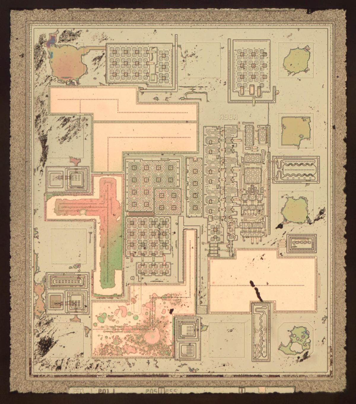
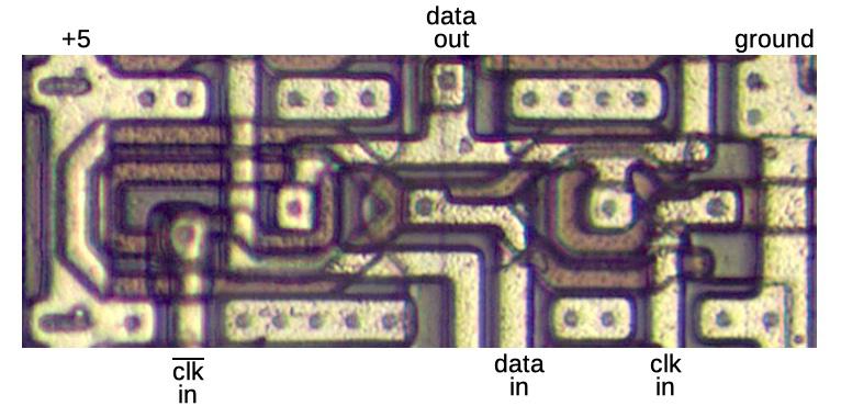
The photo below shows a tiny IC crystal under a microscope. Contact pads and main functional blocks are marked. The green-brown areas are the silicon forming the IC. A yellowish metallic layer connects the components to the IC. Under the metal is a reddish layer of polysilicon, where transistors are formed - but it is almost completely covered by the metal layer. Along the edges of the chip is a weld wire connected to pads connecting the chip to the rest of the module. Two sites (select and disable) are not connected. The chip was produced by Motorola in 1986. I could not find information on the article SC380003.

IC crystal with markings of the main blocks. "FF" stands for triggers. "Sel" - pads [select pads]. "Cap" - pads connected to internal capacitors...
IS has two tasks. First, its analog components cause the crystal to vibrate. Second, its digital components divide the frequency by 1, 2, 4, or 8, and provide a high current clock signal (the divider is set by two select pins on the IC).
The crystal oscillator is implemented according to the scheme below, which is called the " Colpitz oscillator ". It is more complex than a conventional crystal oscillator circuit. The bottom line is that the crystal and two capacitors oscillate at a given frequency. However, the oscillations would quickly decay if it were not for the supporting feedback from the supporting transistor.
A typical crystal oscillator uses a simple circuit called a Pierce oscillator, in which a feedback loop is formed from a crystal and an inverter. The two grounded capacitors in the middle make it very similar to the classic Colpitz generator.

I'm not sure why the crystal oscillator I have disassembled uses a more complex circuit that requires a clever voltage bias.
In 1918, Edwin Colpitz, chief researcher at Western Electric, invented a crystal oscillator with an inductor and a capacitor. Today this circuit is known as the Colpitz generator. The idea is that the inductor and the capacitor form a "resonant reservoir" that oscillates at a frequency dependent on the characteristics of the components. You can imagine that the electricity in this reservoir kind of splashes back and forth between the inductor and the capacitors. The vibrations themselves would quickly decay, so an amplifier is used to feed them. In the original Kolpitz generator, the amplifier was a vacuum tube. Later, the circuits switched to transistors, but this amplifier can be operational or of a different type. In other circuits, the end is grounded so that there is feedback in the middle. Then the capacitors do not invert anything,therefore, a non-inverting amplifier is used.

Simplified diagram of the Colpitz generator with basic components.
The key feature of the Colpitz generator is the two capacitors that form the voltage divider. Since they are grounded in the middle, they will have opposite voltages at both ends: when one rises, the other falls. An amplifier takes a signal from one end, amplifies it, and feeds it to the other. The amplifier inverts the signal, and the capacitors give a second inversion so that the feedback amplifies the original signal (providing a 360 ° phase shift).
In 1923, George Washington Pierce, professor of physics at Harvard, replaced the inductor in the Colpitz generator with a crystal. Thanks to this, the generator became more accurate, and it began to be widely used in radio transmitters and other devices. Pierce patented his invention and made decent money from companies like RCA and AT&T. Availability of patents has led to years of litigation, which has come down as a result of the Supreme Court.
For several decades, the Pierce generator was called the Colpitz generator with a crystal. The Pierce generator often lacked characteristic capacitors, instead of which the parasitic capacitance of the vacuum tube was used. Terminology gradually changed , and the two different types of crystal oscillators began to be called the Colpitz oscillator (with capacitors) and the Pierce oscillator (without them).
Another change in terminology occurred due to the fact that the Colpitz oscillator, Pierce oscillator and the Clapp oscillator were topologically identical crystal oscillators, differing only in which part of the circuit was considered to be ground (collector, emitter or base, respectively). All these generators can be called Colpitz generators, only with a common collector, a common emitter or a common base.
I made this excursion into history in order to show that in various sources these generators are called differently, Colpitz or Pierce generators, and in a contradictory way. The generator that I studied can be called a Colpitz generator with a common drain (by analogy with a common collector). It can also be called a Colpitz generator based on the location of the ground. But historically it can be called a Pierce generator since it uses a crystal. It is also called a single-pin crystal oscillator because only one pin of the crystal is connected to the external circuit (the other is grounded).

Simplified generator circuit
Increasing the voltage on the crystal turns on the transistor, the current goes to the capacitors, increasing the voltage across them (and on the crystal). Decreasing the voltage on the crystal turns off the transistor, the current drain (circle with an arrow) draws current from the capacitors, decreasing the voltage on the crystal. Thus, the feedback from the transistor amplifies the oscillations of the crystal, maintaining them.
The bias voltage and current circuits are an important part of this circuit. The bias voltage sets the gate of the transistor somewhere in the middle between the on and off state, so the voltage fluctuations on the crystal turn it on and off. The bias current is halfway between the on and off currents of the transistor, so the current coming in and out of the capacitors is balanced (I'm simplifying when talking about on and off states - in reality, the signal will be sinusoidal).
Bias and current circuits are moderately complex analog circuits, consisting of a bunch of transistors and a few resistors. I will not describe them in detail, I will only say that they use feedback loops to generate the desired fixed voltage and current values.
A significant part of the IC is occupied by five capacitors. In the diagram, one is on the top, three run in parallel to form the bottom capacitor in the diagram, and one stabilizes the bias voltage circuit. The photo of the crystal below shows one of the capacitors after dissolving the upper metal layer. The red and green areas are polysilicon forming the top plate of the capacitor along with the metal layer. The pinkish area under the polysilicon is probably silicon nitride, which forms a dielectric layer. Silicon with additives, which is not visible in the photo, forms the bottom plate of the capacitor.
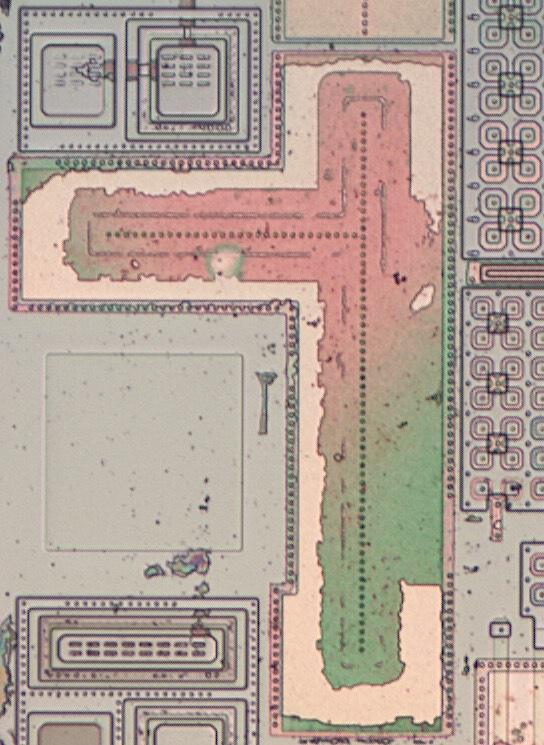
Chip capacitor. The large pale square on the left is the pad for connecting the wire to the IC. The complex structures on the left are the clamping diodes of the contacts. The clover-like structures on the right are transistors.
Interestingly, the capacitors on the chip are not connected together. They are connected to three wires connected to each other. Perhaps this gives the circuit flexibility - the capacitance of the circuit can be changed by removing the conductor leading to the capacitor.
Digital circuit
On the right side of the chip is a digital circuit for dividing the output frequency of the crystal by 1, 2, 4, or 8. Thanks to this, the same crystal can output four frequencies. The divider is made up of three flip-flops connected in series. Each one divides the incoming pulse in half. The 4-to-1 multiplexer selects between the original pulse rate or the output from one of the flip-flops. The selection is carried out using the conductors coming up to the two selection pads on the right side of the crystal. The resulting frequency is fixed at the production stage. Four NAND gates are used together with inverters to decode the pins and generate four control signals for the multiplexer and flip-flops.
Implementation of CMOS logic
Kip is built on CMOS (complementary metal oxide semiconductor) logic. It uses two types of transistors working together, N-MOS and P-MOS. The diagram below shows the structure of an N-MOS transistor. The transistor can be thought of as a source-drain switch that controls the valve. The source and drain (green) consist of sections of silicon with additives that change its semiconducting properties - from N + silicon. The valve is made of a special silicon, polysilicon, separated from the silicon substrate by a very thin insulating oxide layer. The N-MOS transistor turns on when the valve is pulled up.
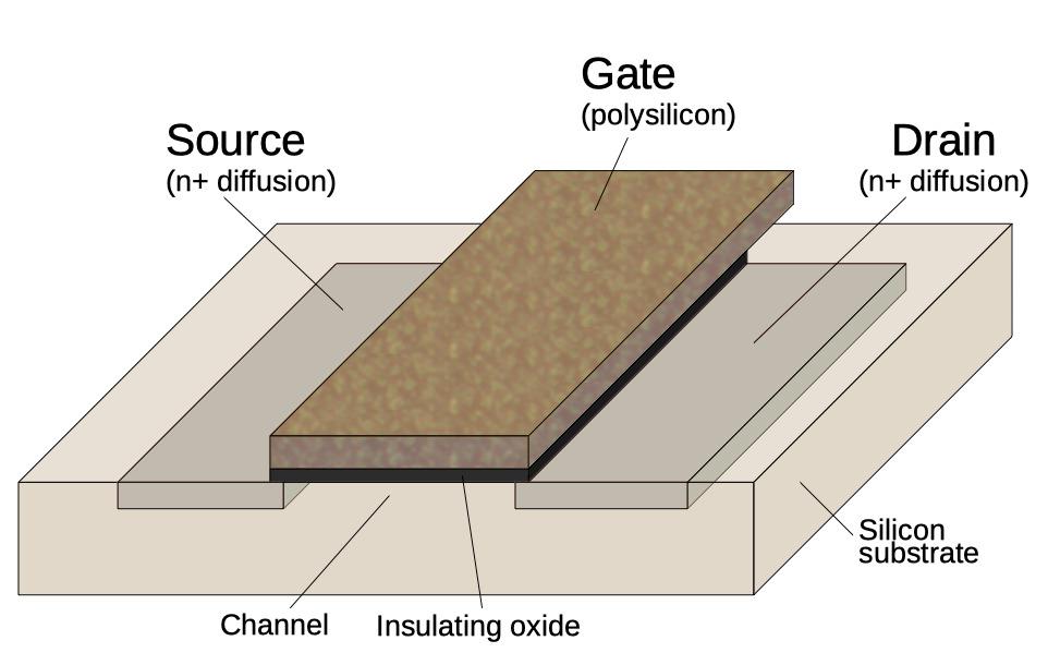
N-MOS transistor structure. The structure of the P-MOS transistor is similar, but the N- and P-type silicon sections are swapped.
The structure of a P-MOS transistor is the opposite of an N-MOS: the source and drain are composed of P + silicon embedded in N silicon. It also works in the opposite way to the N-MOS transistor: it turns on when the valve is pulled down. Typically, P-MOSFETs pull the drain up and N-MOSFETs pull the drain down. In CMOS transistors work by complementing each other, pulling the output up or down as needed.
The diagram below shows how the NAND gate is implemented in CMOS. If 0 is applied to the input, the corresponding P-MOS transistor (top) turns on and pulls the output up. If 1 is applied to both inputs, the N-MOS transistor (bottom) turns on and pulls the output down. Thus, the circuit implements the NAND function.

The diagram below shows how the NAND gate looks on the die. Unlike the pictures in textbooks, real transistors have a complex, sinuous shape. There is a P-MOS transistor on the left side and an N-MOS transistor on the right. The reddish lines above the silicon are the polysilicon forming the valves. Most of the silicon in the substrate is conductive due to the additives, and looks slightly darker than non-conductive silicon without additives at the left and right edges, as well as in the center. For this photo, the metal layer was etched away. The yellow lines represent where the metal conductors used to be. The circles are the bonds of the metal layer with the lower layers, silicon or polysilicon.

How a NAND gate looks like on a chip
The transistor in the photo can be compared to the NAND gate circuit. Take a look at the polysilicon shaped gates of a transistor and what they share. From the +5 section, there is a path to the output through the long P-MOSFET on the left. The second path goes through a small P-MOS transistor in the center - this shows that the transistors are connected in parallel. Each valve controls one of the inputs. The left track from ground to output should go through both concentric N-MOS transistors - they are wired in series.
This IC also uses many ring-gate transistors. This unusual arrangement of elements allows multiple parallel transistors to be placed in high density. The photo below shows 16 transistors with ring valves. The copper-colored clover-like patterns are the drain of the transistors, and the source is outside. The metal layer (here it is removed) unites, respectively, all sources, valves and drains. Parallel transistors work like one big one. Parallel transistors are used to supply high currents to the output. In a bias circuit, different numbers of transistors (6, 16, or 40) are connected together to obtain the desired current ratio.

Transfer valve
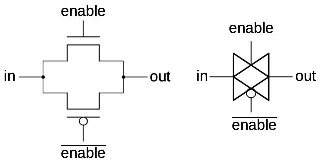
Another key circuit in the chip is the transfer gate. It works like a switch through which the signal either passes or not. The diagram below shows how a transfer gate is made from two transistors, an N-MOS transistor and a P-MOS transistor. If a large voltage is applied to the enable line, both transistors turn on, and the input signal goes to the output. If the voltage is low, they turn off, blocking the signal. On the right is the conventional designation of the transfer valve in the diagrams.
Multiplexer
The multiplexer is used to select one of four clock signals. The diagram below shows how the multiplexer is implemented using transfer gates. The multiplexer accepts four signals as input: A, B, C and D. One of the inputs is selected by activating the corresponding selection line and its complement. This input is connected via a transfer valve to the output, and the other inputs are blocked. Although the multiplexer can be built on standard logic gates, its implementation on transfer gates is more efficient.
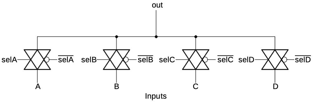
4-to-1 multiplexer based on transfer valves
The diagram below shows the transistors that make up the multiplexer. A pair of transistors is connected to inputs B and C. I think this is done because a pair of transistors has half the resistance. Since inputs B and C are for high frequency signals, a pair of transistors can reduce latency and distortion.

The photo below shows how the multiplexer is physically implemented on a chip. The polysilicon valves are best seen. The metal layer has been removed. The metal conductors ran vertically, connecting the corresponding segments of the transistors. The sources and drains of adjacent transistors are combined into single sections located between the valves. The top box contains N-MOS transistors and the bottom box contains P-MOS transistors. Since P-MOSFETs are less efficient, the bottom rectangle should be larger.

Trigger
There are three flip-flops on the chip that divide the clock frequency. The crystal oscillator uses switchable triggers that toggle between 0 and 1 each time an incoming pulse is received. Since two incoming pulses give one outgoing one (0 → 1 → 0), the trigger divides the frequency in half.
The flip-flop consists of transfer gates, inverters and a NAND gate - see diagram below. When the input clock signal is 1, the output passes through the inverter and the first transfer gate to point A. When the input signal switches to 0, the first transfer valve opens and the previous value remains at point A. Meanwhile, the second transfer gate closes, so the signal passes through the second inverter and the transfer gate to point B. The NAND gate inverts it again, causing the output to be reversed. The second cycle of the incoming clock repeats this process, bringing the output back to its original value. As a result, two cycles of input signals give one cycle of output, so the flip-flop divides the frequency by 2.

Each trigger has an enable input. If a trigger is not needed for the selected output, it is disabled. For example, if the division by 2 mode is selected, only the first flip-flop is used and the other two are disabled. I guess this is done to reduce power consumption. This is independent of the trip contact on the module, which completely blocks the output signal. This property to be disabled is optional; there is no such function in this module, and the trip contact is not connected to the IC.
In the diagram above, inverters and transfer valves are shown as separate structures. However, the flip-flop uses an interesting gate structure that combines an inverter and transfer gate (left) into a single gate (right). A pair of transistors connected to the data in act as an inverter. However, if the clock signal is zero, power and ground are blocked and the gate does not affect the output, maintaining the previous voltage. This is how the transfer valve works.
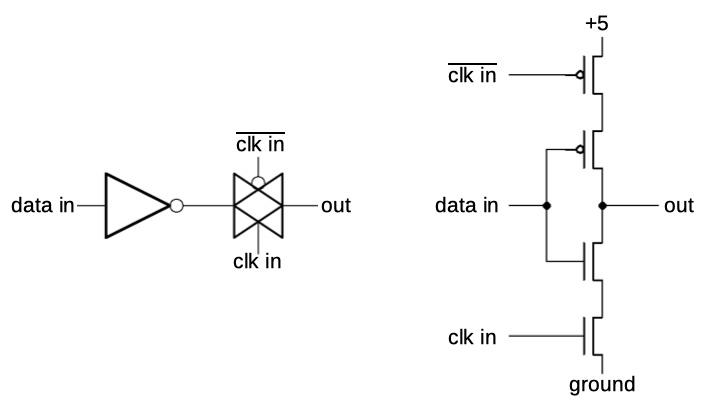
Combined inverter and transfer valve
The photo below shows how one of these valves is made on a chip. The photo shows the metal layer on top. Reddish polysilicon valves are visible underneath. On the left are two P-MOS transistors in the form of concentric circles. On the right are N-MOS transistors.
Conclusion
While the crystal oscillator module looks simple on the outside, there are more components inside than you might expect. There is not only a quartz crystal, but also discrete components and a tiny IC. The IC combines capacitors, analog circuits to provide oscillation, and digital circuits to select frequency. You can select one of four frequencies by changing the IC wiring during production.
More information on crystal oscillators can be found on the EEVblog , electronupdate and WizardTim sites . You can check out the Kolpitz generator on Hackaday .
I'll end with a photo of the chip after removing the metal and oxide layers so that the silicon and polysilicon can be seen. Large pinkish capacitors stand out the most, but transistors can also be considered. Clickable