Lovers of glands - welcome under cat.
Requirements of TK
- Power supply from a three-phase network in case of breakage / disappearance of one or two phases
- Phase voltage 230V ± 20%
- No power factor correction required
- Output power 10W
- Output voltage 15V
Let's calculate in what range of input rectified voltages these requirements pour out. The lower limit is a break in two phases, the phase voltage is 184 V. We get the amplitude of the rectified voltage 259 V. From this value, you need to subtract the dip in the input capacities. Let this value be, say, 59V (be sure to check it later on the breadboard), we get 200V DC, this is the minimum input voltage.
Upper bound. All phases are present, phase voltage is 276V. We get 276 * √2 * √3 = 674V.
Power section
With a power of 10W, the choice of topology is obvious - a flyback converter. In terms of choosing a power transistor, options are possible:
- High voltage switch. We choose a transistor for 800 - 1000 V.
- Cascode inclusion. Series connection of two transistors at a lower voltage. The general principle of this approach is described in the article . There are reference designs such as from Texas and this from Infineon.
Feedback, stabilization method
The following options can be distinguished:
- "Classic" with feedback through an optocoupler. An understandable, widespread scheme, does not require additional comments.
- Power winding stabilization. In this version, the voltage on the feed winding of the PWM controller is stabilized. In this case, the voltage on the output winding is more or less stable. In this embodiment, the quality of stabilization depends on the coupling coefficient between the windings.
- Primary Side Regulator (PSR). A relatively new technology that allows you to achieve the formation of a rectangular characteristic of the power supply (CV / CC). This is done only from the primary side (the optocoupler is not required). Different manufacturers have different variations, but the general principle is based on sampling the voltage from the auxiliary power winding (to ensure voltage stabilization), as well as the key current (to ensure current stabilization). Another feature is that it is often a PFM rather than a PWM modulator.
I decided to choose the classic solutions - take an 800-900V transistor and make feedback through an optocoupler.
Calculation of the transformer
By the way, it should be noted that in the flyback converter this is not a transformer, but a two-winding choke. I write just in case, to inform readers perfectionist that I am aware of and prevent
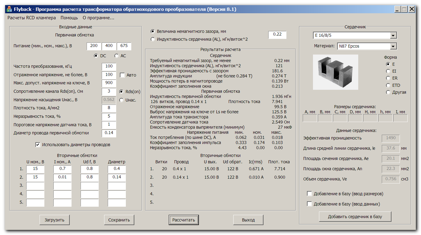
In my practice as a power electronics developer, I use various calculation methods, and often a combination of them. In this case, I use a simple and quick method - calculation using the flyback utility ("Old Man's program") with subsequent verification on the model.
The calculation looks like this:
Some notes and recommendations for the calculation:
- (DCM), (CCM) . – , ;
- ;
- , . , 300-400 . , ;
- 0,5 – ;
- R DSon - we take the nominal value from the DS and multiply by 1.3-1.5 (increase in channel resistance from temperature);
- The current density in the windings can be taken within a fairly wide range. Starting from 5-8 A / mm2 (with natural convection) and up to 15-20 A / mm2 (forced cooling of the power supply or the use of a radiator for the transformer.)
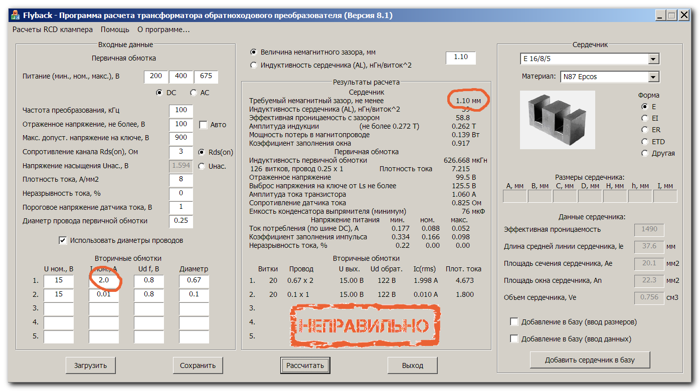
I want to warn novice developers, the utility will not calculate everything for you - it's just a tool that you also need to be able to use. To illustrate, I will give a few examples of unsuccessful calculations.
The reflected voltage is set too low, so the duty cycle is too low:

Too high power is set for the given size of the core, respectively, the gap is too large - the transformer will heat up due to the buckling of the field in the gap, and the leakage inductance will also increase:
Power section simulation
I want to note right away that this is an "ideal model", that is, a model without taking into account parasitic parameters. The field of application of this model is rather narrow - you cannot look at it on the drain on the drain from the leakage inductance, ringing on the output diode and other similar things. What you can use this model for:
- Checking the calculation of the transformer in terms of the duty cycle;
- Calculation of the average and effective currents through the transistor and output diode;
- Calculation of the effective current of the output capacitor;
- Calculation of the effective current of the input capacitor (you need to modify the model by adding a rectifier and an AC voltage source to the input).
The model is available here . Model diagram:
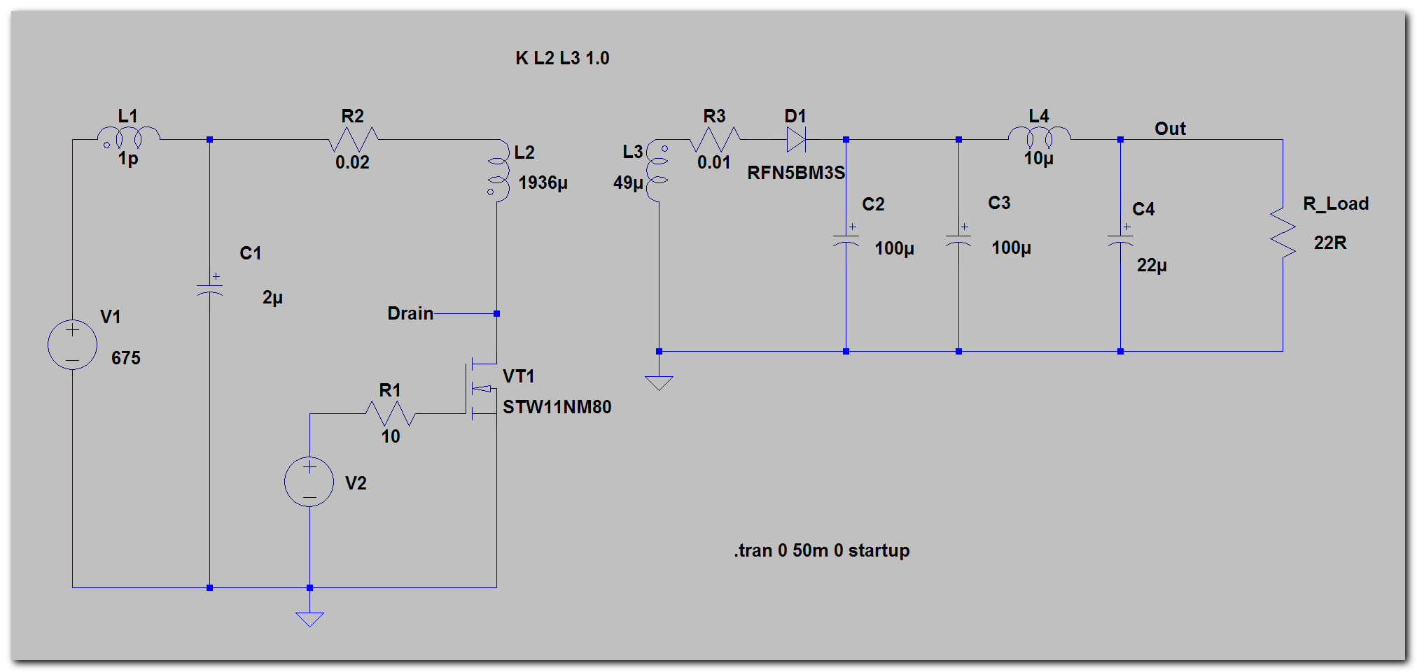
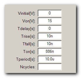
There is no voltage feedback, therefore, to ensure the exact value of the output voltage, the pulse duty cycle must be selected. This is done based on the values obtained when calculating the transformer. With an input voltage of 675V, a duty cycle of 0.103 is obtained, which corresponds to a pulse width of 1030 ns. In the model, I got a value of 886 ns - very close, we can assume that we hit.
Source V2 parameters:
It can be seen that the model uses not the number of turns, but the inductance of the transformer windings. How to determine the inductance of the secondary winding, because its "Old Man's program" does not calculate? Calculate by any method according to the known parameters of the core section, clearance and number of turns. For a quick calculation, I recommend using one very useful utility. Magnetic Design Tool from TDK / Epcos. There is both an online version and a desktop version . I traditionally use the desktop one, because when I started using it, there was no online version yet.
Perhaps when I have time I will write a detailed description of all the capabilities of this tool, but for now, a short guide on how to calculate the inductance of the winding:
- Core calculations;
- Core , Material ;
- Al value;
- s – , ;
- Calculate, Al L-Al;
- N ;
- Calculate L .
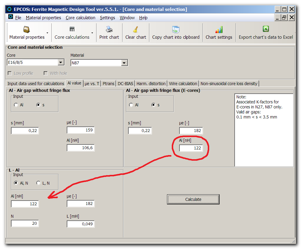
When calculating the parameters for E-shaped cores, the Al - Air gap with fringe flux (E-cores) region is used , for all other core shapes we calculate in Al - Air gap without fringe flux .
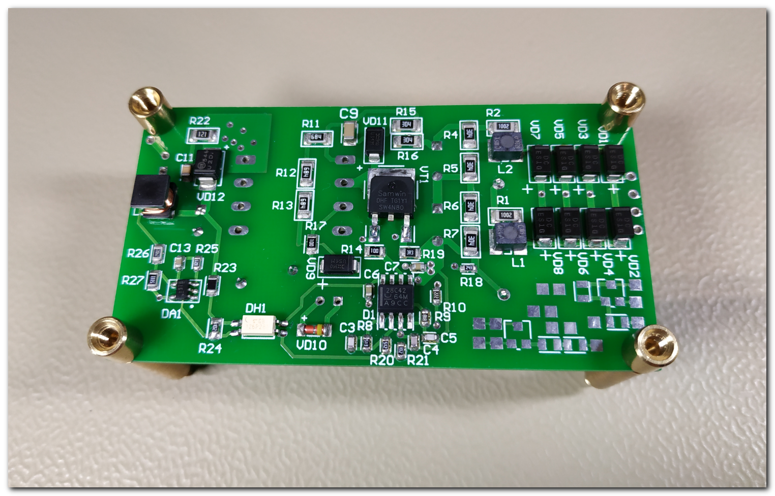
Power supply circuit
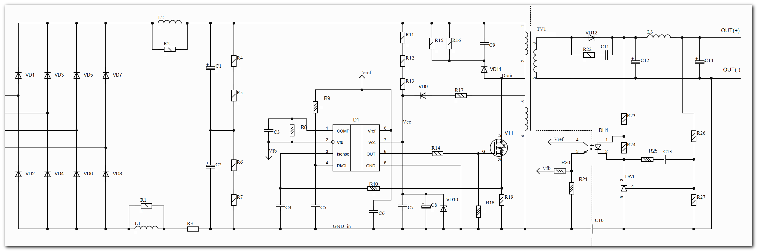
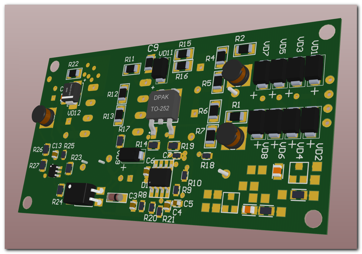
As I said, the scheme is quite classic. There is a point worth noting - the input voltage is quite high, so the input capacitor consists of two connected in series. In this case, it is imperative to use equalizing resistors R4… R7.
As for the printed circuit board - nothing special either, the project is not complicated. However, for products with such a (rather high) voltage, special attention should be paid to clearances. I did not set very large gaps, as I planned to fill with a compound.
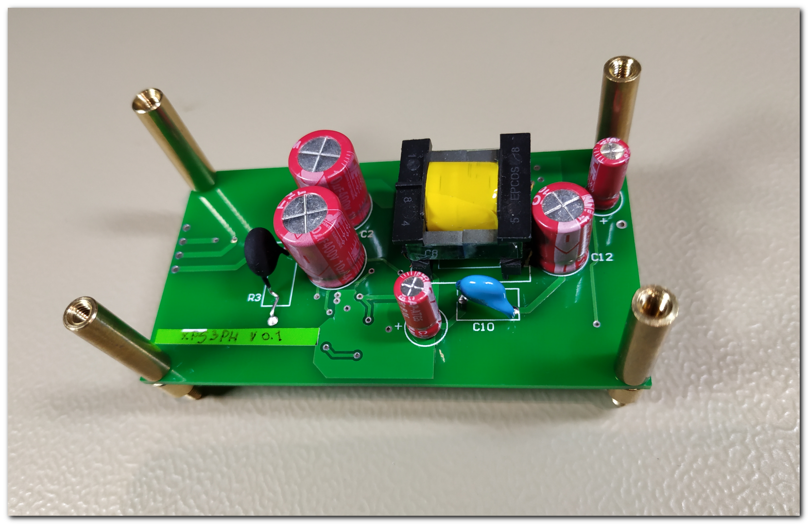
Debugging a power supply
Debugging is the process by which the board turns into this:
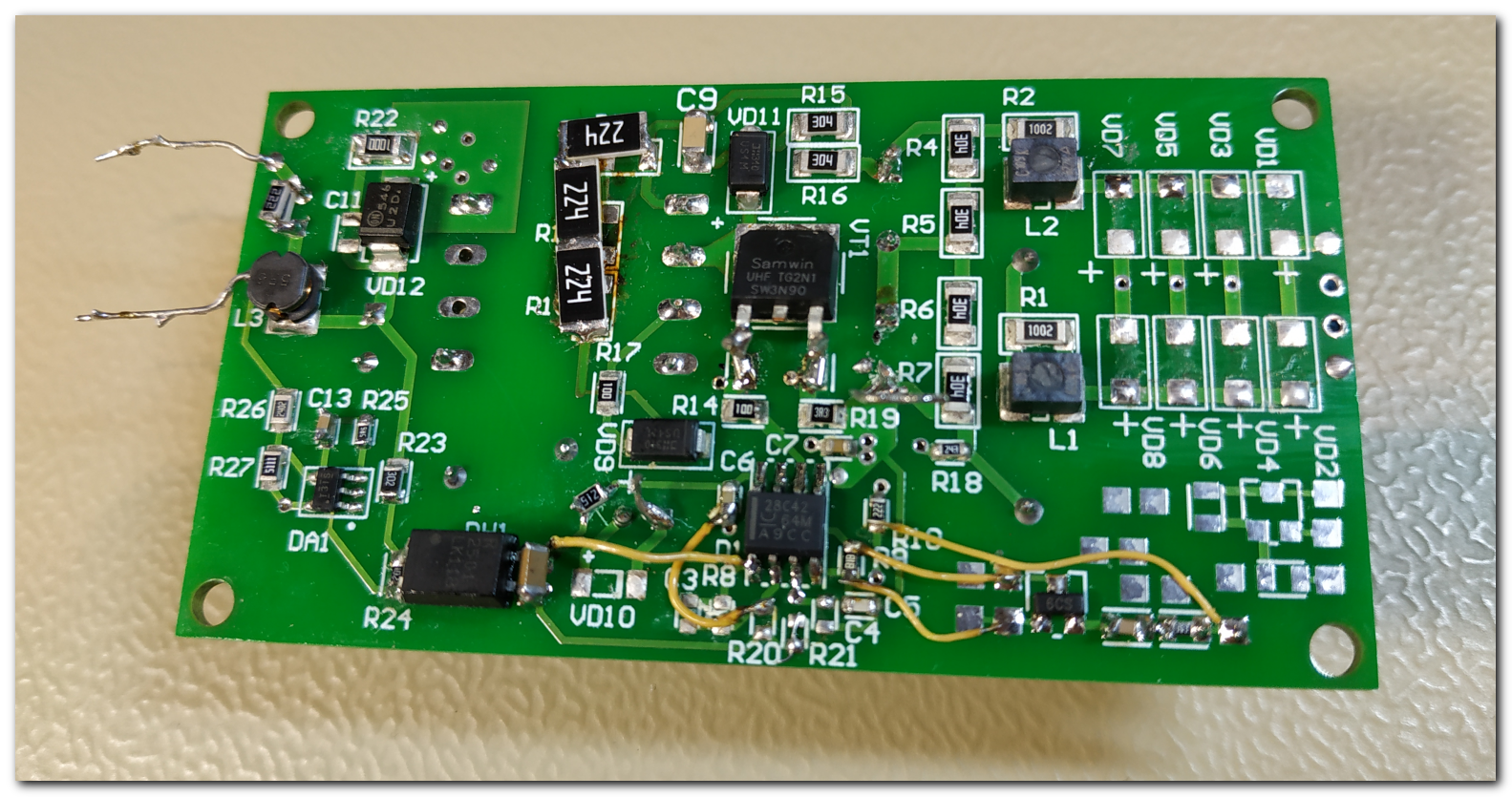
This is of course a joke and it does not always happen (usually even worse), nevertheless, starting and debugging a power supply is a very entertaining topic.
A small checklist that must be done during debugging and preliminary testing. If we talk about critical parameters that can lead to a violation of normal operation, then you need to check:
- Working frequency;
- Voltage at the input when power is applied in a jump (in the presence of chokes at the input, there may be a resonant process and an excess of voltage over the supplied one);
- The voltage at the drain of the power switch at the maximum input voltage;
- The voltage at the drain of the power switch at the maximum input voltage and short circuit at the output;
- ;
- 8 ( – , , );
- ;
- -;
- ;
- ;
- . , – . .
If I forgot something - write in the comments, perhaps with the help of the collective intelligence we will compile a more detailed list of critical tests.
Conclusion
I did not have a goal to describe the entire development process in full - I showed only a few points. If you have any questions about this development - ask in the comments, I will be glad to answer!
Power is cool - deal with it.