From the article you will learn the features of the use of silicon carbide MOSFET transistors and diodes, how to choose an element and a comparison with silicon (Si) devices, and, most importantly, the results of my experiments and research in slowing down the switching of SiC transistors, carried out on my recent development - the source supply for solar energy.
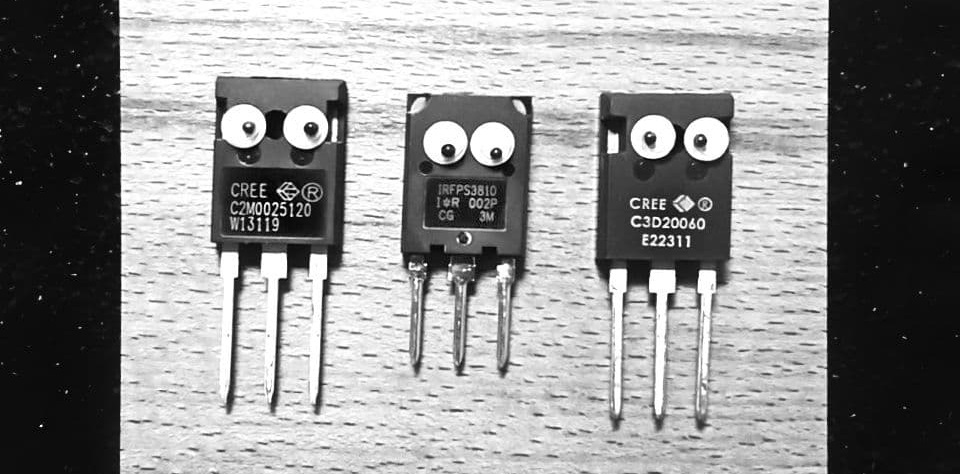
Under the cut a little analytics and practice in the field of power electronics - welcome.
Silicon carbide
Silicon carbide is a wide-gap semiconductor material used in the manufacture of diodes, transistors and thyristors. Silicon carbide entered my practice as a power electronics developer for a very long time. About ten years ago I read an article from Infineon that the use of a SiC diode in a power factor corrector (PFC) can significantly increase the efficiency of the converter. Applied. And even compared it with a silicon diode - indeed, the gain turned out to be very significant. Since then I have applied SiC diodes and transistors in many designs.
Let's see what advantages SiC MOSFETs have over silicon ones:
- (Ciss) (Coss) , ;
- Qg, ;
- RDSon, ( );
- RDSon ;
- ;
- .
In order not to be unfounded, I propose to compare the parameters of a silicon carbide transistor with similar ones based on Si. For comparison, I chose a Wolfspeed (Cree) SiC MOSFET (C3M0060065K), as well as a couple of Infineon transistors of the C7 (IPW65R065C7) and CFD7 (IPW60R070CFD7) families. These transistors are selected from the top families, since they can somehow compete in electrical parameters with silicon carbide.
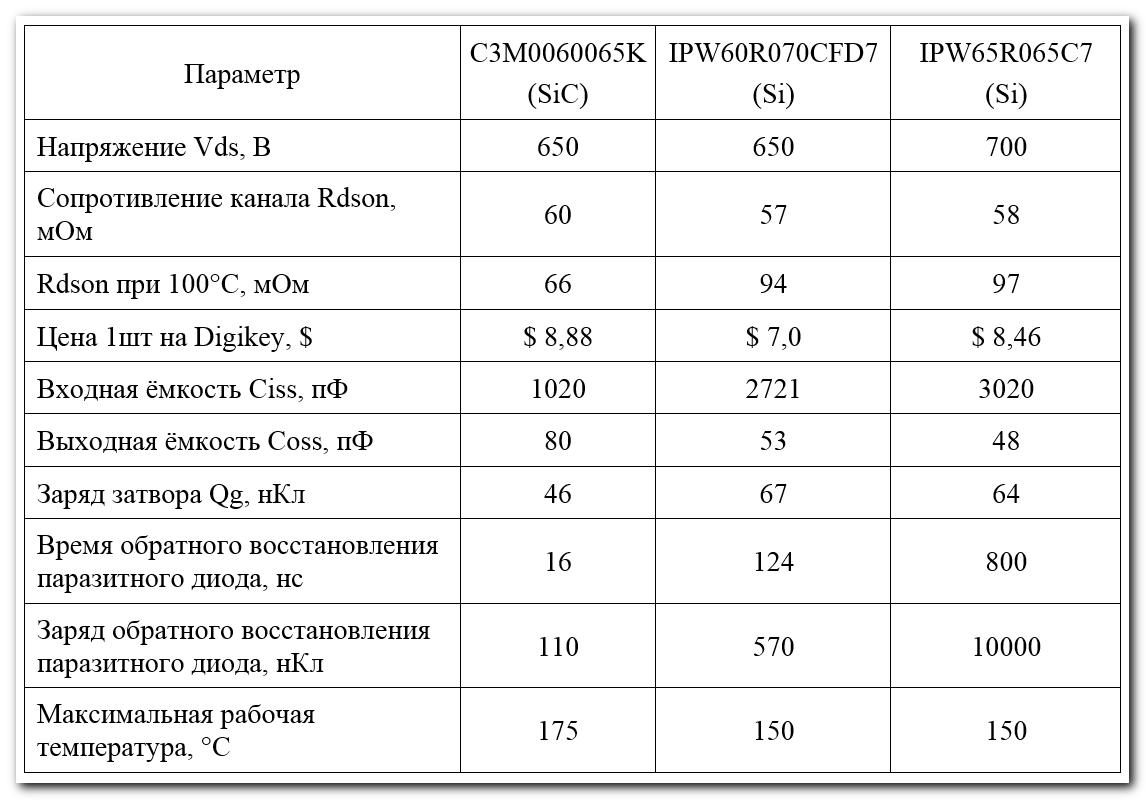
Looking at this comparison, we can say that silicon carbide is superior to silicon transistors in all respects (except for price). A few words about the channel resistance R DSon . Indeed, this parameter for the selected Si transistors is slightly lower for normal conditions, but this is more than compensated for by the very strong temperature dependence of R DSon .
The next picture shows the dependence data for two transistors. It can be seen that at a temperature of 100 ° C (I put dots on the graphs) the excess for silicon carbide is only 10%, and for a silicon transistor 65%.

Power semiconductors never work at room temperature, and the effect of crystal temperature on the forward channel resistance can be quite significant. This feature should always be taken into account when calculating static losses and choosing transistors. The graph shows that even at a temperature of 75 ° C, when calculating the effective R DSon value for silicon, a correction factor of 1.4 must be applied.
We looked at the benefits of silicon carbide, what's the other side of the coin?
What can stop you from using a SiC-MOSFET?
Price. Although the above is a comparison of prices, this is a selection of more or less equivalent PP devices (let's say, top-class). And the problem can be solved with cheaper transistors. For example, NTHL095N65S3HF - an ordinary silicon transistor from ONsemi, 650V, 36A, costs only $ 4.86, and in a batch of 100 pieces it is even cheaper - $ 3.3. It's okay that the channel resistance is slightly higher, it will fulfill its task, it will simply be less than the efficiency of the converter. With a special desire, you can find a transistor from a good Chinese manufacturer for $ 2.5.
Very fast switching. On the one hand, this is a plus - dynamic losses are reduced. But on the other hand - minus, large values of dV / dt lead to an increase in the level of interference, both conducted and radiated. But nobody canceled certification and tests for EMC.
The need for bipolar gate control (active locking). Yes, SiC transistors are now appearing, where the DS says that this is not required. But to be honest, I wouldn't do that for hard industrial applications.
Lack of standards for avalanche breakdown. To be honest, this fact came as a surprise to me. Indeed, these standards (avalanche rating) for SiC transistors are absent in DS. The main vendors are "tactfully" silent, although I managed to find this on the ROHM Semiconductor website .
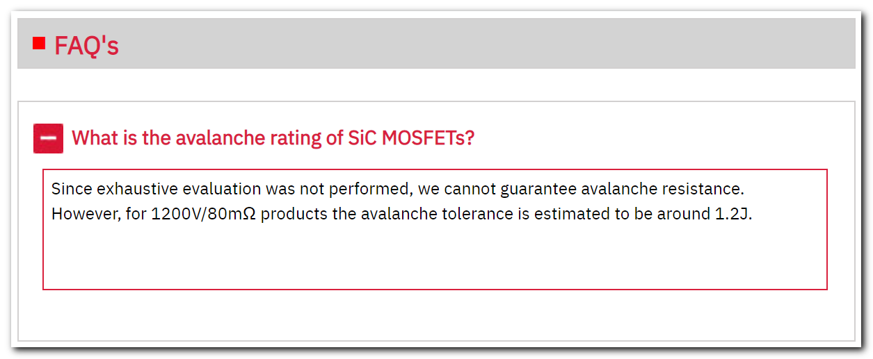
After reading independent studies on avalanche breakdown of silicon carbide, it became clear that this is a real wormhole and, perhaps, a review of this topic is beyond the scope of this article. The only thing that can be noted is that the voltage of the avalanche breakdown of the SiC-MOSFET is significantly (1.5-1.8 times) higher than the boundary drain-source voltage.
A little about silicon carbide diodes
SiC diodes are widely used in power factor correctors (PFC, PFC). KKM is almost always a boost converter, respectively, hard switching and large voltage swing. A fast reverse recovery diode is ideal here. Especially for continuous current mode (CCM) when the switching is energized.
If earlier, when the price of silicon carbide diodes was relatively high, there could be some options, now, without a doubt, put only these excellent diodes in the KKM.
Other applications can also be found, such as high voltage rectifiers.
Study of the SiC-MOSFET Switching Process
When planning the development of a power supply with an input voltage of up to 1500V, I began to study in advance the features of using silicon carbide transistors. I was especially interested in the critical values of the rate of rise of the drain-source voltage (dV / dt), as well as methods for slowing down the switching. We managed to get answers to these questions at the webinar of one of the distributors:

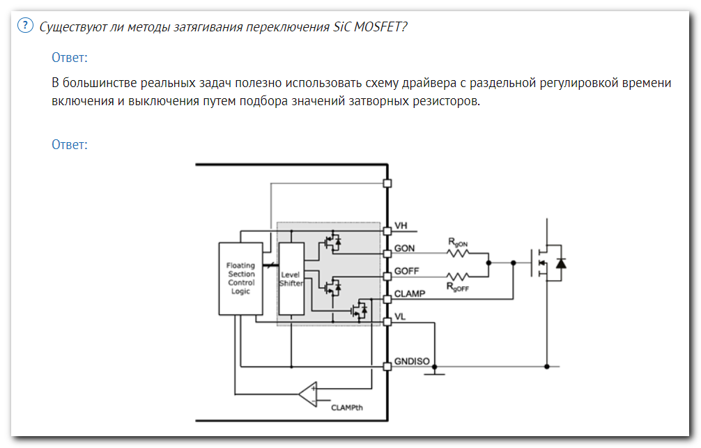
After the first iteration of the converter was built and debugged, I decided to do some research on the possibility of slowing down the switching process. The converter is made in a half-bridge topology, power is 100 W, supply voltage is 750V, transistor control is done according to the following scheme:
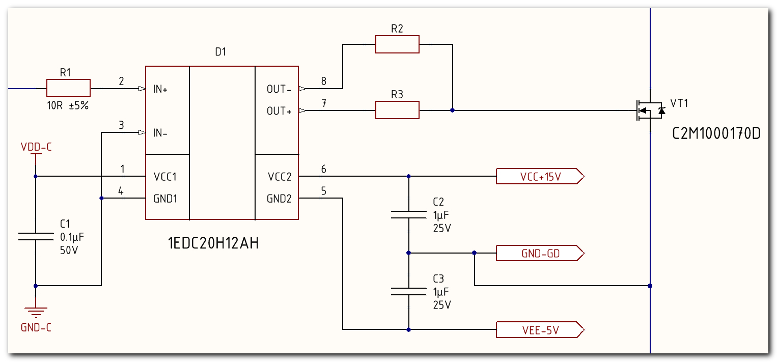
With an increase in the resistance of the gate resistors (R2, R3), the values of the duration of the switching edges were measured, as well as the efficiency of the entire converter. To be honest, I expected that when the fronts were tightened, the dynamic losses would increase and the efficiency would fall. In reality, it turned out differently - the changes in efficiency were not significant. More precisely, when measured using an ammeter built into the power supply, the difference was not noticeable due to the low resolution of this meter. I realized my mistake and measured it again using a more accurate ammeter.
At the extreme points, I got the following values:
- with a gate resistance of 5.6 Ohm, the efficiency is 85.0%;
- with a gate resistance of 330 Ohm, the efficiency is 84.46%.
Thus, the additional power is about 0.5 W. It can be assumed that this is a consequence of an increase in dynamic losses only. Even in this case, we divide by two transistors and we get 0.25 W of additional power dissipation per switch. I would not say that this is a lot. Plus, 330 ohms at the gate is a totally impossible value! To be honest, it was scary to install such resistors (the power supply developers will understand me) and I wonder how the source with an input voltage of 750V did not burn out. But, as they say, what can't you do for the sake of science
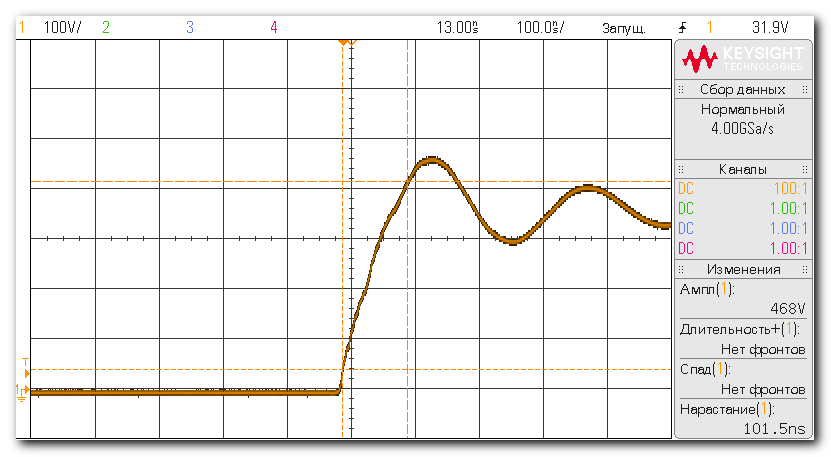
Oscillograms of the drain-source voltage of the lower key with 5.6 Ohm gate resistors:


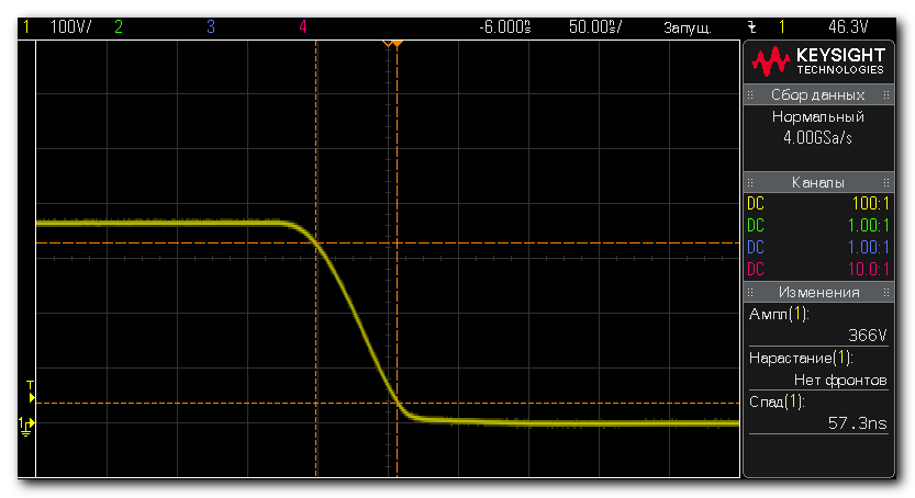
Oscillograms of the drain-source voltage of the lower key with gate resistors 220 Ohm:


Switching times versus gate resistor values:

Of course, I was very interested in what happens at the gate with a 330 ohm gate resistor. Miller's shelf was not that huge:

Conclusion
Let me remind you that the object of the study was a 100 W power supply with an input voltage of 200-750 V (DC). Output voltage 24V. Topology - half bridge. Power transistors C2M1000170D (silicon carbide).
So, the highest obtained slew rate of voltage at the drain is 18 V / ns, which is significantly lower than the limit values of dV / dt 100-150 V / ns.
An important conclusion that can be drawn from these studies is that delaying the switching fronts of silicon-carbide transistors by increasing the gate resistors is not particularly effective. In my opinion, in a real design, you can afford to install a 22 ohm gate resistor, well maybe 47 ohm in some cases. It can be seen from the results of the study that at such values, there is no significant drag of the fronts.
Regarding the use of silicon carbide semiconductors - SiC must-have diodes in any PFC (if there are no really strict price targets), as for transistors, I have deduced for myself several conditions under which they should be used:
- high input voltage of the converter (500-1500V);
- elevated ambient temperature or poor cooling conditions;
- increased compactness of the solution is required (accordingly, we choose a higher frequency);
- high efficiency is required;
- I want to
feel coolto try new power electronics technologies.
You can use my recommendations or come up with your own. In any case, let your developments be efficient and reliable! And, until we meet again.
Power is cool - deal with it.