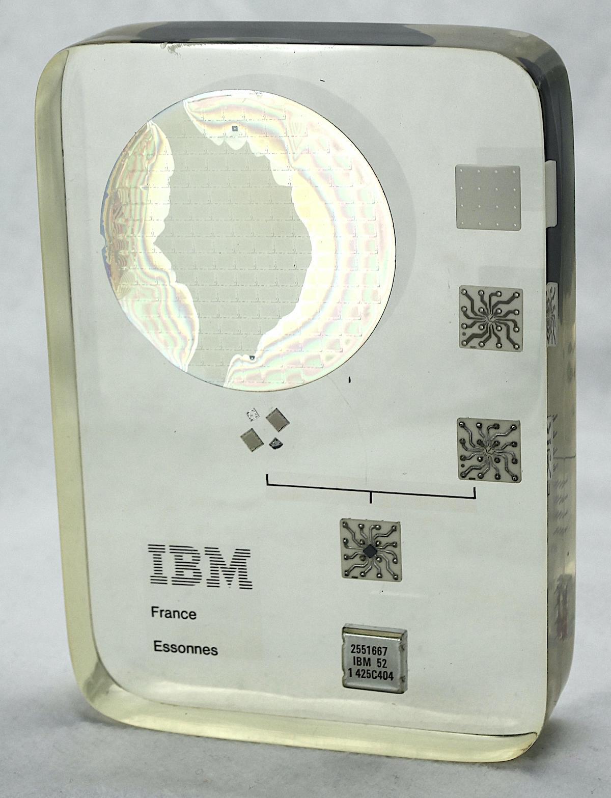
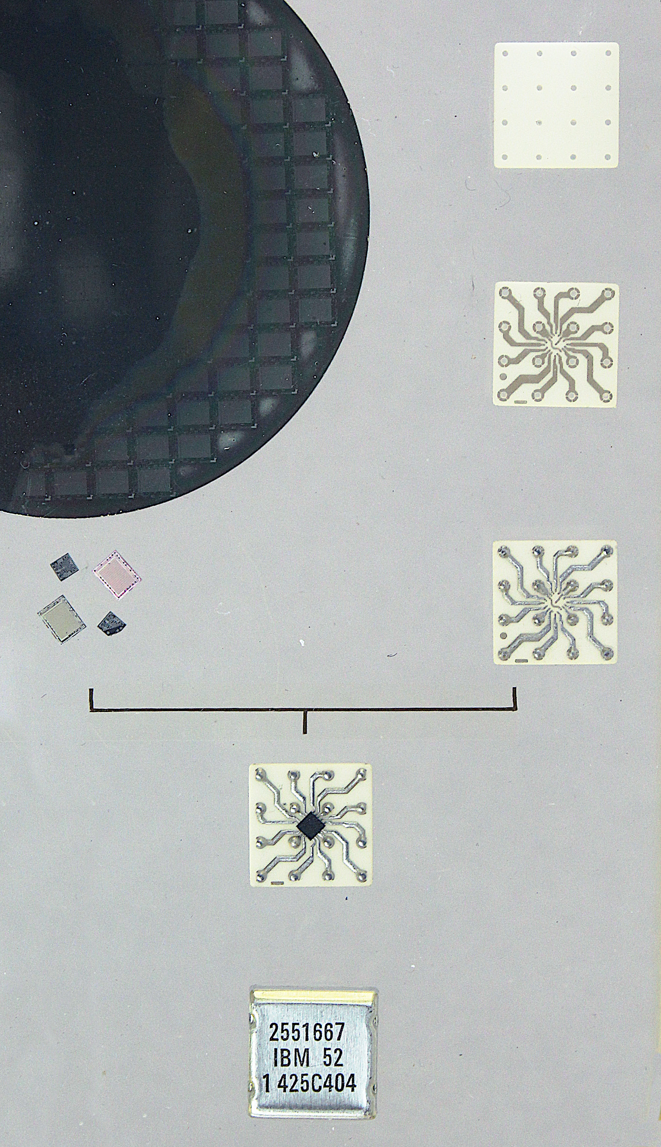
When IBM began using integrated circuits in the late 1960s, the chips were packaged in square metal modules called Monolithic Systems Technology (MST). The paperweight presents several steps in the production of an MST module. The silicon wafer is cut into crystals, mounted on a square ceramic support, and wrapped in a thumbnail-sized metal case.
- , MST- . - .
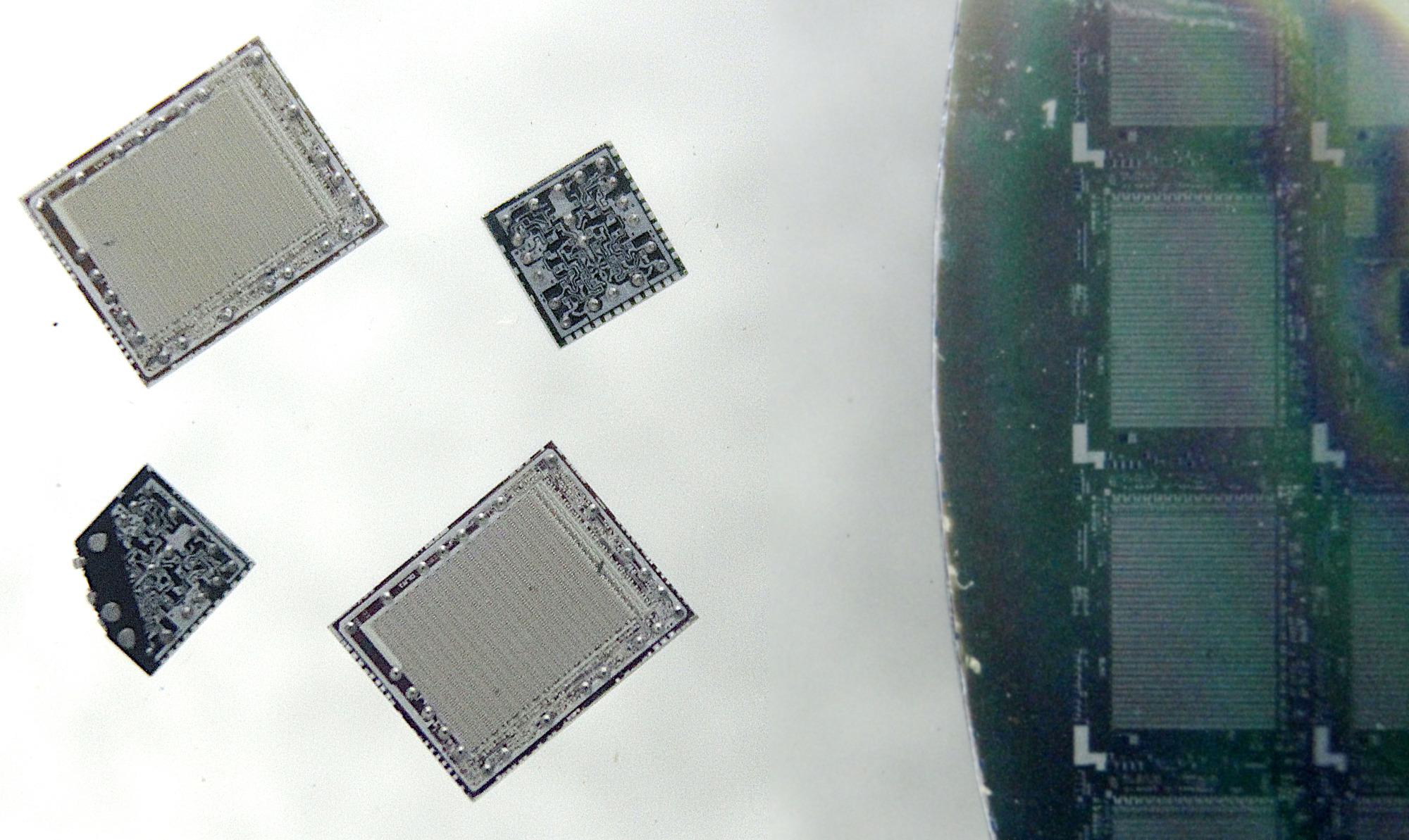
Crystals are enclosed in plexiglass, so you can study their schemes in detail and better understand the methods of work. The photo below shows an enlarged image of the edge of the silicon substrate and four crystals enclosed in a paperweight. Two large crystals are the same as the crystals on the base. Two small ones are the same, but one is damaged.
I wonder why one of the crystals is missing an angle. However, it is not just chipped off - the metal layer and silicon do not reach the edge. Probably, this crystal was on the edge of the substrate and did not go through the production cycle to the end. It follows that the company used rejection to make such paperweights.
Damaged crystal
For this article, I photographed the crystals under a microscope and reverse engineered the small chip. I concluded that large chips are 1Kbit static memory chips, and small chips are memory read amplifiers.
IBM System / 370
These chips are likely used in the popular System / 370 mainframe line. In 1964, IBM introduced the System / 360 family of mainframes, which proved extremely popular. In 1970, it was redesigned with the announcement of the System / 370, which was assembled from integrated circuits (as opposed to System / 360) and moved from magnetic core memory to semiconductor memory . The paperweight contains both major changes: the integrated circuit and semiconductor memory.
To give you an idea of the scale of a System / 370 computer, here's a rendering of a System / 370 Model 145 computer. The Model 145 was a "mid-size" machine in the System / 370 line.
For a time, IBM used a logical numbering system for the System / 370 line - as the number increased, so did the power. The range of models ranged from the most feeble Model 115 to the most powerful Model 195. However, in the late 1970s this numbering system collapsed , and the models began to be called seemingly random numbers - 3031, 4361, 3090 and 9370. At the same time, Model 9370 was the least powerful.
The Model 145 was the first computer from IBM to have semiconductor main memory. This computer was very large by modern standards - in the image below, it occupies all the blue cabinets. In one cabinet there is a processor, in another - 256 kB memory chips. There were no microprocessors at that time, so its processor is assembled from many printed circuit boards, on which integrated circuits are located. The Model 145 weighed over a ton, cost $ 5-10 million (in today's prices), and was about the same speed as the 1981 IBM PC.
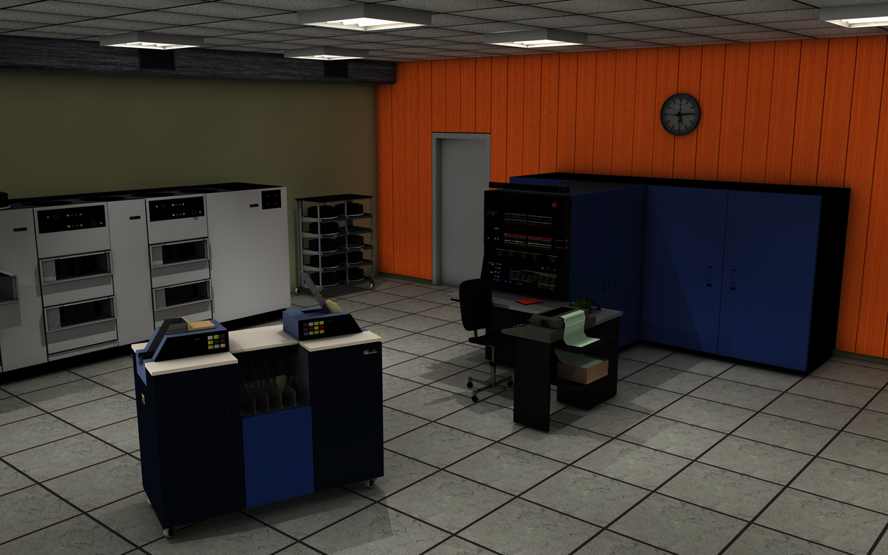
Computer render System / 370 Model 145. Computer - in blue cabinets. White cabinets in the back are disk drives. In the foreground is a card reader.
MST modules
In the early System / 360, IBM used SLT hybrid modules instead of integrated circuits (ICs). For the System / 370, the company switched to ICs, calling them "monolithics." Most companies packaged ICs in square plastic or ceramic cases, but IBM kept the rectangular cases from SLT and called them MST - Monolithic Systems Technology.
IBM had different MST logic options for different products. Different versions used different voltages. MST-1 used ground as the high voltage threshold, -4 V as low, and -1.32 as the ESL voltage reference ... Since ECLs are sensitive to high voltage fluctuations, often chips of this family used ground as the upper voltage, and the lower voltage was negative. For the MST-2, the levels were shifted so that the reference voltage became equal to ground, the upper voltage was + 1.25 V, and the lower one was –3 V.
The MST technology was a significant breakthrough compared to the hybrid SLT. It was ten times more reliable and 4-8 times more dense. In modern terms, the MST ISs were extremely simple. 32 transistors in one module implemented about six logic gates, so thousands of ICs were required to implement a whole computer.
The MST modules were manufactured in large quantities by automating the production technology. The sequence of components enclosed in a paperweight demonstrates the manufacturing steps. On the left is a round silicon substrate that is cut into individual crystals. On the right is a square ceramic base with 16 pin holes. Then a printed circuit is applied to the base, connecting the IC to the contacts.
The ceramic base of the MST provides an interface between two circuit scales - a PCB with 0.125 "spacing between pins, and an IC with 0.01" spacing between balls. The ceramic-based circuit has interesting features. Each power pin connects to three balls, allowing more current to be supplied to the IC. The V- track crosses the chip, giving two pins to connect on both sides. The V + track runs to the center of the chip, providing additional pins for power.
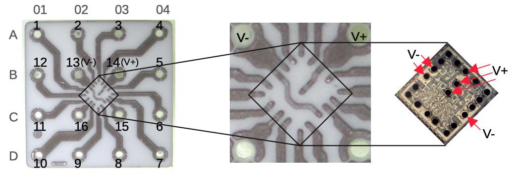
For some reason, MST uses two different pin numbering schemes. For SLT, the contacts were numbered in a spiral leading to the center. But on MST, the numbering from A01 to D04 is more common.
In the third step, 16 contacts are soldered to the base. Then the silicon crystal and ceramic base are combined. The crystal is placed upside down in the center of the ceramic base. See how much the crystal is smaller than the case. The module is soldered by melting the dosed solder, the contacts of the silicon crystal are directly soldered to the base.
IBM called this technology " controlled-collapse chip connections ," or C-4. A controlled amount of solder was used to make the contacts in the module. During soldering, the chip was pulled up to the fingers of the module by surface tension - much like surface mounting is done today.
Finally, the module was inserted into a metal case, and a square chip with a half-inch side was obtained. These modules had a distinctive appearance that differed from the ceramic or plastic DIPs used by other manufacturers.
Stages of MST production MST
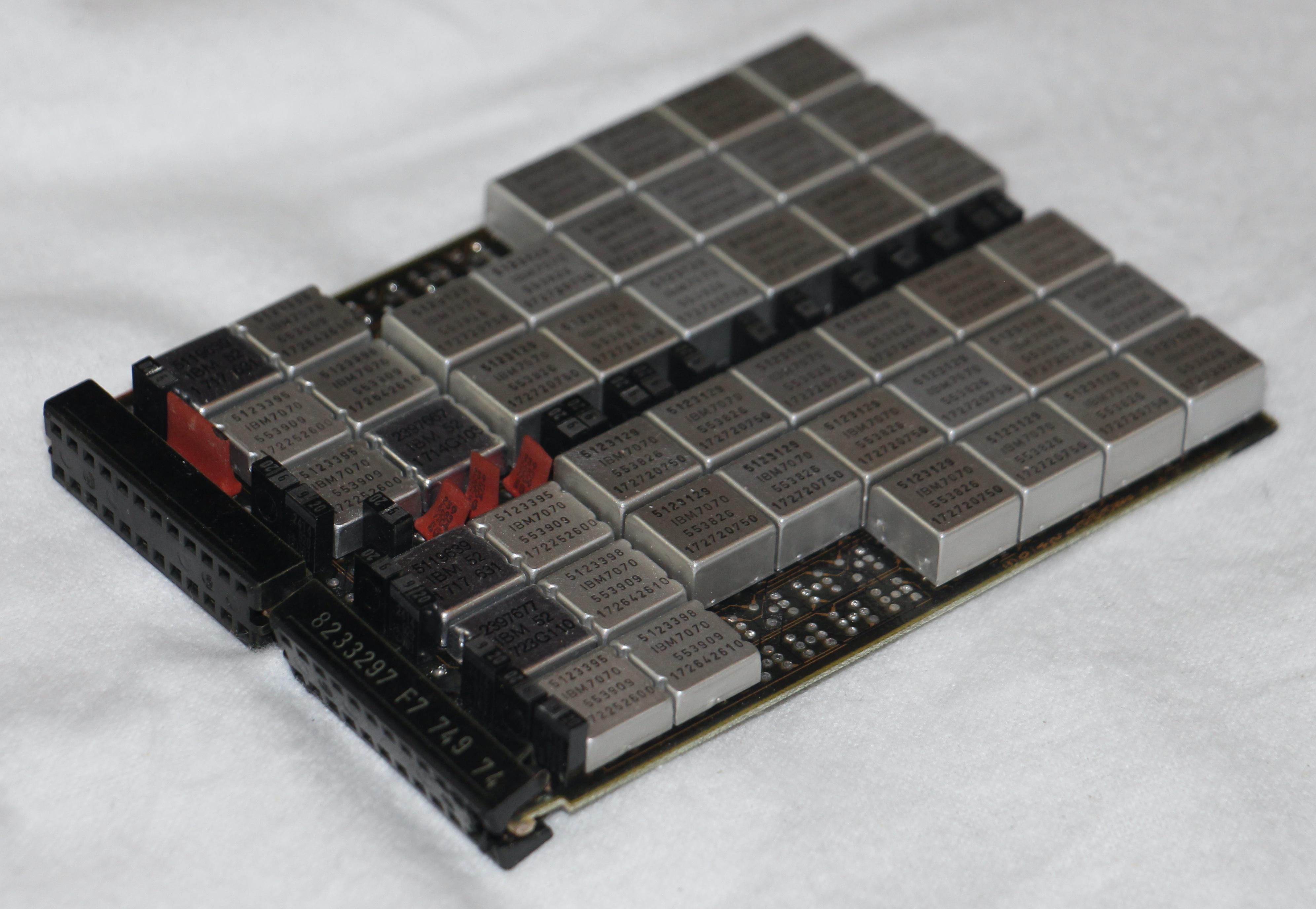
modules were tightly placed on boards - see, for example, the photo of the memory card below. Square modules, together with a four-layer board, produced a significantly higher density than other PCB manufacturers of the time, using DIPs and double-layer PCBs.
Memory card from IBM
Substrate and memory chip
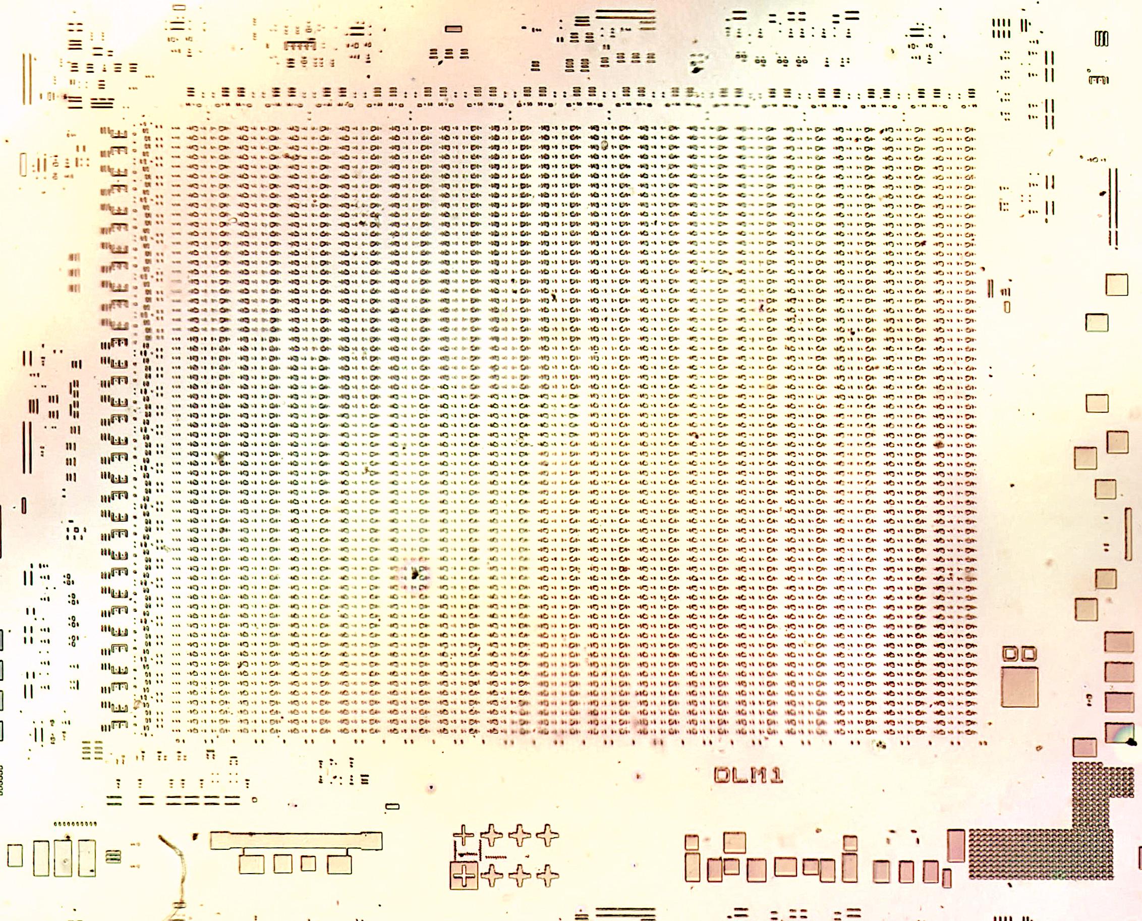
Inside the paperweight is a silicon wafer with a diameter of 50 mm - this size was introduced in 1969. Since then, the dimensions have increased steadily, and modern manufacturing uses 300 mm diameter substrates. There are 177 crystals on the substrate - I took a photo of one of them under a microscope (see below). Interestingly, this substrate is not completely finished - apparently, only one level out of nine is applied. The photo shows test outlines and alignment patterns between crystals.
The photo shows the article DLM1
The paperweight also contains ready-made crystals, the photos of which are given below. A lattice of memory cells is visible in the center of the chip, and auxiliary contours are located along the edges. After examining the crystal and counting the cells, I decided that it was a kilobit static RAM. Ball leads are visible along the edges of the crystal, allowing the chip to be soldered directly to the ceramic base. There are 25 of them, respectively, the chip was most likely mounted in an MST case with 5 × 5 pins.
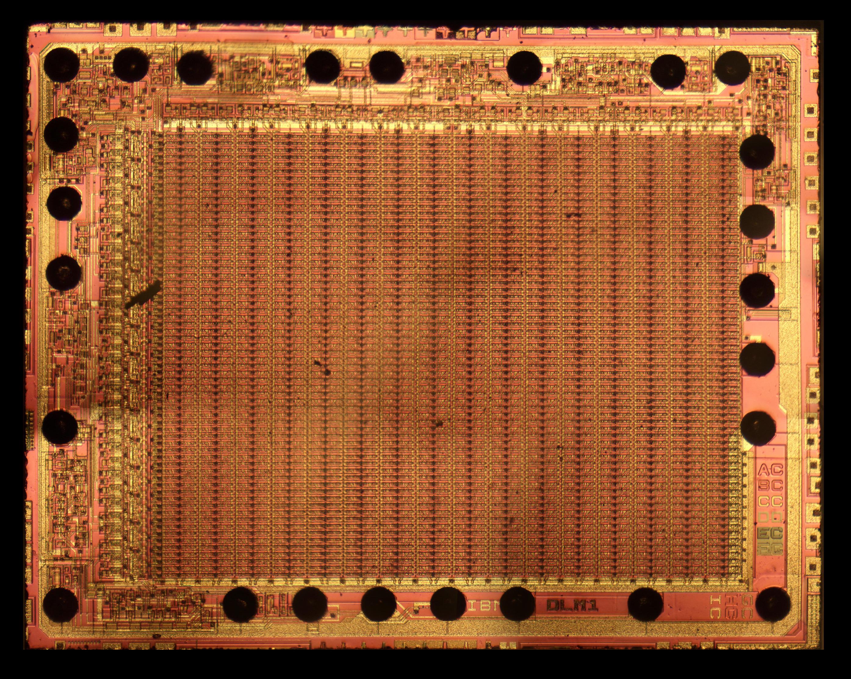
Memory Chip
It is difficult to photograph modules enclosed in plexiglass under a microscope, so at high magnification the chip circuits are not visible, and I could not carry out its reverse engineering. I was able to measure the characteristic size of its parts - 6 microns. Such a technical process appeared in 1971.
The photo below is the best resolution I could get. I think these are six memory cells - I have framed one. I think these are two cross-linked inverters, a standard static RAM cell circuit.
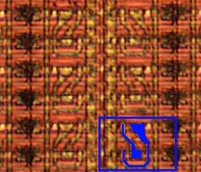
Memory readout amplifier chip
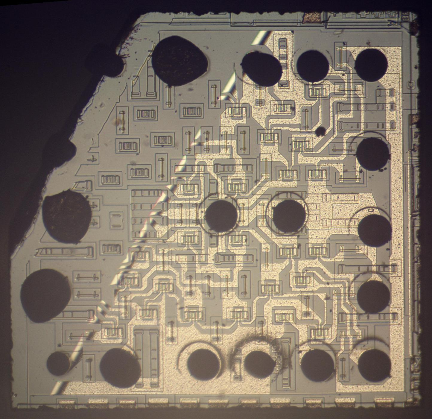
A small chip in a paperweight is much simpler, and its components are much larger. Below is a photo I took. I found 32 NPN transistors and resistors on it. The chip is partially analog and uses ECL . I think this is a different type of amplifier - a readout amplifier for signals from a memory chip. This explains why it is these two chips that are enclosed in the paperweight.
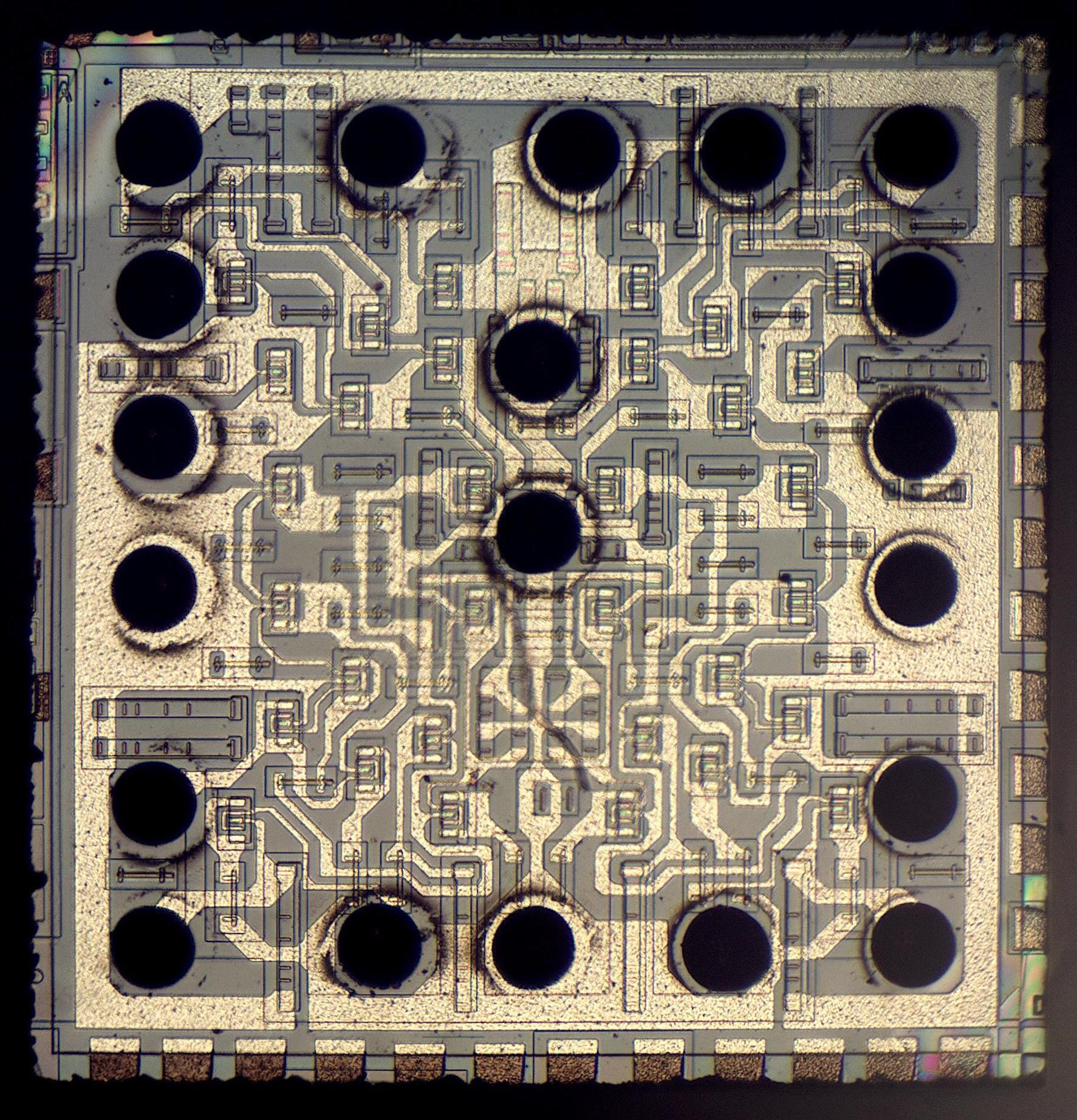
In the photo, silicon is gray. Parts of silicon are dopedarsenic, boron or phosphorus to obtain areas with different semiconducting properties. Black lines are boundaries between different levels of impurities. Yellowish - metal conductors on top of silicon, connecting the various components. The large black circles are the ball leads connecting the die to the MST substrate.
Below is a diagram of a part of a chip that shows two types of resistors and a transistor. The top resistor consists of a high-resistance N-type silicon piece with metal contacts on each side. It turns out a 65 ohm resistor. The bottom resistor has six pins, and the resistance value depends on where the wires are connected. It uses P-type silicon, receiving resistance in the hundreds of ohms.
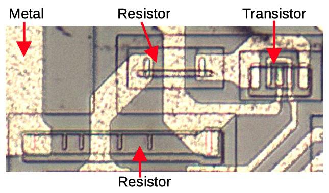
Transistors - bipolar NPN, however, their structure is more complex than that of a typical NPN transistor. Physically they have two bases and two collectors, connected together to reduce the current density. Therefore, each transistor has five metal contacts. The diagram below shows a cross-section of the structure of a transistor. The five metal pins on top correspond to the five pins of the transistor in the photo above. The collector, base and emitter are connected with NPN layers. The P + ring provides circular insulation.

More detailed structure and dimension of transistors:
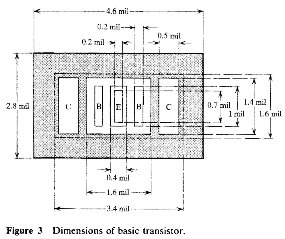
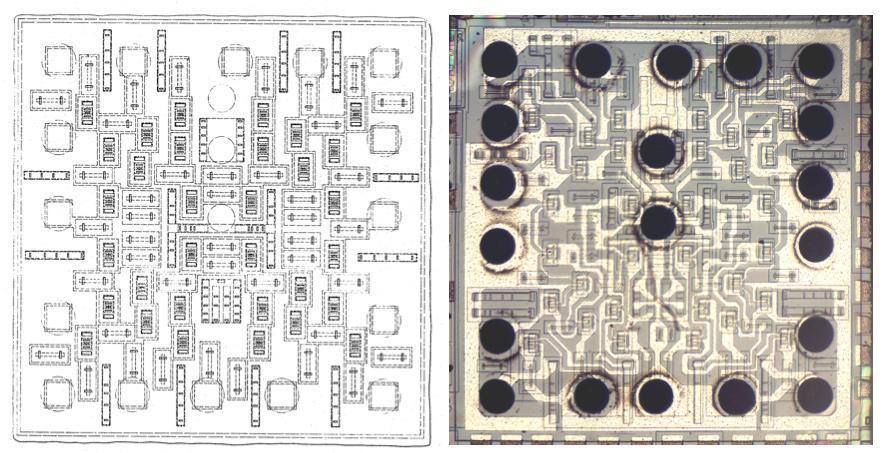
By recognizing the crystal components and understanding the wire connections, you can reverse engineer the circuit. However, if you carefully examine the crystal, you can see that many components are not connected. This is because IBM has used master slice technology to produce many different ICs without having to develop each one individually. The company came up with the idea of using a common silicon crystal with many transistors and resistors. By making a relatively inexpensive change to the metal layer, it was possible to connect the existing components in a suitable way. Therefore, resistors have several contacts for connection - they can be connected in such a way as to obtain different resistance values.
The "master cut" approach used a fixed arrangement of transistors and resistors, and only changed the metal wiring between them during the so-called process. "Personalization". The diagram below is a drawing from patent 3539876, which shows the layout of the components used in the IC from IBM for master slices. If you compare the transistors and resistors, you can see that the circuit is almost completely the same as the paperweight crystal. But there are also differences. In particular, the crystal has additional contacts on the left and right, and the location of the resistors is slightly changed because of this. A paper from 1966 describes where the "master slicer" system came from. As early as 1966, they used computers to design chip circuits.
Differential amplifier and emitter-coupled logic
Logic circuits can be arranged in a variety of ways. Nearly all computers today use the CMOS (Complementary Metal Oxide Semiconductor) logic family, whose gates are composed of MOSFETs. However, the IBM System / 370 used a high-speed logic family called "emitter coupled logic" (ECL), which IBM then called the "Current-Switch Emitter Follower" (CSEF). ECL was invented by IBM in 1956 for use in high-speed transistor computers.
For the most part, ECLs worked quickly because the transistors did not turn on completely (not fully saturate). Thanks to this, the transistors could very quickly switch the path of the current. In addition, the difference between 0 and 1 voltages was small (about 0.8 V), so the signals quickly switched between them. For comparison, for TTL valves this difference was in the order of 3.2 V. Signals usually switch between levels at a rate of about 1 V per nanosecond, so the greater the difference, the longer the switching. On the other hand, due to the small difference between the voltages, the ECL was susceptible to interference .
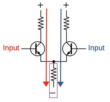
ECL is based on a differential amplifier- a circuit that amplifies the difference between two input signals. It works like this (see diagram below). A fixed current flows through the circuit. If the voltage at the left input is greater than the voltage at the right, the left transistor turns on, and most of the current will go through the left branch (red). Conversely, if the voltage at the right input is greater than the left, the right transistor turns on, and most of the current will go through the right tap (blue). This differential pair provides amplification because a small difference between the input signals produces a large change in current.
This circuit is used in the chip as an amplifier, but after minor modification it also forms an ECL gate. To obtain a gate, the voltage in one of the branches is fixed, becoming a reference, at a level somewhere between the values "0" and "1". If the incoming signal is greater than the reference, it is considered "1", and below - "0". (The MST chips used ground as the voltage reference). An ECL based inverter is shown below - if the input signal is high, the current through the left resistor will pull the voltage down. To increase the speed, the lower resistor is replaced with a current sink (purple). The drain current is controlled by an external bias voltage.
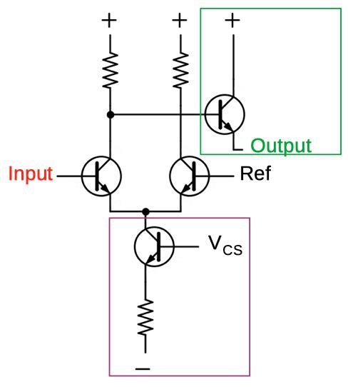
A buffer (green) has been added to the output. The buffer is called an emitter follower because the output is taken from the emitter of the transistor and the output follows the input.
Readout amplifier circuit
I reverse engineered the chip and found that it contained two copies of the schematic below. This circuit is a differential amplifier. It was probably used as a readout amplifier to amplify signals coming from memory chips and convert them into logic ones.
I carefully looked for information on this chip in the documentation, but did not find anything, so I had to study the chip by reverse engineering. At first I thought it was a normal logic gate. However, the two-stage amplification made no sense. Another use case for such a chip is the conversion of differential signals into ECL signals. This would explain differential inputs, but not bi-amplification.
Intel also made chips that required external readout amplifiers - Intel 1103 and Intel 2105 . To do this, Intel released the 3208 and 3408 Hex Sense Amplifiers chips. One reason for the need for external sense amplifiers is that memory chips are made with MOSFETs, and amplifiers are better made from bipolar transistors. Later, readout amplifiers began to be made directly on chips.
The chip has two inputs, negative and positive, and a logic output. Differential amplifiers are the heart of the chip. The incoming signals are buffered and then passed to the lower amplifier (green). The output from it goes to the upper amplifier. This cascading arrangement of amplifiers increases the sensitivity of the chip and provides a greater degree of amplification.

In the yellow boxes - buffers using the previously described emitter follower of the current switch. There is a buffer for each input and output. In the purple frame is the ECL valve. I think it captures the value of the amplifier by sending the output back inward. The current drain transistors are marked in blue. They provide constant current to differential amplifiers and other parts of the circuit.
Conclusion
Quite a long article turned out for a paperweight. However, this subject gives us an interesting glimpse into IBM technology from 1974.
At least I think this is technology from 1974. General considerations allow us to attribute it to the period of the early 1970s. The module has a code "1 425C404". I think that the second number, "4", indicates the year of manufacture. IBM modules are usually marked with three lines of text, but there is no clear information on the meaning of the numbers. The first line is the article. The second is believed to represent the location of the manufacturing facility ("IBM 52" should stand for "Eson, France"). The third line is the date and party.
Among other things, this technology demonstrates IBM's move to ICs and semiconductor memory in System / 370 mainframes. She also explains a unique technique for assembling ICs on a ceramic substrate in a square metal package - MST. Finally, the kilobit memory chip demonstrates the amazing progress that has been made in memory technology over the past decades, leading to the emergence of megabit, and now gigabit chips.