The history of storage is a race between storage and processing power. On the way to computer nirvana, there is a bottleneck - the storage of billions of zeros and ones. The newest player in this field is Non-Volatile Memory Express (NVMe), which is something like a hybrid of several previous technical solutions.
The first generation of home computers used floppy disks and compact cassettes as storage devices but as computers grew, so did the importance of storage. By the 1990s, hard drives became widespread, allowing you to store first megabytes, and then gigabytes of information. As a result, the need for a fast communication system between the drive and the rest of the system has grown. At that time, the ATA (IDE) interface was most commonly used in Programmed Input-Output (PIO) mode.
As a result, technologies have moved to direct memory access (DMA), UDMA, also known as Ultra ATA and Parallel ATA, and SCSI-based interfaces in Apple computers and most servers. As a result, Parallel ATA became Serial ATA (SATA), and Parallel SCSI became Serial Attached SCSI (SAS). SATA was primarily used in laptops and desktops before the arrival of NVMe and solid state drives.
All of these interfaces were designed to keep up with storage devices. In this sense, NVMe is out of the picture with its integration into the system. NVMe also differs in that it is not tied to any specific interface or connector, which can be confusing. Who can separate M.2 and U.2, let alone which protocol the interface uses, be it SATA or NVMe?
Let's understand the wonderful and strange world of NVMe.
Deceptive appearance

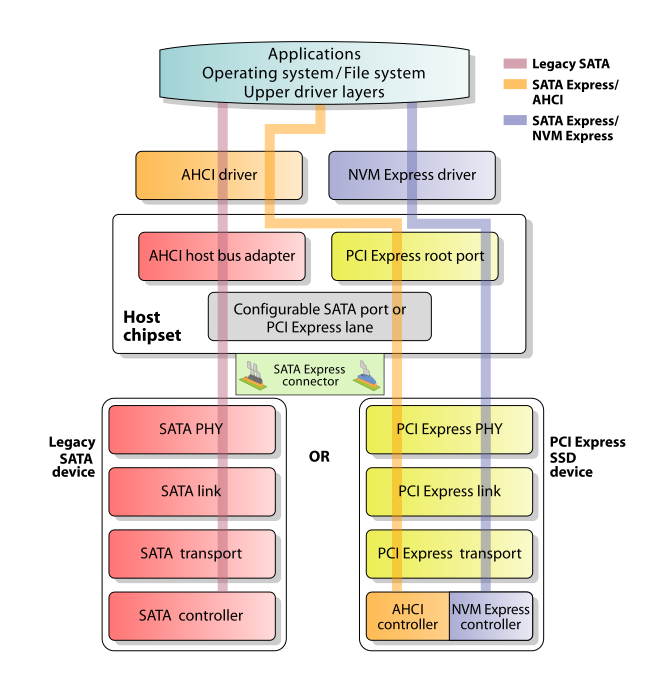
SATA Express elements, functionally similar to M.2.
Ask anyone to show you the NVMe slot on the motherboard and you will most likely be shown a picture of the M.2 slot as it has become the most popular solid state drive (SSD) in consumer electronics. At the same time, even an M.2 slot with a solid state drive inserted into it may not belong to NVMe, since this interface also uses SATA.
The board next to the M.2 slot often indicates which technology it supports. It's also a good idea to read the instructions for the motherboard. The reason for the confusion is that initially there was a Mini-SATA (mSATA) standard for TTN, which used the PCIe Mini Card form factor, which later evolved to the M.2 form factor and the U.2 interface. The latter is more like SATA and SAS interfaces, and combines two channels, SATA and PCIe, into one interface for connecting TTN.
In the meantime, the M.2 standard (after a short excursion into the short-lived SATA Express standard) was expanded in order to support not only SATA, but also AHCIwith NVMe. Therefore, M.2 slots are often incorrectly referred to as "NVMe slots", when in fact NVMe is a PCIe-based protocol that does not define any form factors or connector types.

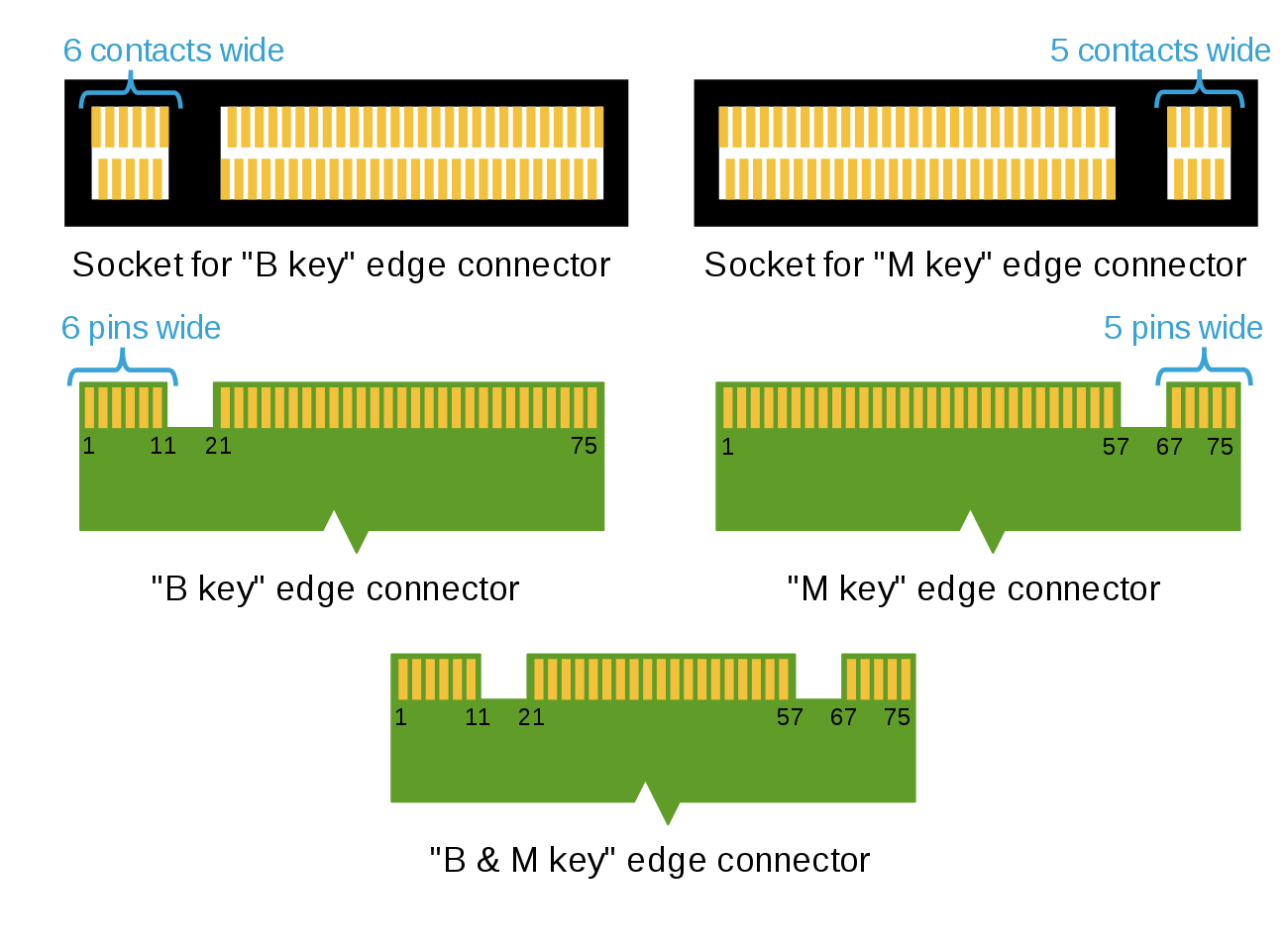
M.2 interface with B and M keys
In the meantime, the M.2 form factor itself is quite versatile - or confusing, it’s like anyone. Physically, it can be 12, 16, 22 and 30 mm wide, and support lengths from 16 to 110 mm. On the edge of the slot, a series of labels are applied to indicate functionality and match the labels on the slot itself. Most often these are labels B and M from the list of key labels, which, for example, contains the following:
A: 2x PCIe x1, USB 2.0, I2C and DP x4.
B: PCIe x2, SATA, USB 2.0 / 3.0, audio, etc.
E: 2x PCIe x1, USB 2.0, I2C, etc.
M: PCIe x4, SATA and SMBus.
It turns out that the physical size of the M.2 expansion card is as many as 32 pieces, and this is even before we take into account 12 possible modifications from the list. Fortunately, the general industry seems to have adopted a common 22mm wide standard for storage cards with limited lengths. As a result, NVMe TTNs are marked as "2242", which means 22 mm wide and 42 mm long. TTN cards can be marked with the letters B, M or both.
It is important to note that today M.2 slots are actively used as PCIe expansion in cramped conditions. Therefore, WiFi cards are often in the M.2 form factor.
Defining NVMe
All of this leads us to the basic definition of NVMe: it is the standard interface for direct-attached PCIe drives. It differs from SATA in that the former converts the PCIe protocol to the SATA protocol, which then has to be interpreted by a special chip on the drive before any commands related to data storage can be executed.
Instead, NVMe defines an interface that can be directly used in any OS that has an NVMe driver. Commands are sent to the NVMe drive, which performs them for reading or writing or performing some kind of maintenance operations such as TRIM... Because any device that claims to be an NVMe device can be relied upon to be a TTN (NAND Flash, 3D XPoint, etc.), the NVMe protocol is designed with low latency and high packet transfer rates in mind.

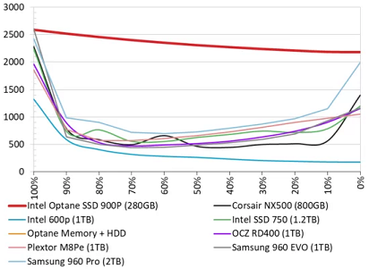
Optane SSD from Intel like 3D XPoint works smoothly regardless of workloads
Recently such NVMe feature as a local memory buffer, Host Memory Buffer ( HMB ), gained popularity . This is an attempt to get rid of the need to buffer data in DRAM using NAND Flash type TTN. The feature uses part of the system memory as a buffer, while losing relatively little in performance, while the buffer is mainly used to cache the address table.
In the long run, given the pace of storage development, technologies such as 3D XPoint make even such tricks unnecessary. The access speed to the same 3D XPoint is closer to DRAM than to NAND Flash. Since TTNs like 3D XPoint do not need a DRAM buffer, their increasing popularity may lead to the fact that NVMe will already be optimized for them.
Hacking NVMe

Memory on magnetic cores 64 × 64 (4 kB)
It is worth thinking about what else can be done with NVMe, except how to buy a TTN and put it in an M.2 B or M slot. Here you need to decide what is more interesting for you - hacking the drive ( let it be just some kind of DRAM or SRAM), or the M.2 slot itself.
Full-height PCIe slots are large, and expansion cards provide plenty of room for bulky components like BGA chips and gigantic cooling systems. On the contrary, M.2 expansion cards are designed for small and compact solutions that can fit into a laptop. You can, for example, combine an FPGA with the required SerDes and PCIe hardware in the M.2 form factor to create a compact expansion card for laptops and embedded devices.
Recent hacks suggest adding NVMe support to the Raspberry Pi, replacing the TTN in the Pinebook Pro with a WiFi card, and reading the NVMe Flash drive from the iPhone using a PCIe ZIF adapter.
At the same time, no one forbids trying to combine something very strange - for example, an NVMe drive on magnetic cores.
Conclusion
Looking back at decades of computing technology, it is clear that the distinction between memory and storage has always existed. Moreover, the memory has always served as volatile devices such as SRAM or DRAM. Recently, this distinction has become less and less significant. NAND Flash with NVMe interface already promises us potentially very low latency and speeds of several gigabytes per second (especially using PCIe 4.0) but this is not the end of the story.
The hottest new product is the "persistent memory" DIMMs, which are located in regular memory slots. They use solid state technologyIntel Optane for expanding system memory up to 512GB per module. These modules, of course, work only in Intel servers so far. They are used to buffer databases, large volumes of which do not allow using ordinary memory as a buffer (for example, terabytes of DDR4 DIMM).
If we have a very fast and non-volatile storage device connected directly to the processor's memory controller, we can reduce latency to absolute minimums. And although 3D XPoint (as a kind of phase change memory) is not yet as fast as DDR SDRAM, it shows us what can appear after NVMe, when the difference between "system memory" and "data storage" disappears completely or changes to unrecognizability.