Content
1 General information
2 Transferring data in PIO mode
2.1 Hardware
2.2 Software
2.3 Results
3 Transferring data in DMA
3.1 Hardware
3.2 Software
3.3 Results
4 Conclusion
5 Sources used
1 General
In general, data transfer between the processor module and the programmable logic is possible in two modes:
- PIO , using the GP port.
- DMA , HP port is used.
2 Data transfer in PIO mode
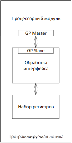
In PIO mode, the processor module operates with programmable logic as a set of registers. To write or read a certain amount of data, you need the constant participation of the processor module. In PIO mode, all transactions are initiated by the processor module. Connecting programmable logic involves using the GP port, where Master is a processor module, Slave is a programmable logic. Project structure when using PIO
2.1 Hardware
- We create a project for Zybo in Vivado, chip type xc7z010clg400-1.
- Create block design. In the Flow Navigator => Create Block Design => the name "ProcessingSystem" => OK.
- Using the "+" button on the field or the Ctrl + I keyboard shortcuts, add the processor core.
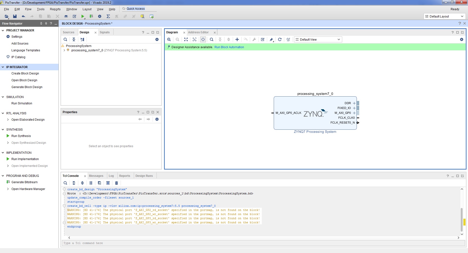
- Let's connect the necessary pins by clicking the Run Block Automation button => OK.
- . Zynq7 Processing System => Import XPS Setting => => OK => OK.
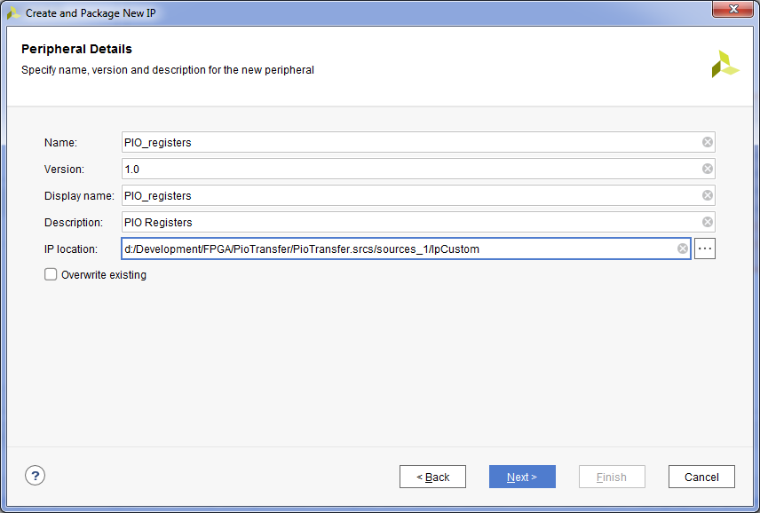
- , . Tools => Create and Package New IP => Next => Create a new AXI4 peripheral => Next => , «PIO_registers» => Next => (4 ), , Lite => Next => Add IP to the repository => Finish.
- , IP . , Flow Navigator => IP Catalog.

- . Ctrl + I => PIO_registers.
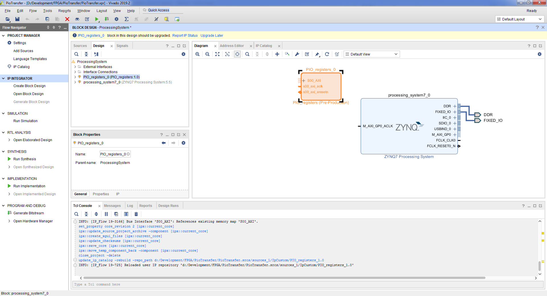
- , . PIO_registers => Edit in IP Packager => OK. Vivado .
- PIO_registers_v1_0.vhd :
iSwitches : in std_logic_vector( 3 downto 0); oLeds : out std_logic_vector( 3 downto 0); ... iSwitches => iSwitches, oLeds => oLeds,
- PIO_registers_v1_0_S_AXI.vhd :
iSwitches : in std_logic_vector( 3 downto 0); oLeds : out std_logic_vector( 3 downto 0);
- :
signal SwitchesReg : std_logic_vector(31 downto 0); ... process (SwitchesReg, slv_reg1, slv_reg2, slv_reg3, axi_araddr, S_AXI_ARESETN, slv_reg_rden) variable loc_addr :std_logic_vector(OPT_MEM_ADDR_BITS downto 0); begin -- Address decoding for reading registers loc_addr := axi_araddr(ADDR_LSB + OPT_MEM_ADDR_BITS downto ADDR_LSB); case loc_addr is when b"00" => reg_data_out <= SwitchesReg; when b"01" => reg_data_out <= slv_reg1; when b"10" => reg_data_out <= slv_reg2; when b"11" => reg_data_out <= slv_reg3; when others => reg_data_out <= (others => '0'); end case; end process; process (S_AXI_ACLK) begin if (rising_edge(S_AXI_ACLK)) then if (S_AXI_ARESETN = '0') then SwitchesReg <= (others => '0'); else SwitchesReg( 3 downto 0) <= iSwitches; end if; end if; end process; process (S_AXI_ACLK) begin if (rising_edge(S_AXI_ACLK)) then if (S_AXI_ARESETN = '0') then oLeds <= (others => '0'); else oLeds <= slv_reg1( 3 downto 0); end if; end if; end process;
- vhd , Package IP – PIO_registers. . Compatibility Life Cycle Production. File Groups => Merge changes from File Group Wizard. Customization Parameters => Merge changes from Customization Parameters Wizard. Review and Package => Re-Package IP => Yes. Vivado .
- Block Design Report IP Status, Upgrade Selected => OK => Skip => OK.
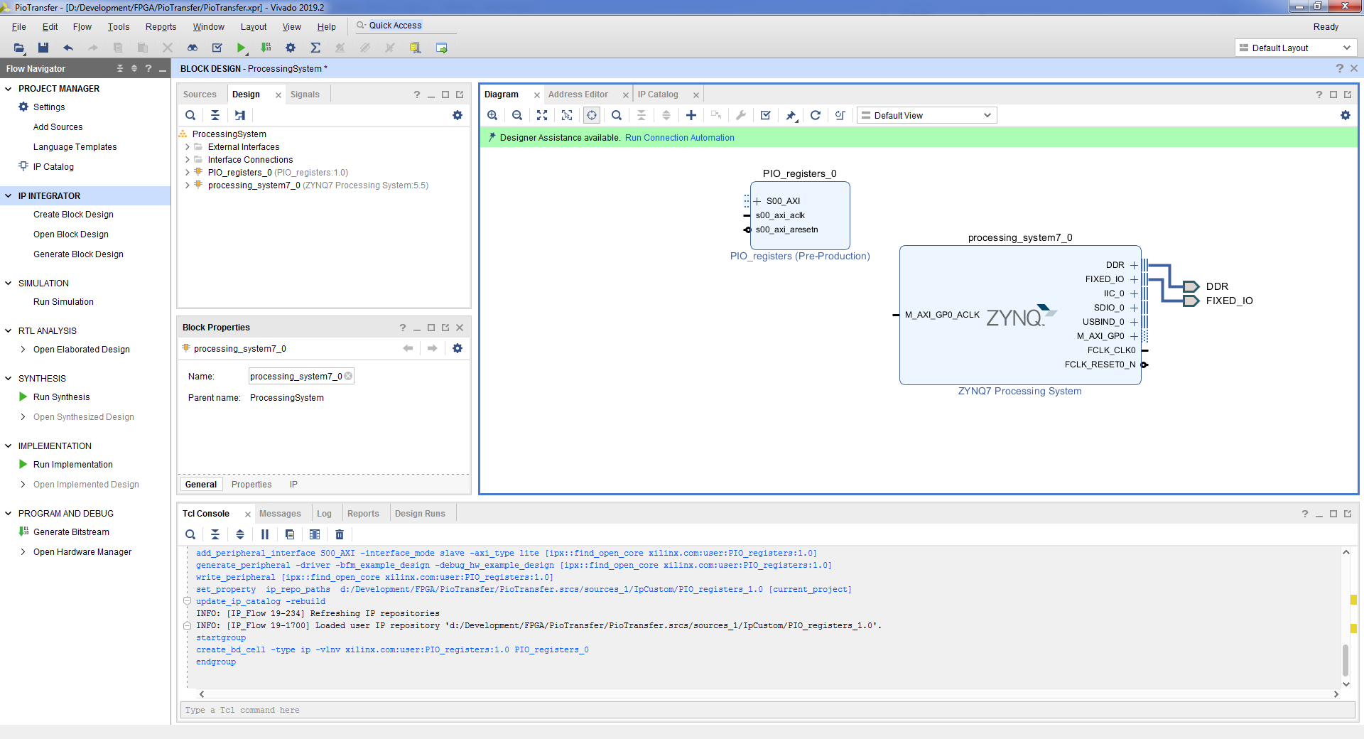
- . Run Connection Automation => OK.

- block design’a. , => Make External.
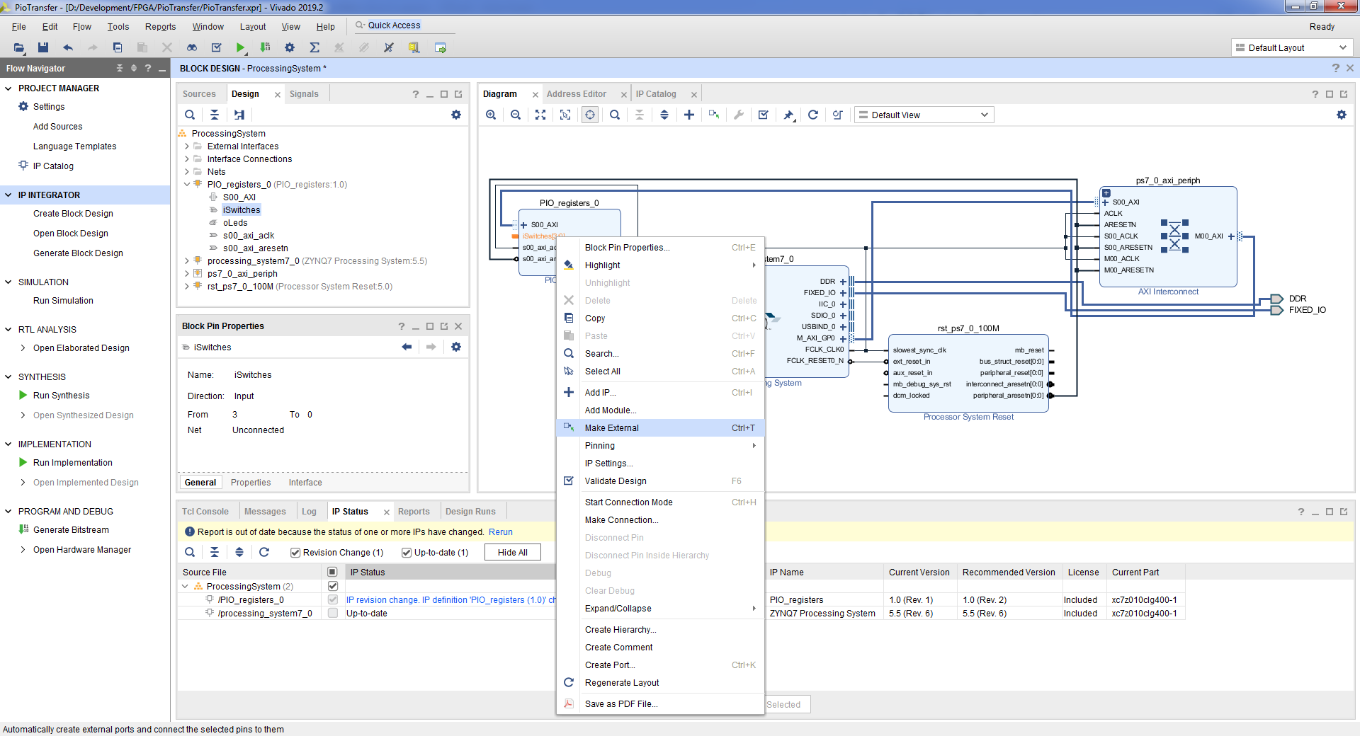
- iSwitches_0 => iSwitches. oLeds_0 => oLeds.
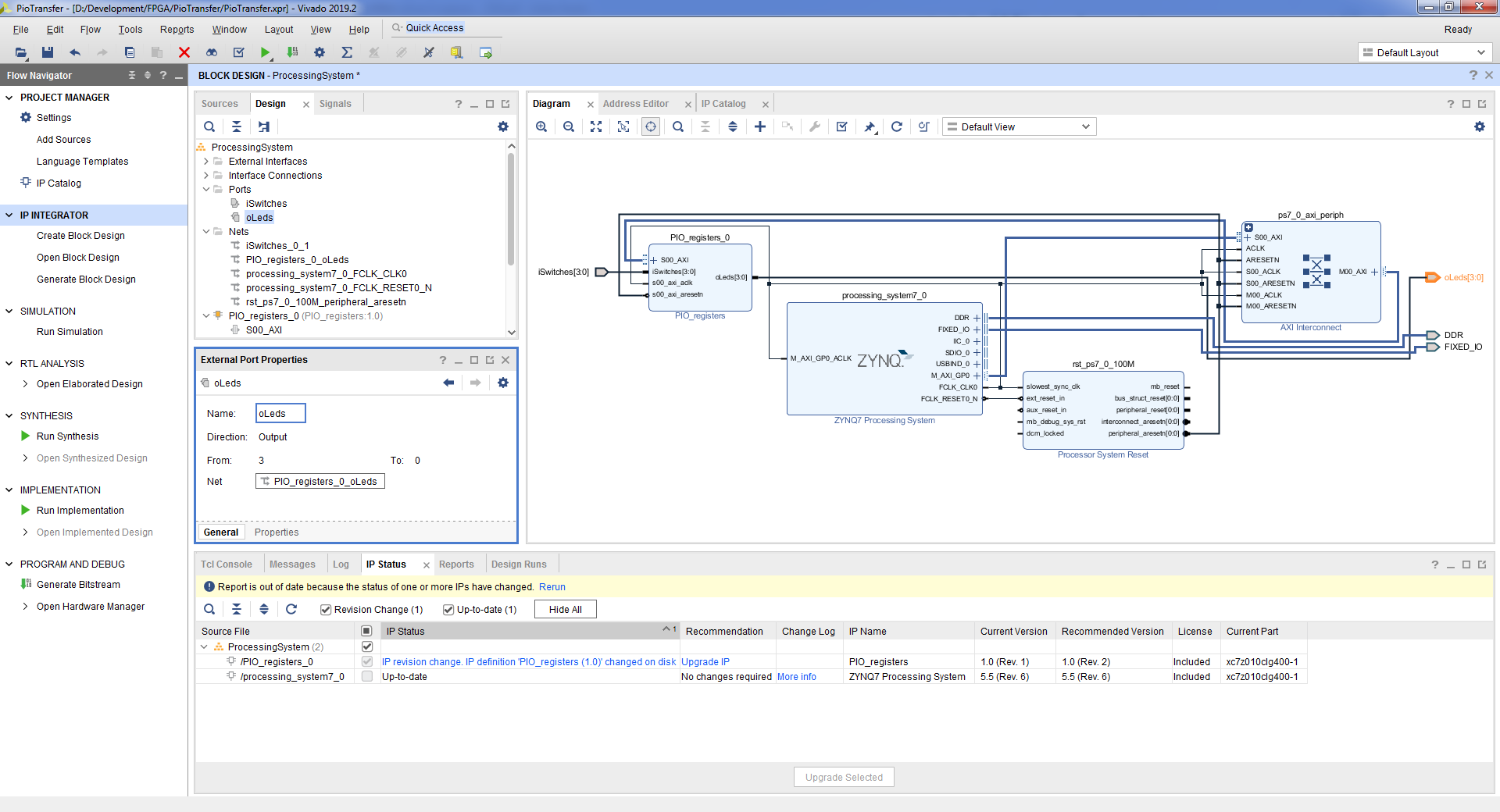
- => Tools => Validate Design => Ok.
- File => Save Block Design.
- block design , Flow Navigator => Project Manager.
- , block design’a. ProcessingSystem.bd, => View Instantiation Template.

- vhd top- block design. File => Add Sources => Add or create design sources => Next => Create File => => OK => Finish => OK => Yes.
- :
entity PioTransfer is port ( DDR_addr : inout std_logic_vector(14 downto 0 ); DDR_ba : inout std_logic_vector( 2 downto 0 ); DDR_cas_n : inout std_logic; DDR_ck_n : inout std_logic; DDR_ck_p : inout std_logic; DDR_cke : inout std_logic; DDR_cs_n : inout std_logic; DDR_dm : inout std_logic_vector( 3 downto 0 ); DDR_dq : inout std_logic_vector(31 downto 0 ); DDR_dqs_n : inout std_logic_vector( 3 downto 0 ); DDR_dqs_p : inout std_logic_vector( 3 downto 0 ); DDR_odt : inout std_logic; DDR_ras_n : inout std_logic; DDR_reset_n : inout std_logic; DDR_we_n : inout std_logic; FIXED_IO_ddr_vrn : inout std_logic; FIXED_IO_ddr_vrp : inout std_logic; FIXED_IO_mio : inout std_logic_vector( 53 downto 0 ); FIXED_IO_ps_clk : inout std_logic; FIXED_IO_ps_porb : inout std_logic; FIXED_IO_ps_srstb : inout std_logic; -- Control iSwitches : in std_logic_vector( 3 downto 0 ); oLeds : out std_logic_vector( 3 downto 0 ) ); end PioTransfer; architecture Behavioral of PioTransfer is begin PS : entity WORK.ProcessingSystem port map ( DDR_addr => DDR_addr, DDR_ba => DDR_ba, DDR_cas_n => DDR_cas_n, DDR_ck_n => DDR_ck_n, DDR_ck_p => DDR_ck_p, DDR_cke => DDR_cke, DDR_cs_n => DDR_cs_n, DDR_dm => DDR_dm, DDR_dq => DDR_dq, DDR_dqs_n => DDR_dqs_n, DDR_dqs_p => DDR_dqs_p, DDR_odt => DDR_odt, DDR_ras_n => DDR_ras_n, DDR_reset_n => DDR_reset_n, DDR_we_n => DDR_we_n, FIXED_IO_ddr_vrn => FIXED_IO_ddr_vrn, FIXED_IO_ddr_vrp => FIXED_IO_ddr_vrp, FIXED_IO_mio => FIXED_IO_mio, FIXED_IO_ps_clk => FIXED_IO_ps_clk, FIXED_IO_ps_porb => FIXED_IO_ps_porb, FIXED_IO_ps_srstb => FIXED_IO_ps_srstb, -- Control iSwitches => iSwitches, oLeds => oLeds ); end Behavioral;
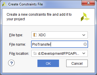
- . File => Add sources => Add or create constrains => Next => Create File => => OK => Finish.
- :
#Switches set_property PACKAGE_PIN G15 [get_ports {iSwitches[0]}] set_property PACKAGE_PIN P15 [get_ports {iSwitches[1]}] set_property PACKAGE_PIN W13 [get_ports {iSwitches[2]}] set_property PACKAGE_PIN T16 [get_ports {iSwitches[3]}] set_property IOSTANDARD LVCMOS33 [get_ports {iSwitches[*]}] #LEDs #IO_L23P_T3_35 set_property PACKAGE_PIN M14 [get_ports {oLeds[0]}] set_property PACKAGE_PIN M15 [get_ports {oLeds[1]}] set_property PACKAGE_PIN G14 [get_ports {oLeds[2]}] set_property PACKAGE_PIN D18 [get_ports {oLeds[3]}] set_property IOSTANDARD LVCMOS33 [get_ports {oLeds[*]}]
- . Flow Navigator => Generate Bitstream => OK. , , .
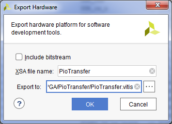
- . File => Export => Export Hardware => => OK. .xsa
2.2
Now you need to write an application that runs on the processor module that will read data from the programmable logic and write data to the programmable logic. You need to start the Vitis development environment and create an application using the Hello World template, an example of this is shown in the previous article [1].
The address of the created kernel for access from the processor module can be viewed in Vivado. In Flow Navigator => Open Block Design => Address Editor Tab. In this case, the address is 0x43C0_0000. A register is located at this address, in which the attribute is stored, in what state the switches are. Accordingly, at the address 0x43C0_0004 there is a register that is connected to the LEDs.
In Vitis, open the helloworld.c file and fill in:
int main()
{
init_platform();
u32 Status = 0x00;
u32 Command = 0x00;
xil_printf("Hello World\n\r");
while (1)
{
Status = Xil_In32(0x43C00000);
xil_printf("Status %x\n\r", Status);
if (Status == 0x01 || Status == 0x02 || Status == 0x04 || Status == 0x08)
{
Command = 0x01;
}
else if (Status == 0x03 || Status == 0x5 || Status == 0x06 || Status == 0x9 || Status == 0xA || Status == 0x0C)
{
Command = 0x03;
}
else if (Status == 0x7 || Status == 0x0B || Status == 0x0D || Status == 0x0E)
{
Command = 0x7;
}
else if (Status == 0x0F)
{
Command = 0x0F;
}
else
{
Command = 0x00;
}
xil_printf("Command %x\n\r", Command);
Xil_Out32(0x43C00004, Command);
usleep(1000000);
}
cleanup_platform();
return 0;
}
Where the Xil_In32 function is used to read 4 bytes of data from the programmable logic, and Xil_Out32, respectively, to write 4 bytes of data to the programmable logic.
2.3 Results
We assemble the application, create a firmware file and upload it to the board. Described in the previous article [1].
Launch, look in the com-port monitor:
Xilinx First Stage Boot Loader Release 2019.2 Dec 9 2020-15:16:52 Silicon Version 3.1 Boot mode is QSPI SUCCESSFUL_HANDOFF FSBL Status = 0x1 Hello World Status 0 Command 0 Status 8 Command 1 Status C Command 3 Status D Command 7 Status F Command F
Everything works correctly.
Thus, to access the programmable logic in PIO mode, it is necessary to implement one of the communication interfaces with the processor module in the programmable logic, where the processor module is the initiator. This interface is represented only by the GP port.
Let's see how quickly requests to programmable logic are processed through the GP port. To do this, in an application running on a processor module, add several entries in a row to a register in programmable logic, and measure the time between transactions in programmable logic using the bus signals pulled into the debugger.
When the Axi-Lite bus is operating at 100 MHz, there is an average of 23 clock cycles between requests. Let's change the bus frequency to 200 MHz. The pause between requests becomes 33 cycles on average.
In total, 4 bytes of data are transmitted at 100 MHz for 23 clocks. The speed is: 32 / (23 * 10ns) = 139 130 434 bps ≈ 135 869 kbps ≈ 132 Mbps ≈ 16 MB / s.
In total, 4 bytes of data are transmitted at 200 MHz for 33 clocks. The speed is 32 / (33 * 5ns) = 193 939 393 bps ≈ 189 393 Kbps ≈ 184 Mbps ≈ 23 Mbps.
Thus, you can achieve a speed of 23 MB / s, but with the constant participation of the processor module.
Project: github.com/Finnetrib/PioTransfer
3 Data transfer in DMA mode
Data transfer in DMA mode implies that the processor module configures the data exchange parameters and does not participate directly in the exchange. Thus, two goals are achieved: reducing the load on the processor module and increasing the data processing speed. The price for this is the complication of the hardware.
In Zynq, it is possible to use several ip-cores that implement DMA functions. This article will look at the core AXI DMA [2].
AXI DMA has two channels MM2S and S2MM. Channel MM2S (Memory-mapped to stream) is used to transfer data from the processor module to the programmable logic. The S2MM (Stream to memory-mapped) channel is used to transfer data from the programmable logic to the processor module. The channels work independently of each other.
AXI DMA has two use cases:
- Direct Register Mode
- Scatter / Gather Mode
Direct Register Mode uses one set of registers, which allows one buffer to be transferred from the programmable logic to the processor module and vice versa. For example, to transfer a data buffer from programmable logic to a processor module, you need to fill in the address and buffer size fields and start DMA. As a result, DMA will fill one buffer in the processor unit and stop.
Scatter / Gather Mode uses a list of descriptors. DMA processes the buffer described in the descriptor and proceeds to processing the buffer described in the next descriptor.
3.1 Hardware

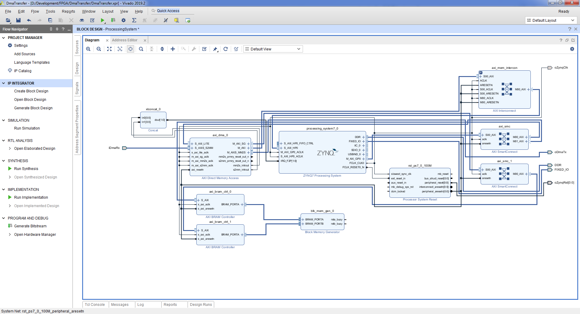
Project structure when using DMA
Let's consider the option when the list of descriptors is stored in programmable logic. The DMA block has a control port that connects to the GP port of the processor unit. There is also an HP port used to access the processor RAM. The descriptor list is stored in the descriptor memory. The descriptor memory can be accessed from both the DMA and the processor unit. The processor module fills in the descriptors, the DMA reads out the descriptors.
- Create block design. In the Flow Navigator => Create Block Design => the name "ProcessingSystem" => OK.
- Using the "+" button on the field or the Ctrl + I keyboard shortcuts, add the processor core.
- Let's connect the necessary pins by clicking the Run Block Automation button => OK.
- . Zynq7 Processing System => Import XPS Setting => => OK => OK
- AXI Direct Memory Access, AXI BRAM Controller, Block Memory Generator.
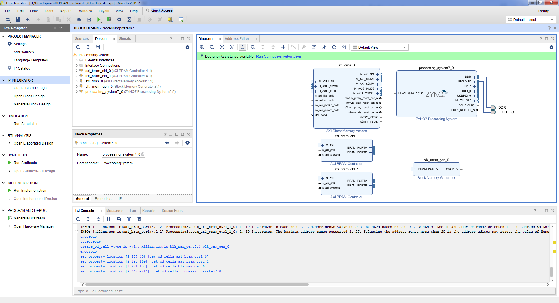
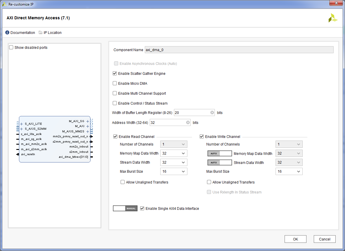
- AXI Direct Memory Access, . «Enable Scatter Gather Engine» , . «Enable Control / Status Stream» AXI Ethernet, . «With of Buffer Length Register» , . 20, 2^20 = 1 048 576 . «Address With» . 32 . «Enable Read Channel» «Enable Write Channel» . «Enable Single AXI4 Data interface» , . «OK» .
- AXI BRAM Controller. «Number of BRAM Interfaces» 1. «OK» .
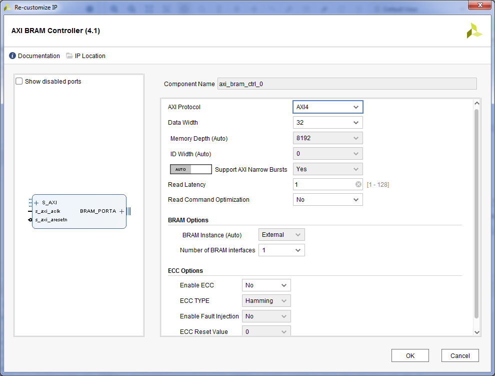
- AXI BRAM Controller.
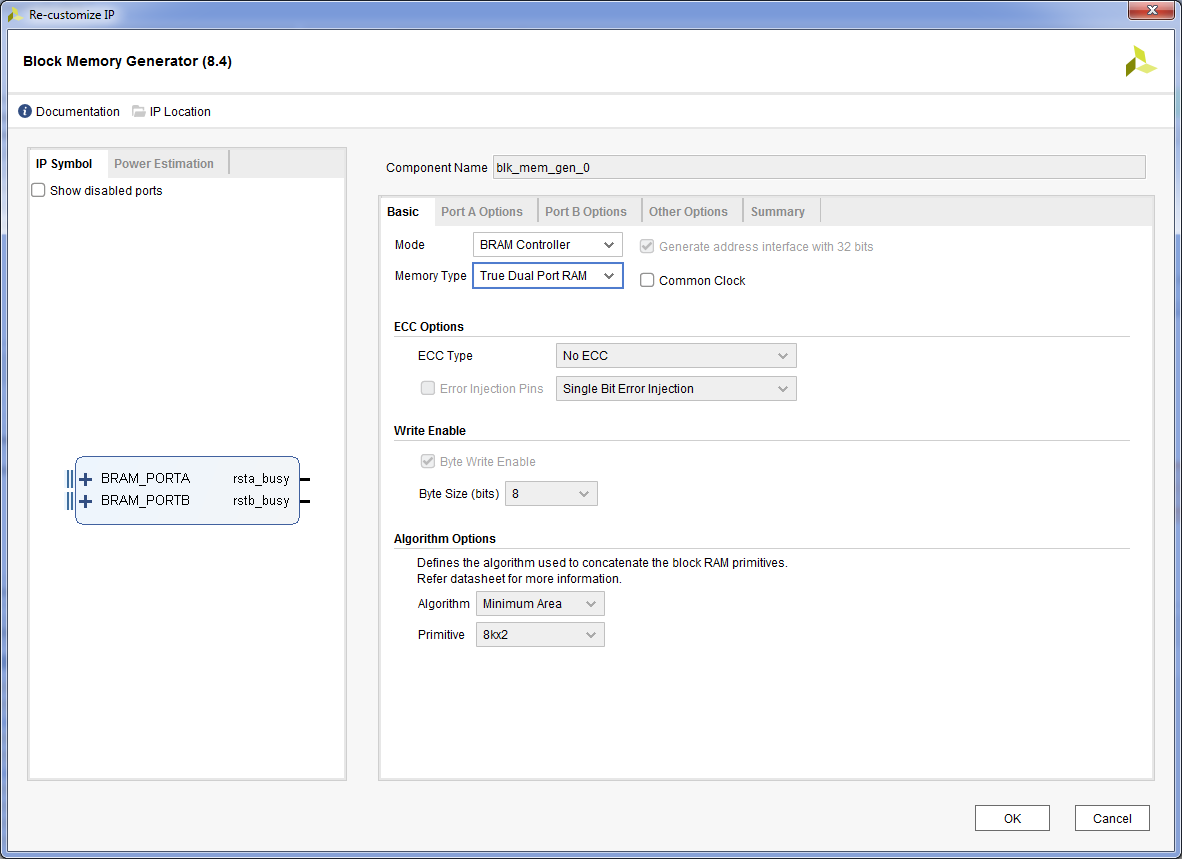
- Block Memory Generator. «Memory Type» «True Dual Port RAM». «OK» .
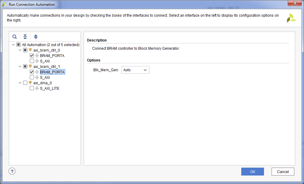
- . «Run Connection Automation» => axi_bram_ctrl_0 BRAM_PORTA => axi_bram_ctrl_1 BRAM_PORTA => OK.
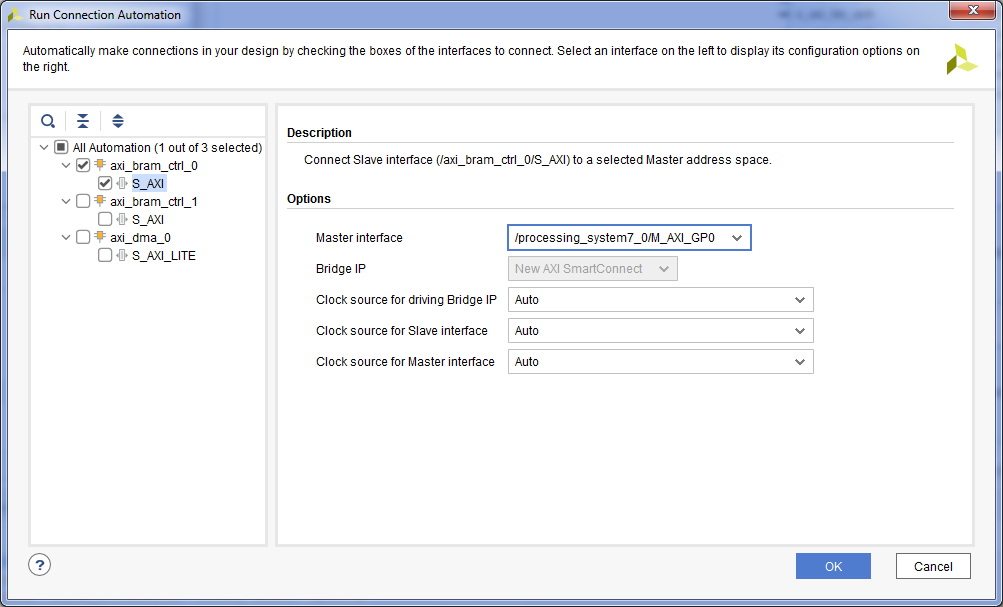
- . «Run Connection Automation» => axi_bram_ctrl_0 S_AXI => Master Interface /processing_system7_0/M_AXI_GP0 => OK. , .
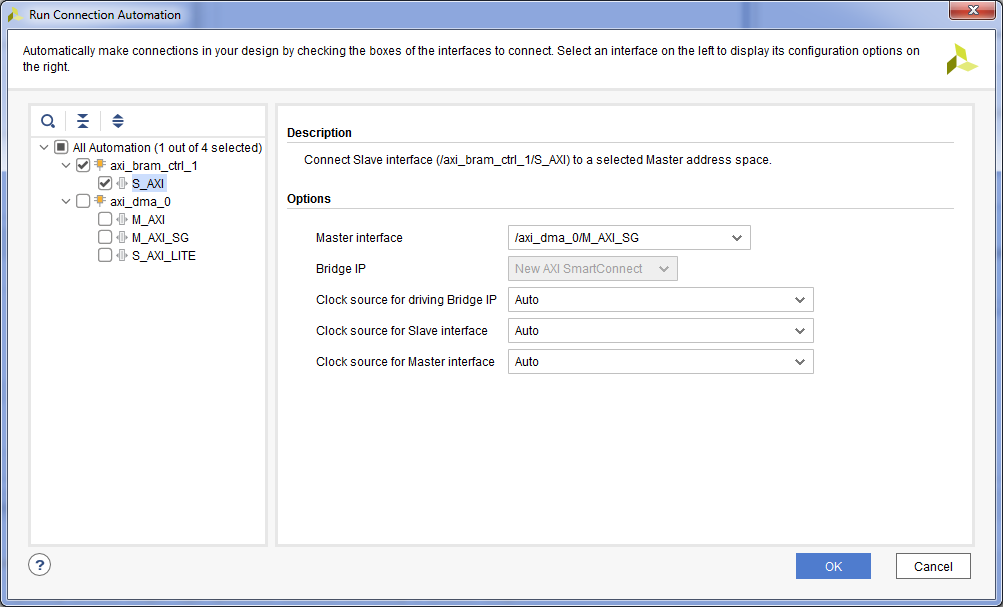
- DMA. «Run Connection Automation» => axi_bram_ctrl_1 S_AXI => Master Interface /axi_dma_0/M_AXI_SG => OK. , DMA .
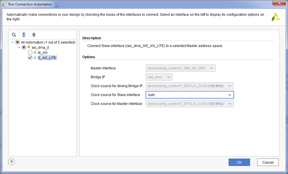
- DMA . «Run Connection Automation» => axi_dma_0 S_AXI_LITE => OK.
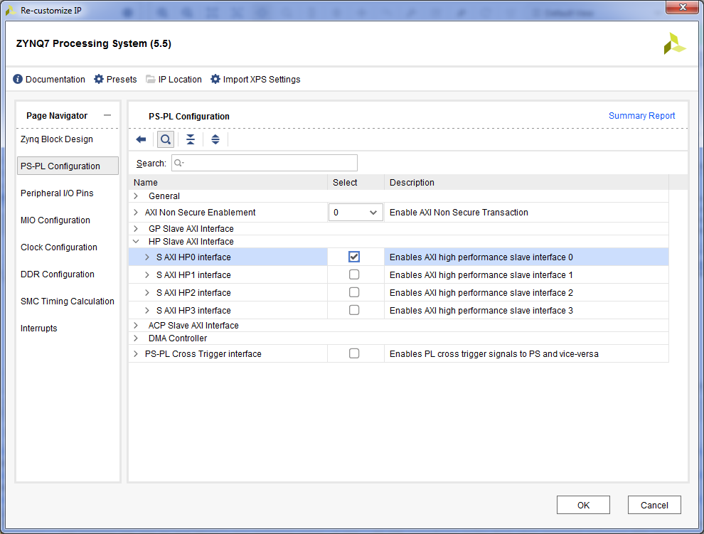
- – HP . Zynq7 Processing System => PS-PL Configuration => HP Slave AXI Interface => S AXI HP0 Interface.
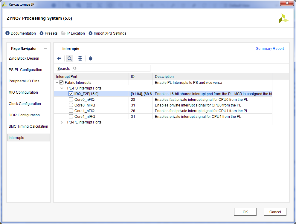
Interrupts => Fabric Interrupts => PL-PS Interrupts Ports => Fabric Interrupts => IRQ_F2P => OK.
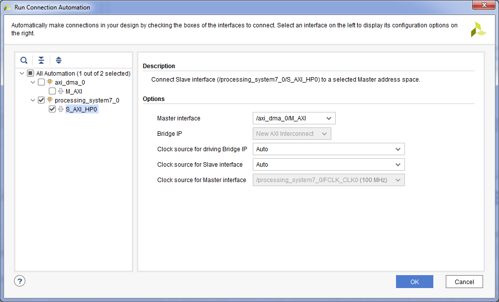
- DMA . «Run Connection Automation» => processing_system7_0 S_AXI_HP0 => Master Interface /axi_dma_0/M_AXI => OK.
- DMA . Concat + Ctrl + I.
- mm2s_introut DMA, . mm2s_introut In0 Concat. , , .
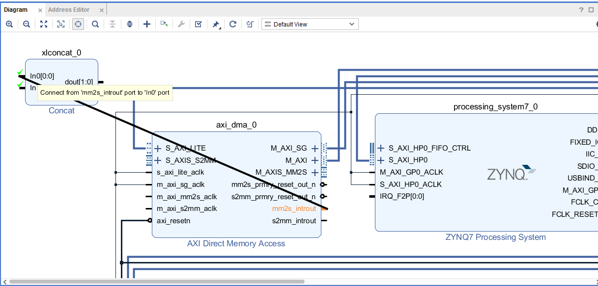
- s2mm_introut, In1 Concat.
- dout Concat IRQ_F2P Zynq7 Processing System.
- DMA . DMA . Block Design, . Create Port Ctrl + K. , => OK.
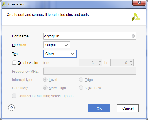
- FCLK_CLK0 Zynq7 Processing System.
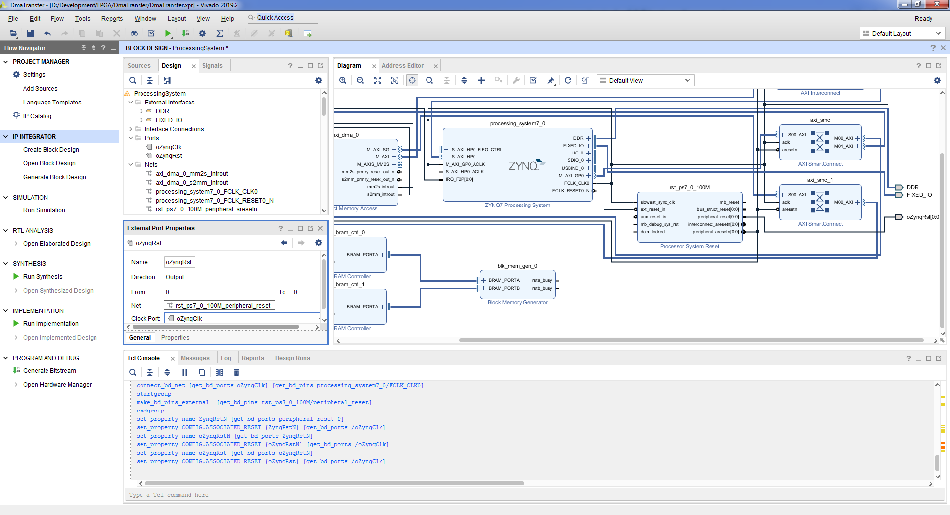
- . peripheral_reset Processor System Reset => => Make External.
- , , .
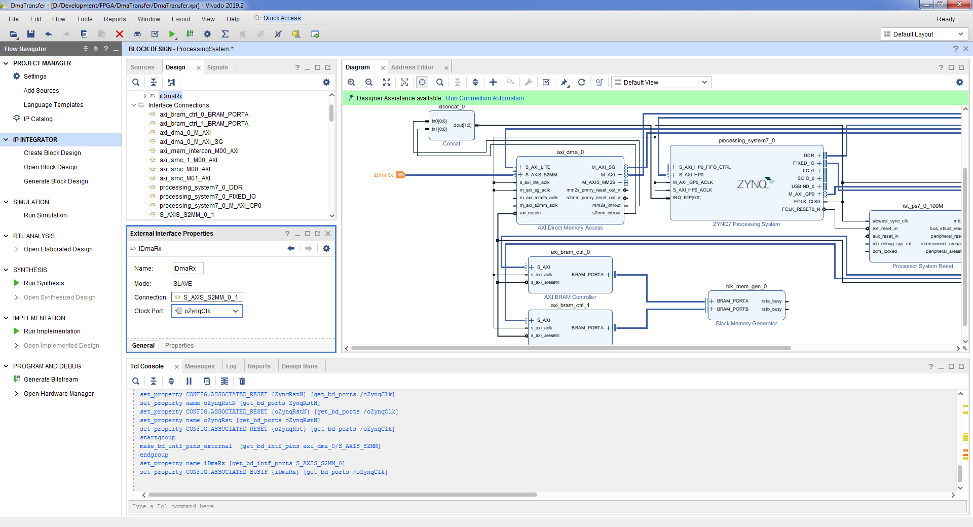
- DMA. S_AXIS_S2MM AXI Direct Memory Access => => Make External.
- , , .
- DMA. M_AXIS_MM2S AXI Direct Memory Access => => Make External.
- , , .

- S_AXIS_S2MM M_AXIS_MM2S AXI Direct Memory Access. «Run Connection Automation» => m_axi_mm2s_aclk m_axi_s2mm_aclk => OK
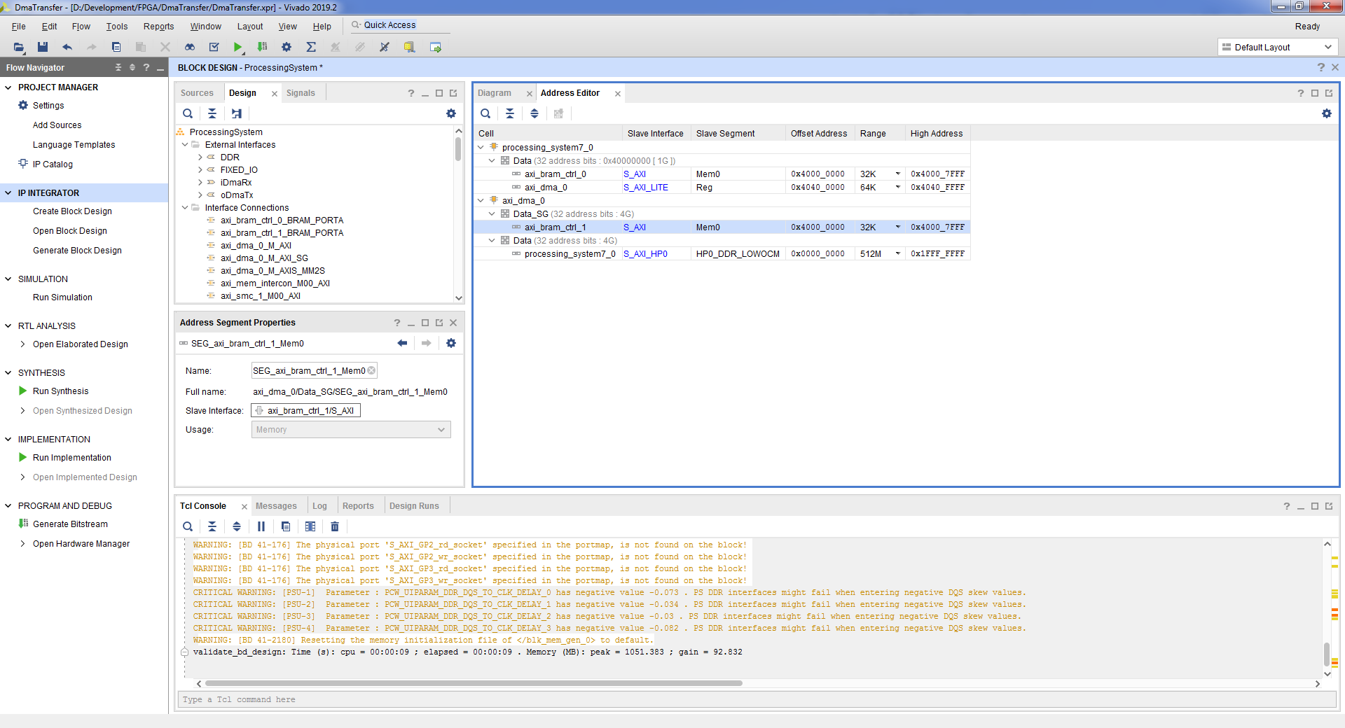
- , DMA . . Address Editor => processing_system7_0 / Data / axi_bram_ctrl_0 => Offset Address 0x4000_0000 => Range 32K. axi_dma_0 / Data_SG / axi_bram_ctrl_1 => Offset Address 0x4000_0000 => Range 32K.
- Tools => Validate Design => OK. :
- File => Save Block Design.
- block design , Flow Navigator => Project Manager.
- , block design’a. ProcessingSystem.bd, => View Instantiation Template.
- vhd top- block design. File => Add Sources => Add or create design sources => Next => Create File => => OK => Finish => OK => Yes.

- :
entity DmaTransfer is port ( DDR_addr : inout std_logic_vector(14 downto 0); DDR_ba : inout std_logic_vector( 2 downto 0); DDR_cas_n : inout std_logic; DDR_ck_n : inout std_logic; DDR_ck_p : inout std_logic; DDR_cke : inout std_logic; DDR_cs_n : inout std_logic; DDR_dm : inout std_logic_vector( 3 downto 0); DDR_dq : inout std_logic_vector(31 downto 0); DDR_dqs_n : inout std_logic_vector( 3 downto 0); DDR_dqs_p : inout std_logic_vector( 3 downto 0); DDR_odt : inout std_logic; DDR_ras_n : inout std_logic; DDR_reset_n : inout std_logic; DDR_we_n : inout std_logic; FIXED_IO_ddr_vrn : inout std_logic; FIXED_IO_ddr_vrp : inout std_logic; FIXED_IO_mio : inout std_logic_vector(53 downto 0); FIXED_IO_ps_clk : inout std_logic; FIXED_IO_ps_porb : inout std_logic; FIXED_IO_ps_srstb : inout std_logic ); end DmaTransfer; architecture Behavioral of DmaTransfer is signal RxData : std_logic_vector(31 downto 0); signal RxKeep : std_logic_vector( 3 downto 0); signal RxLast : std_logic; signal RxValid : std_logic; signal RxReady : std_logic; signal TxData : std_logic_vector(31 downto 0); signal TxKeep : std_logic_vector( 3 downto 0); signal TxLast : std_logic; signal TxValid : std_logic; signal TxReady : std_logic; signal clk : std_logic; signal rst : std_logic; signal FifoDataW : std_logic_vector(36 downto 0); signal FifoWrite : std_logic; signal FifoRead : std_logic; signal FifoDataR : std_logic_vector(36 downto 0); signal FifoEmpty : std_logic; signal FifoFull : std_logic; begin PS : entity WORK.ProcessingSystem port map ( DDR_addr => DDR_addr, DDR_ba => DDR_ba, DDR_cas_n => DDR_cas_n, DDR_ck_n => DDR_ck_n, DDR_ck_p => DDR_ck_p, DDR_cke => DDR_cke, DDR_cs_n => DDR_cs_n, DDR_dm => DDR_dm, DDR_dq => DDR_dq, DDR_dqs_n => DDR_dqs_n, DDR_dqs_p => DDR_dqs_p, DDR_odt => DDR_odt, DDR_ras_n => DDR_ras_n, DDR_reset_n => DDR_reset_n, DDR_we_n => DDR_we_n, FIXED_IO_ddr_vrn => FIXED_IO_ddr_vrn, FIXED_IO_ddr_vrp => FIXED_IO_ddr_vrp, FIXED_IO_mio => FIXED_IO_mio, FIXED_IO_ps_clk => FIXED_IO_ps_clk, FIXED_IO_ps_porb => FIXED_IO_ps_porb, FIXED_IO_ps_srstb => FIXED_IO_ps_srstb, -- Dma Channel iDmaRx_tdata => RxData, iDmaRx_tkeep => RxKeep, iDmaRx_tlast => RxLast, iDmaRx_tready => RxReady, iDmaRx_tvalid => RxValid, oDmaTx_tdata => TxData, oDmaTx_tkeep => TxKeep, oDmaTx_tlast => TxLast, oDmaTx_tready => TxReady, oDmaTx_tvalid => TxValid, -- System oZynqClk => clk, oZynqRst(0) => rst ); FifoDataW(31 downto 0) <= not TxData; FifoDataW(35 downto 32) <= TxKeep; FifoDataW( 36) <= TxLast; FifoWrite <= TxValid and not FifoFull; TxReady <= not FifoFull; EchFifo : entity WORK.SyncFifoBram37x1024 port map ( clk => clk, srst => rst, din => FifoDataW, wr_en => FifoWrite, rd_en => FifoRead, dout => FifoDataR, full => open, empty => FifoEmpty, prog_full => FifoFull ); RxData <= FifoDataR(31 downto 0); RxKeep <= FifoDataR(35 downto 32); RxLast <= FifoDataR(36); RxValid <= not FifoEmpty; FifoRead <= RxReady; end Behavioral;
- . Flow Navigator => Generate Bitstream => OK. , , .
- . File => Export => Export Hardware => => OK. .xsa

3.2
Now you need to write an application that runs on the processor module. You need to start the Vitis development environment and create an application using the Hello World template, an example of this is shown in the previous article.
The format of the descriptors for Axi DMA is described in the kernel document [2]. The descriptor is 52 bytes in size, however, the address at which the descriptor is located must be 64 bytes aligned.
Briefly about the format of the descriptor:
- NXTDESC - address of the next descriptor;
- NXTDESC_MSB - high 32 bits of the next descriptor address;
- BUFFER_ADDRESS - buffer address;
- BUFFER_ADDRESS_MSB - high 32 bits of the buffer address;
- RESERVED - not used;
- RESERVED - not used;
- CONTROL - sets the buffer size, signs of the beginning and end of the packet;
- STATUS - shows how many bytes were received / transmitted, processed / not processed;
- APP0 - used to work with the "Control / Status Stream" channel;
- APP1 - used to work with the Control / Status Stream channel;
- APP2 - used to work with the Control / Status Stream channel;
- APP3 - used to work with the "Control / Status Stream" channel;
- APP4 - used to work with the "Control / Status Stream" channel.
Addresses in programmable logic for access from the processor module can be viewed in Vivado. In Flow Navigator => Open Block Design => Address Editor Tab. In this case, the DMA address is 0x4040_0000. The address of the beginning of the memory area for descriptors is 0x4000_0000.
- In Vitis, open the helloworld.c file and include the following libraries
#include <xil_io.h> #include "sleep.h" #include "xil_cache.h" #include "xil_mem.h"
- , 64 . , 32 32 768 / 64 = 512 . 256 256 .
#define DESC_COUNT 256 ... /** Descriptors for receive */ struct SGDesc RxDesc[DESC_COUNT]; /** Descriptors for transmit */ struct SGDesc TxDesc[DESC_COUNT];
- , , .
/** Flush Cache */ Xil_DCacheFlush(); /** Disable Cache */ Xil_DCacheDisable();
- , .
for (u16 desc = 0; desc < DESC_COUNT; desc++) { for (u32 i = 0; i < BUFFER_SIZE; i++) { TxBuffer[desc][i] = desc + i; } }
- .
for (u16 i = 0; i < DESC_COUNT; i++) { TxDesc[i].NXTDESC = &TxDesc[i]; TxDesc[i].NXTDESC_MSB = 0x0; TxDesc[i].BUFFER_ADDRESS = &TxBuffer[i][0]; TxDesc[i].BUFFER_ADDRESS_MSB = 0x0; TxDesc[i].RESERVED0 = 0x0; TxDesc[i].RESERVED1 = 0x0; TxDesc[i].CONTROL = 0xC000000 + sizeof(TxBuffer[i]); TxDesc[i].STATUS = 0x0; TxDesc[i].APP0 = 0x0; TxDesc[i].APP1 = 0x0; TxDesc[i].APP2 = 0x0; TxDesc[i].APP3 = 0x0; TxDesc[i].APP4 = 0x0; }
- , .
DescAddr = 0x40000000; for (u16 i = 0; i < DESC_COUNT; i++) { Xil_MemCpy(DescAddr, &TxDesc[i], sizeof(TxDesc[i])); DescAddr += 0x40; }
- .
/** Write pointer to next pointer */ DescAddr = 0x40000000; for (u16 i = 0; i < DESC_COUNT - 1; i++) { Xil_Out32(DescAddr, DescAddr + 0x40); DescAddr += 0x40; } /** Write pointer for last descriptor */ Xil_Out32(DescAddr, DescAddr);
- .
/** Fill descriptor to receive */ for (u16 i = 0; i < DESC_COUNT; i++) { RxDesc[i].NXTDESC = &RxDesc[i]; RxDesc[i].NXTDESC_MSB = 0x0; RxDesc[i].BUFFER_ADDRESS = &RxBuffer[i][0]; RxDesc[i].BUFFER_ADDRESS_MSB = 0x0; RxDesc[i].RESERVED0 = 0x0; RxDesc[i].RESERVED1 = 0x0; RxDesc[i].CONTROL = sizeof(RxBuffer[i]); RxDesc[i].STATUS = 0x0; RxDesc[i].APP0 = 0x0; RxDesc[i].APP1 = 0x0; RxDesc[i].APP2 = 0x0; RxDesc[i].APP3 = 0x0; RxDesc[i].APP4 = 0x0; } /** Copy receive descriptor for memory of descriptors */ DescAddr = 0x40000000 + 0x4000; for (u16 i = 0; i < DESC_COUNT; i++) { Xil_MemCpy(DescAddr, &RxDesc[i], sizeof(RxDesc[i])); DescAddr += 0x40; } /** Write pointer to next pointer */ DescAddr = 0x40000000 + 0x4000; for (u16 i = 0; i < DESC_COUNT - 1; i++) { Xil_Out32(DescAddr, DescAddr + 0x40); DescAddr += 0x40; } /** Write pointer for last descriptor */ Xil_Out32(DescAddr, DescAddr);
- DMA . DMA .
/** Reset DMA and setup */ /** MM2S */ Xil_Out32(0x40400000, 0x0001dfe6); Xil_Out32(0x40400000, 0x0001dfe2); /** S2MM */ Xil_Out32(0x40400030, 0x0001dfe6); Xil_Out32(0x40400030, 0x0001dfe2); /** PL => PS */ Xil_Out32(0x4040003c, 0x00000000); Xil_Out32(0x40400038, 0x40004000); Xil_Out32(0x40400030, 0x0001dfe3); Xil_Out32(0x40400044, 0x00000000); Xil_Out32(0x40400040, 0x40007FC0); /** PS => PL */ Xil_Out32(0x4040000C, 0x00000000); Xil_Out32(0x40400008, 0x40000000); Xil_Out32(0x40400000, 0x0001dfe3); Xil_Out32(0x40400014, 0x00000000); Xil_Out32(0x40400010, 0x40003FC0);
- , . , , .
/** Wait ready in last descriptor */ while (1) { status = Xil_In32(0x40003FDC); if ((status & 0x80000000) == 0x80000000) { break; } else { countWait++; usleep(100); } } xil_printf("Time %x \n\r", countWait);
3.3
We assemble the application, create a firmware file and upload it to the board. Described in the previous article [1].
Launch, look in the com-port monitor:
Xilinx First Stage Boot Loader Release 2019.2 Dec 16 2020-15:11:44 Silicon Version 3.1 Boot mode is QSPI SUCCESSFUL_HANDOFF FSBL Status = 0x1 Hello World Time 10F
Thus, for data exchange between the processor module and the programmable logic, one of the communication interfaces with the processor module must be implemented in the programmable logic, where the initiator is the programmable logic. Such interfaces are represented by ports GP, HP, ACP. In the previous article [1] they were all considered.
Let's calculate the data transfer rate: (256 times * 102400 bytes) / (271 * 100 μs) ≈ 967 321 033 bytes / s ≈ 944 649 KB / s ≈ 922 MB / s.
Bit rate 7,738,568,264 bps.
The theoretical speed is 32 bits * 250 MHz = 8,000,000,000 bits / s.
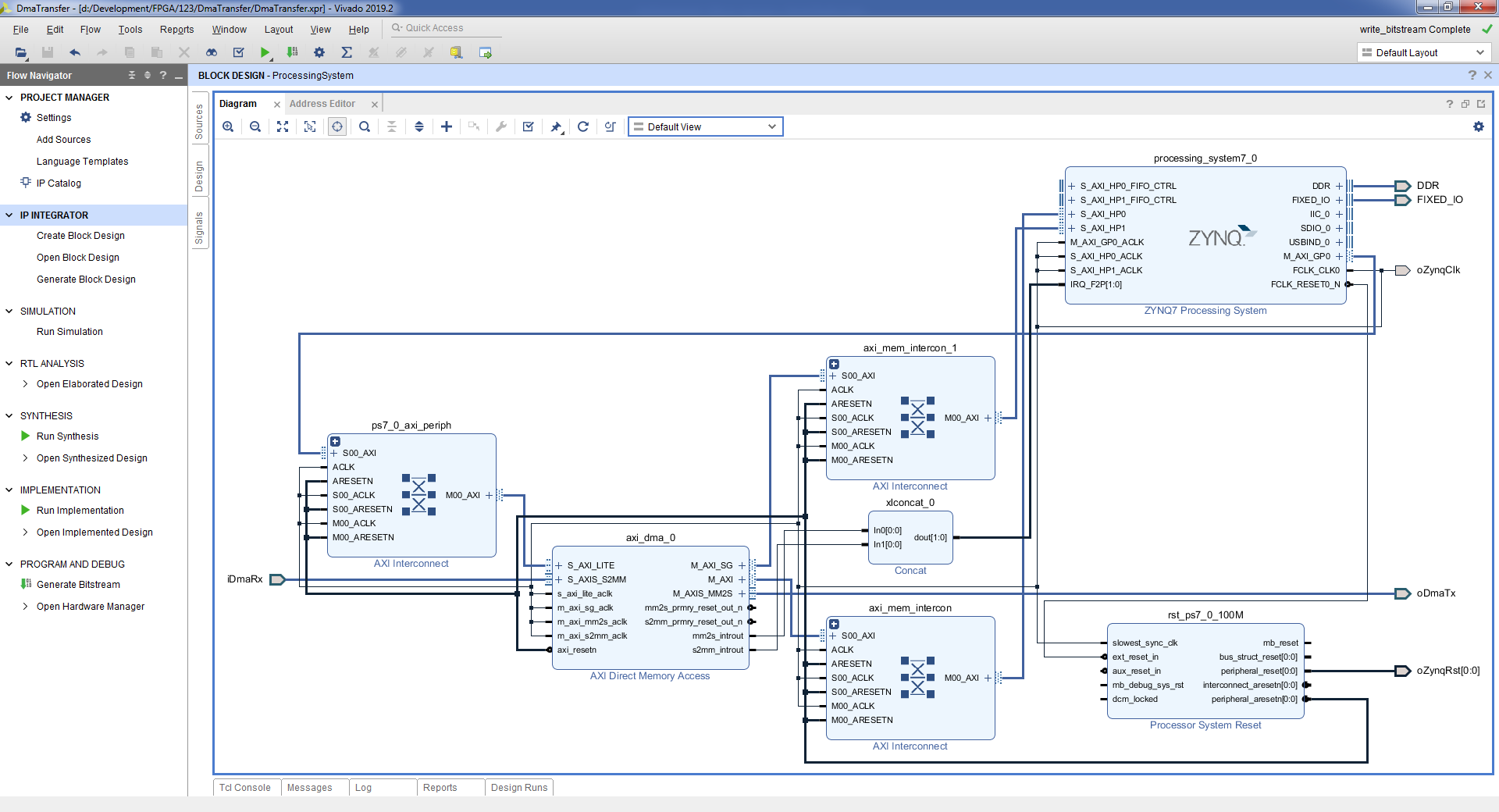
Also, it is possible to store descriptors not in the programmable logic memory, but in the random access memory connected to the processor module. In this case, the M_AXI_SG port connects to the HP Zynq port.
Let's consider the first option, when different HP ports are used for DMA access to data and to descriptors in the processor's RAM. Let's modify the firmware in the programmable logic so that we get the following scheme: Access to data and descriptors through different ports We will not provide the source code of the application. The only difference is that the descriptors do not need to be copied into the programmable logic memory. However, it is necessary to take into account the condition that the address of each descriptor is 64-byte aligned.
After launching the application, we will see in the com-port monitor that the execution time for copying the data buffer has not changed, also 271 * 100 μs.
Let us consider the second option, when the same port is used to access DMA and descriptors in the processor's RAM. Let's modify the firmware in the programmable logic to get the following scheme: Access to data and descriptors through the same port The source code of the application has not changed from the previous version. After starting the application, in the monitor of the com-port we will see the new execution time of the buffer copying operation: 398 * 100 μs.

As a result, the processing speed will be: (256 times * 102400 bytes) / (398 * 100 μs) ≈ 658 653 266 bytes / s ≈ 643 216 KB / s ≈ 628 MB / s.
Bit rate 5 269 226 128 bps.
Project: github.com/Finnetrib/DmaTransfer
4 Conclusion
In this article, we looked at two implementations of data exchange between the processor module and programmable logic. The PIO mode is easy to implement and allows you to get a speed of up to 23 MB / s, the DMA mode is somewhat more complicated, but the speed is also higher - up to 628 MB / s.