
The simplest accelerometer, how does it work?
An accelerometer is a device that measures the projection of the apparent acceleration (the difference between the object's true acceleration and gravitational acceleration). How it works can be explained using a simple model.
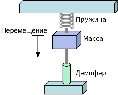
Mechanical accelerometer device model ( original )
When acceleration increases, the mass will stretch the spring. According to Hooke's law from the school physics curriculum, you can easily find the acceleration of the system:
, where k is the coefficient of elasticity of the spring, Is its tension and m is the mass of the load.
Using three perpendicularly located sensors, it is possible to find out the acceleration of an object along 3 axes, and knowing the initial conditions, determine the position of the body in space.
This uncomplicated model is the basis for the operation of most accelerometers, which can be divided into 3 main subgroups:
- mechanical
- electronic
- piezoelectric
There are also thermal and optical ones, but we will not consider them. If everything is clear with mechanical ones (in fact, their work is reflected by the model from above), then with electronic and piezoelectric ones it is a little more interesting.
Piezoelectric accelerometer
This type of sensors is based on the piezo effect, which was discovered in 1954 by Smith in semiconductors such as germanium and silicon. This discovery gave a strong impetus to the development of sensors and generators. The effect is the generation of stress by the piezoelectric element upon deformation.

Animation of the piezoelectric effect ( original )
With increasing acceleration, the inert mass increases / decreases the pressure on the piezoelectric element. Thanks to the piezoelectric effect, a signal is generated that depends on the external acceleration.

Piezoelectric accelerometer device ( original )
Sensors of this type require an additional amplifier, which increases the signal amplitude, and creates a low impedance output to work with external devices. The Preload Bolt is used to calibrate the acceleration zero value, the mass of which is calculated to correspond to the acceleration zero point in the system.
Sensors of this type are still very common, and are mainly used in systems requiring high reliability - automotive. For commercial electronics, electronic accelerometers are often used, which are smaller and cheaper.
Electronic accelerometers
The principle of operation of electronic sensors is based on a change in the capacitance of capacitors with a change in acceleration. The simplest model of work is shown in the picture.
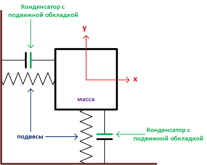
The device of a 2-axis electro-mechanical accelerometer
When the acceleration changes, the mass changes the distance between the capacitor plates. From the simplest formula for the capacitance of a condenser it follows that when d changes in the distance between the plates, the capacitance of the capacitor will also change. This method is widely used due to the development of MEMS (MEMS) - microelectromechanical systems.
MEMS technologies make it possible to create capacitors with movable plates on a silicon substrate, which significantly reduces the size of the device, and, which is not unimportant, its cost.

The device of a 2-axis electro-mechanical accelerometer (original from the book "Introductory MEMS" . Further illustrations are also taken from this book)
The reader probably has a question: "how exactly to detect a change in capacitor capacitance?" I will try to give an exhaustive answer to this question.
MEMS accelerometer device. How to turn a change in capacitance into a signal?
Capacitive half-bridge
So, before describing the operation of the sensor itself, let's turn to a fairly popular circuit in circuitry - the Capacitive half-bridge.

Capacitive half-bridge - the basis of MEMS
voltage sensors and are input, and - output signal for subsequent conversion. The capacitances of both capacitors depend on the external acceleration, and change by the value x (t). At x = 0, the charges on the containers are identical, and at the same time ... Provided that x << d we find how the change in the capacitance of the capacitors depends on the change in the position of the plate.
Derivation of the formula for changing the capacity
Let us write down the change in each capacitance when the plate is shifted by x:
We write through the capacity formula:
, :
, x <<d, xd d^2 , :
We write through the capacity formula:
, :
, x <<d, xd d^2 , :
So part of the path has been covered, we got how the value of the change in capacitance depends on the change in the position of the plate (that is, external acceleration). It's time to detect this change: we introduce additional currents - ... Now it remains to calculate how the output current will depend on the change in the position of the plate.
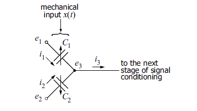
Capacitive half-bridge - currents
Derivation of the formula for the dependence of the output current on the change in capacitance
:
, dq/dt, q=CU, :
, (1.1):
, dq/dt, q=CU, :
, (1.1):
So if you use the same potentials of the input voltages we get the current dependence:
The result is rather strange: the output current does not depend in any way on the change in capacitance. In order to detect a change in capacitance, it is necessary to set voltages of different polarity on the plates, that is: , a ... Then we will redo the equation taking into account this modification.
Dependence of the current on the change in the position of the plate, taking into account the different polarity of the input voltages
1.3:
:
:
1.2 , :
:
:
1.2 , :
From this equation, the following facts are visible:
- if the position of the plates does not change in time, then
- similarly if the signal source constant (DC), then
For the effective operation of the capacitive half-bridge, it is necessary to use variable input signals e1 and e2, the phase displacement between which will be equal to 180 degrees (so that the potentials have different signs). Therefore, we get the following form of signals:
where - the frequency of the alternating signal (determined at the design stage, depending on the system bandwidth and the normal operation of mechanical containers).
So, we got equation (1.4), which shows how a change in capacitor capacitance affects the output of the system. However, such a signal will be quite small in amplitude, besides, if we connect a load to it to communicate with the outside world, the whole system will collapse. An amplifier is needed here ...
Just add an amplifier
Let's add an amplifier to our system (we will assume that the gain is - the principle of the virtual earth works).
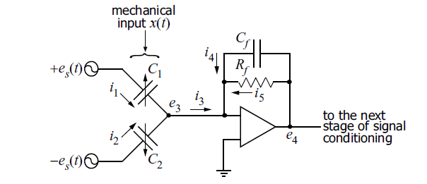
Capacitive half-bridge + integrator
So now we find the dependence of the output voltage of the amplifier on the change in capacitance.
Amplifier output voltage
:
dq/dt, (1.4) :
, x, ( ). , , , ( 1 ). :
, :
, :
dq/dt, (1.4) :
, x, ( ). , , , ( 1 ). :
, :
, :
As a result, we got the dependence of the amplifier output signal on the change in the position of the capacitor plate. The attentive reader should immediately notice that this is amplitude modulation! Indeed, in this system we have a signal x (t), which is multiplied with the signal and amplifies by the amount ... The next step is to remove the carrier frequency , and we get an amplified signal x (t) - which is proportional to the acceleration. A long way of computing has led us to understand the architecture of the MEMS accelerometer.
MEMS accelerometer architecture
Let's first consider the functional diagram of the sensor:
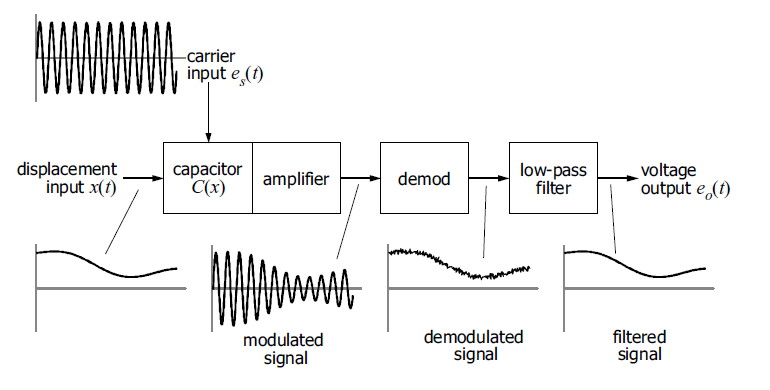
Functional diagram of a MEMS accelerometer.
Initially, we have a signal x (t) - which reflects the change in acceleration. Next, we multiply it with the carrier signal and amplified with an operational amplifier (in integrator mode). Next, demodulation occurs - the simplest circuit - a diode and an RC filter (in reality, a complicated circuit is used, synchronizing the process of modulation and demodulation with one carrier frequency ). Then the residual noise is filtered using a low-pass filter.
As an example, I will cite one of the first MEMS accelerometers from Analog Devices - ADXL50:
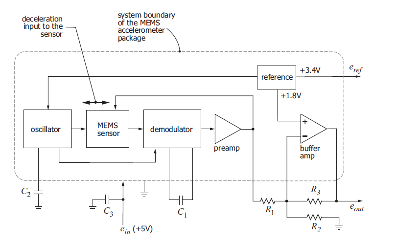
Block diagram of ADXL50
Probably, giving the block diagram of the sensor at the beginning of the article, many readers would not understand the purpose of some blocks. Now the veil is ajar, and we can discuss each of them:
- The block called “MEMS sensor” is a capacitive half-bridge.
- The "oscillator" block generates a signal at a frequency of 1 GHz.
- The oscillator signal is also used for synchronous demodulation.
- , ( VDD/2- , — «»).
- .
- , .
?
The choice of transducer to work with sensors depends on the accuracy you want. To work with sensors, ADCs with SAR or Delta-Sigma architecture with high bit depth are suitable. However, modern sensors have built-in transducers. The leaders in this area are STMicroelectronics, Analog Devices and NXP. As an example, we can give a new microcircuit with a 3-axis accelerometer and built-in ADC - ADXL362.

Block diagram of ADXL362
For working with ADC, anti-aliasing filters have been added to the circuit to exclude additional harmonics from entering the spectrum.
Where can you get such technology?
There are now many factories available for fabless companies that offer MEMS technology. However, to create modern microcircuits, it is necessary to integrate capacities with movable plates into a standard design route, because in addition to such a capacitance, it is necessary to design additional blocks (generator, demodulator, op amp, etc.) on a single chip. As an example, TSMC and XFab factories offer the technology to implement a MEMS sensor along with the entire harness. The picture shows the containers that allow you to create a three-axis accelerometer:
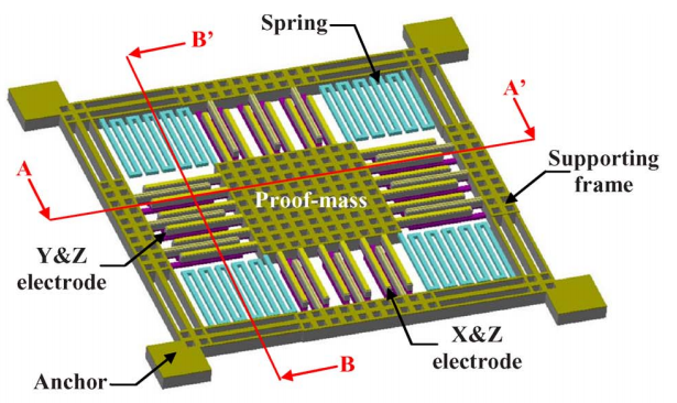
Three-axis capacitive half-bridge from TSMC
There is also a factory for the production of MEMS sensors in Russia - Sovtest , but the enterprise does not have the technology for integrating additional circuitry blocks that are necessary to create the final device and the only way out is to use the microassembly technology.
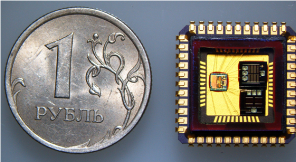
MEMS accelerometer developed by Sovtest
What developments does our company have in this direction?
We have several transducers that are designed to work with sensors. New products include:
- 5101NV035 - 16-channel converter based on 8 Delta-Sigma ADC, designed to work with current sensors
- 1316NX035 - 4-channel integrating voltage-frequency converter (VFC), designed to work with 3-axis accelerometers and gyroscopes.
As I wrote in the previous article , the waiting period for plates from the factory can take quite a long period of time. After the first test run of the 400 MHz ADC, the arrival time of the plates and further measurements took more than half a year. During this time, our team managed to make PNC 1316NX035 (development of the previous circuit 1316PP1U ), which I can tell you a little about.
Voltage-frequency converter
To convert data from the sensor, SAR or delta-sigma ADCs are usually used, however, there is another type of converters - integrating VFCs, which have significant advantages:
- They take up less floor space and have less consumption with the same linearity and noise.
- Simple architecture.
- High immunity to input noise and interference signals.
- Immunity to noise and interference of the output signal.
- The ability to transfer data without processing to a radio frequency communication channel.
The 1316HX035 microcircuit is a four-channel voltage-to-frequency converter and a digital code; the outputs of a three-axis accelerometer are connected to the three main high-precision channels. The 4th channel has an input 4-channel multiplexer, to which additional system sensors can be connected: temperature, humidity, etc. Under a microscope, the circuit looks like this:
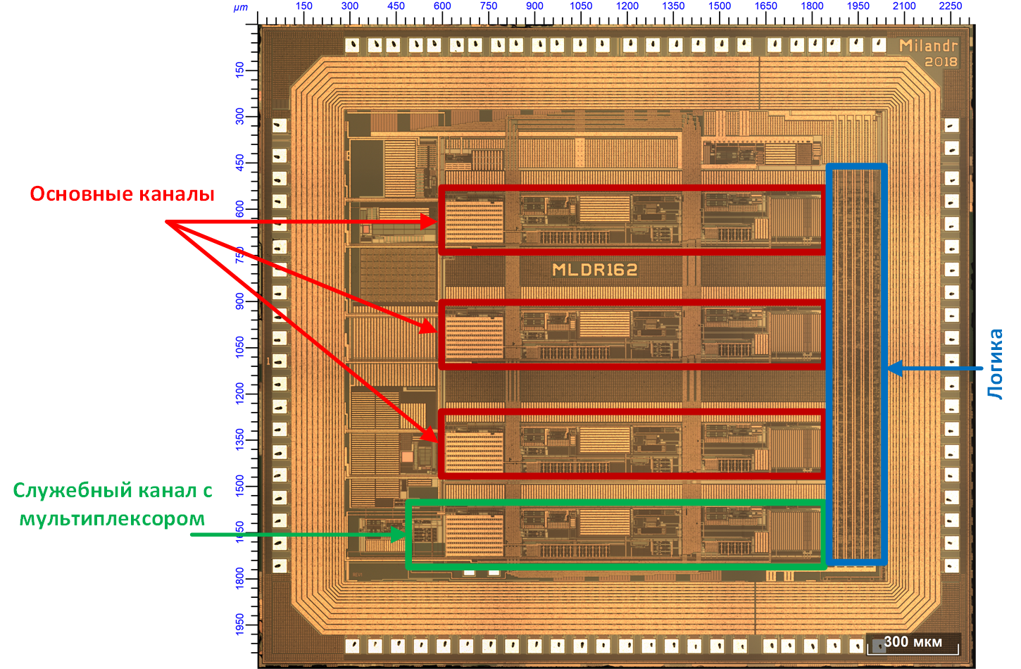
VFC under a microscope
Each of the three main channels converts an input voltage in the range of ± 4V to a frequency of up to 1250 kHz at 3 outputs corresponding to positive and negative input voltages. Also, the microcircuit has a 16-bit reverse counter in each channel for counting frequency pulses. The SPI interface is used to control the conversion modes and sample the contents of the channel pulse counters. The main requirements for the PNC parameters were:
- high thermal and temporal stability of the output frequency at zero input signal (grounded inputs)
- dynamic range of conversion - not less than 22 bits
- continuity of conversion of the input signal and the inadmissibility of the loss of a single frequency pulse.
To meet requirements 1 and 2, analog autocalibration is used , which is performed automatically when the circuit is turned on, and can also be started at any time by command via the SPI interface. Requirement 3 is provided and guaranteed by circuitry solutions. We managed to achieve quite decent accuracy parameters: the typical conversion nonlinearity was 30 ppm, and the zero offset was less than 0.1 Hz with a conversion coefficient of 200 kHz / V. Dynamic conversion range: fmax / fmin = 2 * 1.25MHz / 0.3Hz ∿ 8.33M, which corresponds to more than 23 bits.
There is only one "but" - bipolar nutrition. To ensure good zero stability (voltage that corresponds to 0g acceleration), a bipolar supply must be used. This solution is quite effective - after all, when 0g corresponds to “ground”, the system will be a priori stable. It also improves system design. In modern sensors, half of the Vdd / 2 supply is used as zero, however, if the voltage at the converter differs from the voltage at the sensor, we automatically get an offset that needs to be additionally calibrated.
Probably, for many consumers, bipolar voltage scares a little, and we, as developers, understand this. Perhaps in the future we will make a commercial version for MEMS (or integrate the sensor into the PNC). So far, of course, these are just plans, but I'm sure they will see the light of day.
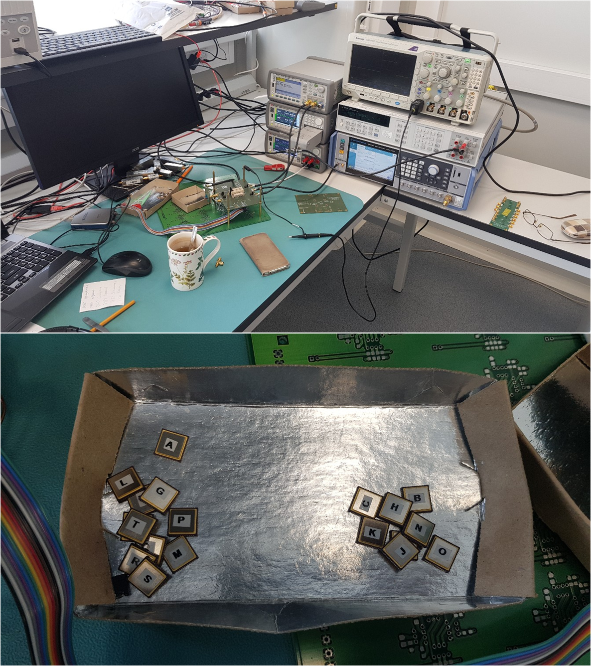
PS Found bonus photos from the sample research process. In general, this, as for me, is the most interesting part of the development process. They give you in your hands your brainchild in the heat of the factory, you supply it with power and cross your fingers you wait - "does it work or not?"
PPS Whoever liked the topic of sensors, in the future a colleague from the hardware design center would like to talk about the inertial system being created based on MEMS sensors - SINS .