Let him say to me:
"You are an old donkey, you did not live like this, I will live differently."
I understand, but let him say! But he is silent.
Recently, one of my young colleagues (MMK) asked me to see the misunderstandings going on in its development. The product was a 5V to 5V step-up converter, the main purpose of which was to compensate for the voltage drop on the cable for connecting an external DVD drive to the USB interface. The converter was built on the basis of the MAX669 microcircuit in the "self-support" mode, the circuit corresponds to the recommended one and, nevertheless, the device did not work - the output voltage was 4 V, that is, the power supply was 5V minus the drop on the wires, minus the forward drop on the diode.
We look at the oscillogram at the gate of the transistor, we see 90% filling there with a signal amplitude of 4V, but the transistor does not open. It should be clarified here that MMK used domestic transistors of the 2PE208A type. The transistors themselves are not bad, the parameters are quite decent, but the opening voltage is, according to the specifications, from 2.5V to 4V, so the transistor has the right not to open at 4V on the gate - mea maxima culpa.
Yaroslavna's first cry (nYa): as I said above, the transistor parameters are quite decent, but (of course) there is one small drawback (at least in the documentation) - if the static parameters are specified in the required volume, then the dynamic parameters (with the exception of the generalized capacity shutter) are indicated a little more than nothing. Moreover, the on and off delay time itself is in the documentation and the specific transistor behaved quite well in terms of speed (when we increased the input voltage so that it began to open and the circuit began to work), but these parameters are given in the technical specifications in the section “reference data ", Moreover, they are referred to as" typical values ", that is, it is impossible to rely on them when designing a device," from a word at all ", which sharply limits the possible scope of the above components.The reason for such a decision by the developers of transistors remained a mystery to me, if any of them read this post, explain in the comments.
Okay, we change the transistors to imported (import substitution failed) of the IRF7103 type (they were just at hand) with an opening voltage of 1.0V to 3.0V, the circuit starts working, but somewhat strange - the gate is still 90% filled, the transistor works, but the output voltage is 3.5V, while almost 2A is consumed from 5V. We turn off the drive, the picture does not change, consumption is concentrated in our product. We see that the TUSB9261 microcircuit, which is responsible for converting the USB interface to IDE, heats up, we start looking at the oscillograms on its legs, starting (of course) from the clock generator and ... the external consumption miraculously decreases to 0.2A. We repeat the switch on, again we see a defect, we solder the capacitors at both ends of the quartz resonator and the board starts to turn on normally - mea culpa.
: , , , (RC ) , — Texas Instruments. , , , .
We turn on the board again - the output voltage is stabilized at 5V, connect the drive and turn on again - the output voltage becomes equal to the required 5V, but after a while it drops to 3.5V, then it is restored and the cycle repeats. Instead of USB power, we connect the output of a stabilized laboratory power supply (LIPS) and observe a sharp jump in the current consumption at the time of starting the drive motor from 0.3A to 1.2A. Yeah, of course, the guaranteed supply current of the interface cannot be higher than 0.5A, you need a second cord to double the current, well, this is a common practice, mea maxima culpa. It seems that everything is clear and working, we decide to conduct a series of experiments to determine the dynamic parameters of the source of the device under development using LIPS and a guaranteed load in the form of a 4 Ohm resistor.
We supply voltage from the LIPS to the device input not by sticking bananas, but by turning on the output voltage of the source with the connected device. Generally speaking, this method of verification cannot be recommended for arbitrary LIPS, some of them, for example, Yerevan ones (I don’t remember the brand, now, of course, they can no longer be found) at the moment of switching on gave an overshoot with a surge of up to 40V, but in this LIPS we are confident so we can afford it.
: , . — , ( , ). , , .
And, quite unexpectedly, we find that the device does not go into operating mode, but everything turns out to be in the same incomprehensible state, and the LIPS stabilizes the supplied current at 2.2A, dropping the voltage to 3.2V. In this case, we observe 3.5V at the output, despite the fact that the duty cycle is still the same 90% and the transistor switches stably. It turns out that the voltage rise factor is 3.5 / 3.2 = 1.1, which is clearly less than the expected 1 / (1-0.9) = 10 and the efficiency of the source is (3.5 * 3.5 / 4) / (3.2 * 2.2) = 43% and this is frankly a little ... There is a clear manifestation of black magic (energy goes nowhere) and violation of the laws of electronics. Since at first glance, there is no reason to say mea culpa, and even more so mea maxima culpa, let us investigate the problem in detail and start with theory.
The diagram of the power stage of the boost converter is shown in the following figure, the
theory of its operation has been discussed in numerous materials (I personally really like the course of Robert Erickson, where the picture is taken from), we use the results without output (everyone can find it in the mentioned source or get it on their own - strongly I recommend the second method). And the main result is that the converter is capable of increasing the voltage to infinity (according to the formula 1 / (1-d)) only “in a spherical vacuum” and only if its work is not interfered with by “vacuum clots”, but in real a circuit with real components has a limiting voltage rise factor
Kmax ~ 1/2 * sqrt (R / (Rl + Rds)) and it is achieved at a duty
cycle d = 1-sgrt ((Rl + Rds) / R).

: , «» , d, , , , … ( , ) , .
( ) , « ».
For the case under consideration, Rl = 0.17 Ohm and R = 4 Ohm, we have Km = 2.4 and the corresponding d = 0.8. It seems that this is enough to increase the voltage to 5V with an input voltage starting from 4, but from 1.8V, when the regulator in the MAX669 controller microcircuit starts working, not everything is so good, but we do not need such low input voltages. But we did not take into account another source of losses (or rather, two, the second is the resistance of the diode, but it is of little significance in this case) of the transmission coefficient, namely the drop across the open transistor.
What nonsense, you say after the MMK, the selected transistor has Rds of the order of tenths of an ohm (specifically 18mOhm) and cannot significantly affect the operation of the circuit, but you will be wrong. Unfortunately, many manufacturers of transistors give this figure when the voltage at the gate relative to the source (control voltage) is significantly higher than the opening voltage. In specific technical documentation (TD), we see the maximum gate / source voltage (opening voltage) 2.5V (in my other post I showed why we should take the maximum value of this parameter, and not the minimum and, moreover, not the typical ... Satan), and a resistance of 18 mOhm is given at a control voltage of 10V.
Meanwhile, it is widely known (although, unfortunately, not as widely as we would like) that the resistance of an open field-effect transistor (as far as it is appropriate to talk about it, since this indicator of a real transistor is clearly nonlinear) is inversely proportional to the difference between the control voltage and voltage opening. That is, with a control voltage of 3.5V, we will have a switch resistance of (10-2.5) / (3.5-2.5) = 7.5 times more than indicated in the TD, 18 * 7.5 ~ 140 mΩ, which is quite comparable to the resistance of an inductor.
But at 2.5V control voltage, and even more so at 2.5-0.4 = 2.1V (we have a "self-support" circuit), the transistor generally has every right not to turn on, let's remember this for the future.
Now we can refine the maximum parameters attainable and get
Kmax = 1/2 * sqrt (4 / (0.17 + 0.14) = 1/2 * sqrt (12.9) = 1.8 (achieved at d = 0.72) and two terrible facts become obvious:
1 - about the voltage increase to the required rating at the input 2.5V you can not even dream of;
2 - the fill factor is more than 0.72 is unacceptable.
If the problem associated with the first fact is obvious, then the influence of the second should be discussed in more detail and we will do this a little later. But first, we will correct the mistakes made - replace the inductance with more suitable with a resistance of 60 mOhm and a transistor on CSD16342Q5A, in which the public key resistance is 12 mOhm at a control voltage of 2.5 V (maximum opening voltage of 1.1 V). Then the expected
Kmax = 1/2 * sqrt (4 / 0.06 + 0.012) = 3.7 and it is achieved at d = 0.94, so we can count on a completely stable operation of the converter, starting from the input voltage (5 + 0.6) /3.7=1.5V.
Not quite pY, so no number: finding a transistor on the TI website with the required guaranteed resistance at a low control is not as easy as it could be in an ideal world with ideal sites. You can sort the required transistors by the average opening one, and then you will have to open the transistor one by one and look at the corresponding technical documentation. And on an ideal site, I could ask for an additional parameter "Minimum Rds at Ugs = 2.5V" and get an answer right away.
Indeed, after replacing these elements, the step-up source begins to work normally and provides 5V / 1.2A at an input voltage of 2.5V to 5V. Note that the operating input voltage actually turned out to be higher than the calculated one due to the peculiarities of the control microcircuit, which, in the range from 1.8 to 2.5V, operates with a fixed duty cycle of 0.5 and only then begins to regulate the output voltage. Note also that we cannot guarantee that the converter will work below the calculated values, regardless of the behavior of a particular instance (s).
You ask, how do we manage to get 5 out of 5, because we have a step-up converter - in fact, we get 5.4-5.8 (depending on the load current) and after the diode the voltage drops to the required 5V.
Now everything is fine and the problems have been solved - unfortunately, not completely. If everything were exactly like this, I would not write a post with a story only about my mistakes (so far, apart from them, we have not fixed anything). We return to the original components of the circuit, because they guaranteed us to work with an input voltage of 3V, and with an input voltage of 3.2V we find ourselves in our "favorite" mode - a duty cycle of 90%, an output voltage of 3.5V, an input current of 2.2A. Yes, with "more correct" components, this phenomenon was not observed, but then what are the boundaries of the "correctness" of the components. We will consistently answer the main questions.
"Who is guilty".
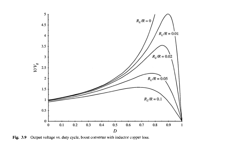
Once again, let's take a close look at the graph of the change in the output voltage depending on the duty cycle (duty cycle) and find two sections on it - an upward and a downward one (our case is 0.05). If we draw a straight line corresponding to the required output voltage at a fixed input voltage, then we will see two points of intersection with this graph (perhaps one or none at all, but these are frankly not operating modes) at which the required conversion factor is achievable. Nevertheless, only the point located to the left of the maximum (with a lower duty cycle) is working on the following bases:
1) the regulation law embedded in the microcircuit implies a direct dependence (the more, the more) the regulated parameter (output voltage) on the regulating parameter (duty cycle), and in the descending part of the curve the dependence is inverse, which would be half the trouble if it were not for the following circumstance ;
2) if we plot the efficiency of the boosting source depending on the duty cycle, we will see that its value decreases as the duty cycle increases over the entire range of determination, at first smoothly, so that at the maximum conversion point, the efficiency is 50%, and then it is simply catastrophic up to to zero. It is quite obvious that if it is possible to obtain the same output voltage with an efficiency of 80% or 20%, then the second option should not have prospects for practical implementation.
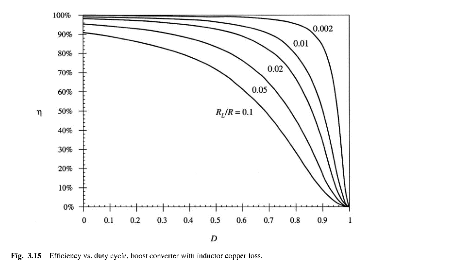
This effect is explained by an increase in the drop on the parasitic resistances of the choke and transistor, and the drop grows clearly nonlinearly, because the current through these components is associated with the output current, which increases with increasing output voltage through the conversion factor - duty cycle. I have already indicated the methods of struggle above - reducing parasitic resistances, but now we are not talking about that.
So, we made sure that you should not increase the fill factor above a specific value determined by the load parameters and the real parameters of the circuit components. However, the IC can provide a control signal with a duty cycle of up to 90% if deemed necessary. And precisely in connection with this feature, given the ability of the microcircuit to work, starting from a voltage of 2.5V, we are faced with a very unpleasant process called "snapping".
"How does this happen".
Failure scenario:
1. Turn on the LIPS when the converter is connected with a load, the voltage at its output starts to slowly rise, up to voltage 1.8 nothing happens.
2. With an input voltage of 1.8 to 2.5, the microcircuit generates a control signal with a duty cycle of 50%, the transistor may start to operate (or may not start, as luck would have it), the output voltage rises, although its value is not known.
3. After reaching the voltage of 2.5, the microcircuit begins to control the converter, trying to reach the output voltage of 5 + 0.6V, for which it is required to have an increase in voltage of 5.6 / 2.5 = 2.24 times, which obviously exceeds the limit set by us. Therefore, the duty cycle reaches a maximum value of 0.9, the output voltage becomes 2.5 * 4 * 0.1 / (4 * 0.1 * 0.1 + 0.17 + 0.14) = 2.8V, while the efficiency is less than 20%.
4. The input voltage rises further, along with it the output voltage and output current (and with it the input current), at some point the input current (nine times the output, by the way) exceeds the protection limit and the LIPS goes into current stabilization mode. So we have come to our "working point", in which we will be for an infinitely long time.
PNP: And this is the best scenario, because if we do not have current protection on the LIPS, then after the input voltage reaches 5.6 / 1.12 = 5V, the microcircuit will see that the voltage has become more than the required one, will begin to decrease the duty cycle and return to the left side of the adjustment curve, having previously passed through the peak 5 * 1.8 = 9V with unpredictable consequences for the supplied components.
"What to do".
Since we are not sure of the correct (more precisely, we are sure of the incorrect) operation of our circuit at low (less than 3V) supply voltages, we should take measures not to let the circuit at low input voltages into the right side of the curve, we will indicate possible ways to do this:
0) “We smile and wave” - we pretend that nothing terrible is happening and that food will always be supplied in a “jump” and there will be no failures - well, in general, you understand why water parks collapse, rockets explode, planes uncontrollably go to dive, and cars accelerate uncontrollably.
0 *) "The problem is not at our end" - we explicitly require in the technical documentation a "jumpy" power supply and the absence of voltage drops below the operating voltage. The method is clearly better than the previous one, we did not hide the problem under the carpet, but clearly indicated it. Another thing is that no one will put a power “purifier” specially for us (I'm not sure that this requirement will be paid attention at all) and it will not be easy for us to prove that the requirements for connecting our product have not been met. Nevertheless, there is a fundamental opportunity to relieve oneself of responsibility for the incidents that have occurred, although this will not make it easier for the victims.
1) “If you have to pay, a gentleman always pays with a smile” - we select circuit components with a large margin, ensuring operation at low voltages. The method is understandable and we went with it, at the same time we raised the efficiency in the operating mode a little, but "you have to pay for everything in this world" and we will have to increase the weight and dimensions and / or the cost of our product.
PNP: In this case, it is imperative to take into account that the restrictions still remain, just their boundaries have shifted. For the considered replacement with an inductance resistance of 60 mΩ, a transistor of 12 mΩ and the need for normal operation at an input voltage of 2.5, we obtain Kmax> = 5.2 / 2.5 = 2.24, then the limiting load resistance R> = 4 * Kmax * Kmax * (Rl + Rds) = 1.44 Ohm, or, in other words, the current consumed from the converter must not exceed 3.5A in all modes, including at the moment of switching on. It is clear that it is better not to approach the dangerous limit and make one and a half or even two-fold protection for critical parameters, but this is to your taste.
2) “You cannot control the wind, but you can quite control the sail” - block the error, that is, exclude the possibility of supplying low input voltages to the input of the converter. We cannot guarantee the behavior of an external source, but we can control our input circuits. The method is good, but it requires circuit correction, so not now.
2 *) prohibit the operation of the circuit at low input voltages - the direction looks more promising than the previous one, since no power elements are required and especially given the presence of a permission input in the microcircuit. But not now, like the previous method.
PNP: you can implement blocking of work in different ways: here is a resistive divider and the use of a zener / three-lead zener diode and a bipolar transistor with the formation of an opening voltage in the above ways and a real comparator and so on ... thousands of them.
The only thing that is unacceptable is the RC circuit, since this circuit does not solve our main problem (I remind you that this is the prohibition of the circuit operation until a certain value of the input voltage is reached), but some other (the formation of a given time interval after reaching a certain voltage that does not coincide with the controlled one) and refers us to option 0 *. At the same time, such a chain can be useful after the comparison circuit of the above type to eliminate bounce near the switching point.
PNP: If you decide to use an RC circuit, do not forget to provide a capacitor discharge circuit by shunting either a resistor or a capacitor with a diode, otherwise power failures will prepare us a lot of "wonderful discoveries" with a negative emotional background.
Well, here comes (my regular readers were already nervous, completely in vain, it happened) the lengthy fifth point: it cannot be said that the developers of the microcircuit did not know about the possibility of such behavior of sources based on it, as evidenced by the following sentence from the technical documentation
“Other (undesirable ) characteristics of bootstrapped operation are… reduced ability to start up with high load current at low input voltages ", which I tend to translate as
"An undesirable aspect of self-sustaining operation ... is the reduced ability to start with high load currents at low input voltages."
In my opinion, such a warning is completely insufficient and a link to the application note is required, in which the content of this post should be a small part.
For example, in the section "Selecting inductance", the resistance requirements are not mentioned at all. It is clear that these requirements must be known to the engineer, but then the requirements for the minimum inductance must not be less known to him, and the latter are accurately presented in this document.
Well, and like a cherry on top - the documentation has a section "choosing a transistor", which says about the need to take into account the need to work at low voltages, while in the same document they give a typical boost converter circuit for an output 12V / 0.5A (or 5V / 1A, just our case), indicate the input voltage range of 1.8-5V on the diagram and completely forget that:
1) up to 2.5V, the microcircuit operates with an unregulated duty cycle of 0.5, so the output voltage will be no more than 5V, which is somewhat different from 12V (and not even equal to 5V);
PNP: I am generally somewhat surprised by the positioning of the microcircuit (throughout the text of the document, starting from the title), as ready for work, starting at 1.8V, which is completely untrue, the minimum operating voltage of 2.5V would be more correct.
2) the used transistor of the FDS6680 type has every right not to open until a control voltage of 3V is received, and given the presence of a diode in the "self-supported" circuit, this is a minimum 3.5V input voltage, which is clearly more than the specified minimum input 1.8V.
Pnp and at the same time the sixth pYa: at first I thought it was just a mistake (yes, this happens to everyone, not only me and MMK), but one small circumstance made me change my mind. This circumstance lies in paragraph 5 of the section "choice of transistor", namely:
«5) Minimum threshold voltage (VTH(MIN))». , , , . , . , , .
By the way, the second IRF7401 transistor recommended for use in its technical documentation gives exactly the minimum threshold voltage (0.7V) and no more, which is somewhat alarming. I cannot exclude the option when the maximum threshold (well, typical, I do not mind to be indicated in the documentation, I only mind to be used in the calculation of the circuit) coincides with the minimum, but I would like to see this information specified in the documentation explicit in a way, since a different approach drives us to the "shaky ground of guesses and assumptions", and it can in no way be a reliable foundation for honest engineering work.
If the authors of the documentation criticized in the post (or their sympathizers) have something to say
Well, the exposure of black magic took place, as always, we found a natural-scientific explanation for the observed behavior of the scheme (as one remarkable character said: “I am a materialist”) and we did not have to go over to the dark side. I hope that my notes turned out to be useful to someone in practice, or, at least, entertained in the process of reading.