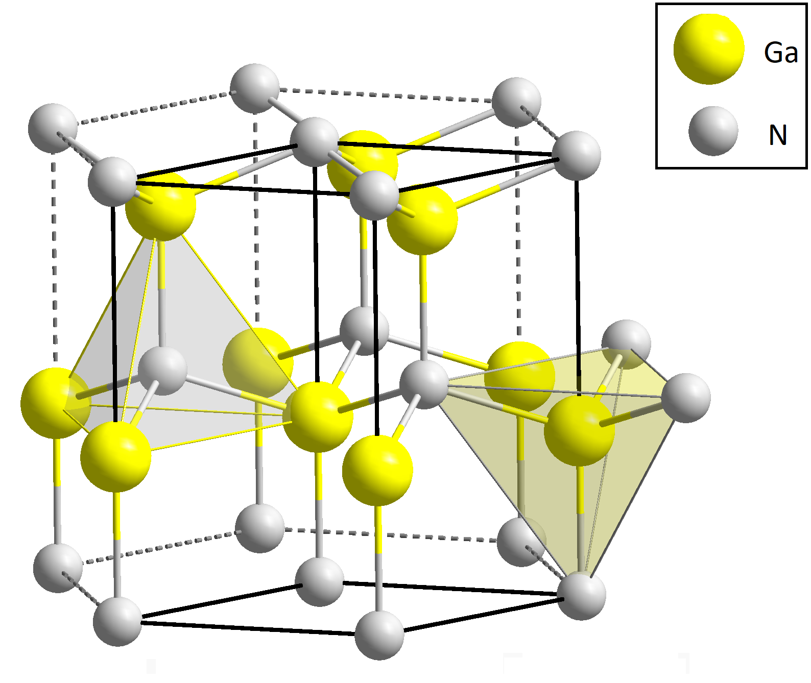
Meet gallium nitride. Isn't he handsome? Image: Solid_State / Wikimedia Commons
At the dawn of the formation of Habr, we admired the HTC HD2 smartphone: its 4.3-inch diagonal seemed to be something incredible, and its 1200 mAh battery aroused sincere respect. Today, of course, these numbers cause only a smile: flagship screens have doubled, and batteries have tripled. Along with the growth in performance, the number of cameras and battery sizes, the popularity of fast charging technology is also growing, which is not surprising - if a 5 W adapter was enough for a 1500-1700 mAh battery, then by now the market is full of smartphones with batteries of more than 4500 mAh.
The Quick Charge and Power Delivery standards have partially solved the problem, as well as a large number of proprietary variations on the topic of accelerated charging from smartphone manufacturers. Of course, this required special charging controllers and complex algorithms (no one wants to short circuit a lithium battery, as was the case with the Galaxy Note 7). All methods of accelerated charge replenishment in one form or another relied on increasing the power of the charger: by increasing the voltage or operating current. A side effect of such innovations was an increase in the operating temperatures of circuit elements and the size of the power supply. And then a new material came to the rescue - gallium nitride (GaN), which has already been used in semiconductors and microelectronics.
What is gallium nitride and why is it needed?
Most current semiconductor elements have used silicon for decades, one of the most common elements in the periodic table. It is relatively easy to work with and in most cases its characteristics are sufficient to ensure the working properties of the products. Unfortunately, there are also areas of application where the capabilities of this material have become a "bottleneck".
In a nutshell, the usefulness of gallium nitride can be described by the following example: in a switching power supply, the target voltage is obtained by repeatedly turning on and off transistors (passing or turning off current in the circuit) with a given timing. So, when a classic silicon transistor is switched from a conducting state to an insulating state, a large amount of heat is released, which reduces the efficiency of operation and limits the use of such elements in powerful power supplies.
 A blue semiconductor laser typically uses gallium nitride or an indium alloy to produce the desired wavelength. Photo: Pang Kakit / Wikimedia Commons
The main advantage of gallium nitride lies in a key characteristic of a semiconductor: the band gap. In a broad sense, the "forbidden band" indicates the difference in the energies of an electron, which distinguishes a current-conducting state from a valence (ie, non-conducting) state. With increasing temperatures, the characteristics of the semiconductor change, because thermal vibrations of the atoms of the material increase the energy of the electrons and "knock" them into a conducting state.
A feature of GaN transistors is an extremely wide band gap - 3.40 eV versus 1.12 eV for silicon analogs. In power circuits (which are especially susceptible to heating during operation), this advantage allows you to maintain constant performance characteristics and not reduce efficiency at higher temperatures. In addition, due to the high charge carrier density, GaN transistors can withstand much higher currents. And in general, gallium nitride crystals themselves are more resistant to high temperatures.
Everything new is well forgotten old
The first studies of its properties began in the 40s of the XX century, and already in the mid 90s of the last century it began to be considered as one of the most promising optoelectronic materials. It should be noted that it was in optoelectronics that he found wide application in the first place: gallium nitride is one of the few substances capable of generating radiation in the blue spectrum. Therefore, it is used, for example, in those very lasers for Bluray drives. They also want to use it in UV-resistant solar cells, but this can be a separate story.
GaN-based structures have proved to be suitable not only for optical devices. The characteristics described above turned out to be useful for the development of the component base of power and microwave electronics, including transistors. Another important nuance that allowed gallium nitride to seriously claim universal recognition was the price and safety: the previously occupied gallium arsenide (a compound of gallium and arsenic) is extremely difficult to produce; in addition, GaAs can form toxic and carcinogenic compounds.
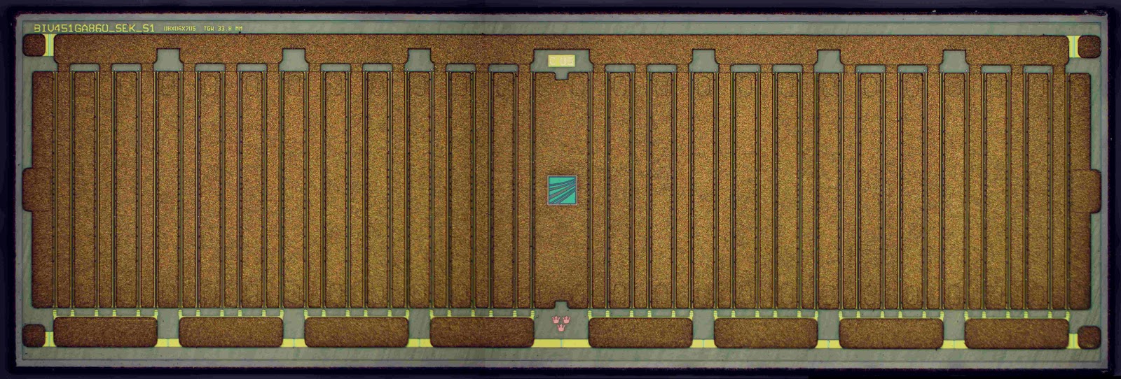
 A micrograph of a high-speed GaN transistor operating at 100 volts. Photo: Fraunhofer IAF
Yes, today silicon semiconductors are cheaper due to the fact that the process itself has been thoroughly studied, production is fine-tuned, and raw materials are much more affordable. However, even with such reservations, the difference in cost does not reach significant values and has little effect on the price of the final product. If we talk about the future, then a large-scale transition to GaN promises to save money at all by reducing power consumption by 10-20% in comparison with electronics with silicon transistors.
Practical use
Since the only way to reduce the heating of transistors is to make them work not at full strength (i.e. take the element base with a large margin), powerful silicon-based switching power supplies are of impressive size. The ability of GaN transistors to operate at high temperatures and the compactness of such models can significantly reduce the required volume of the case for placing and cooling the filling. For example, the size of a power adapter for a laptop or smartphone can be reduced by about half while maintaining performance. The opposite is also true: you can keep the overall size of the memory and improve its performance.
 And really more compact - with the same power. Photo: Anker
The reasons why this becomes possible lie on the surface. The high density and wide band gap of gallium nitride can significantly increase the efficiency of final devices. While for silicon transistors even 95% is considered very decent, for solutions based on GaN it reaches 98–99%. Taking into account the power of modern power adapters, this significantly reduces the amount of heat generated, which acts as a limiter for the operating modes of silicon semiconductors. And the aforementioned ability of GaN components to operate at higher temperatures allows you to squeeze out a little more power, all other things being equal.
Of course, the transition to gallium nitride does not mean some kind of revolution, especially if we consider it in the context of chargers for gadgets. By and large, such an "upgrade" only brings them closer to the capabilities and needs of modern smartphones, which are in dire need of high-power adapters. Therefore, there is nothing surprising in the fact that manufacturers of mobile equipment could not pass by promising material.
 Image: Anker
Almost all major vendors are currently engaged in their own research on the use of GaN in chargers for their devices, and its upcoming mass use is beyond doubt. However, in order to personally appreciate the delights of gallium nitride power adapters, you don't have to wait several years. There are already Anker chargers on the market that have been taking advantage of GaN for several years.
Anker and GaN
Anker has been specializing in the development and production of chargers for a long time, and it was simply impossible for us to pass by such a promising material. Assessment of the prospects for gallium nitride made it possible not only to use it in creating powerful chargers, but also to create a truly universal power supply suitable for smartphones and laptops with Type-C power supply. Add to this support for several fast charging protocols at once - and with such a power supply, the user will be able to charge almost any gadget quickly and efficiently, regardless of the brand.
The result of the work of our engineers was the emergence of a whole line of Anker Atom adapters using GaN transistors in the power section. It all started with a single charger in 2017 - and now the family has expanded to include several solutions at once. For example, the Anker Atom PD1, with dimensions comparable to standard 10W chargers, delivers up to 30W of power output and is Power Delivery compatible. It is optimized to work with the latest iPhone and Samsung models, allowing you to charge these gadgets at an increased speed. Compared to the stock charger of the same iPhone XS, it provides more than double the charging speed. It can also be used to charge MacBook Pro and Air laptops.
 PowerPort Atom III 60W Dual Socket Charger Image: anker.com
For users of more power hungry laptops, there is an advanced model - Anker Atom PD2. It is slightly larger than the miniature Atom PD1, but is capable of delivering up to 60 watts of power when charging a single device. Or provide a couple of gadgets at once with power up to 30 W - thanks to two connectors on the case and a parallel power supply circuit.
Also worth noting is the Atom III 60W charger. It is also available in two versions - with one and two connectors and support for fast charging technologies in three popular formats: Apple Fast Charging, Samsung Fast Charging and USB-C Power Delivery.