The importance of the thermal problem can be seen in a simplified rule of thumb that says that every temperature increase of 10 on the C shortens time to failure by 2 times. That is, if at 55 on a chip will last 10 years, at 65 about With only 5 enough arguments to somewhat improve the heat dissipation from the chip, if not to play in planned obsolescence. This rule is far from being the ultimate truth, but it is qualitatively correct (you can read more, for example, here ).
The organization of the heat sink is almost always an overhead process that complicates the routing, so it must be planned in advance. To do this, you need to understand whether the printed circuit board itself can handle the heat sink. Chip manufacturers indicate in the documentation the parameter "crystal-medium" thermal resistance R θJA . It would seem:

and the estimate is ready. But this is rude, very rude. Thermal resistance is highly dependent on the PCB. And what is indicated was obtained in an experiment on a standardized printed circuit board (for example, as in Figure 1), which, most likely, will be very different from what you get. Let's just say you can get a much better heat sink in a smaller footprint.

What is worth paying attention to is the die-to-board thermal resistance R θJB or R θJC (bottom) . This is something that no longer depends on the developer and is determined by the body and its internal design. But here, most often, the choice of a case is determined by the heat loss power, and the main temperature difference will be on the board. So, we rewrite the above formula for the case of heat dissipation through a board as follows:

where R θBA is the thermal resistance of the printed circuit board with the given parameters. You can calculate this resistance based on a beautiful model,


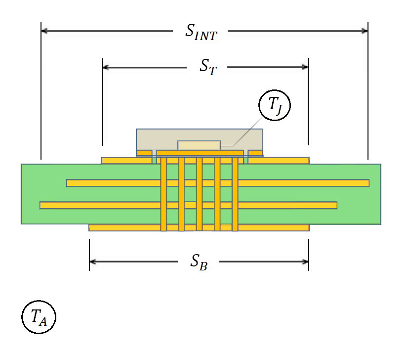
Everything with this equation is fine (except for the modified Bessel functions), and it can be solved for one surface with convection (removing the "2" at the root), but only the boards are most often without radial symmetry and not homogeneous, but also heat is supplied unevenly along the internal radius. So you need to adapt. The first two questions are solved by dividing into annular zones with homogeneous properties with the same area. To solve the latter, you need to build an approximate model of the thermal resistance circuit. Figure 3 shows what was suggested in the original article. It is proposed to beat the board into three zones: the zone under the microcircuit, the zone with polygons on the outer layer, and the zone with only polygons on the inner layers. Only conductors that are directly connected to the microcircuit are taken into account (conditionally, "ringing").

It is proposed to average the upper and lower polygons and take the average metallization area. I do not really agree with this, since the effect on heat dissipation of these layers is obviously different, plus they can differ greatly in area (the lower one will often be larger in area). Therefore, I split the board into upper and lower halves and did the calculation for each part separately.
The article contains many graphs with the influence of various parameters, it is useful to look at them. I calibrated my approach to splitting the board on these graphs (Figure 4) - they are for the QFN5X5, QFN6X6 and QFN3X3 packages, respectively. When the board is very large, the graph "falls" on the limit associated with the thermal resistance of vias, but their parameters are not specified. I took a diameter of 450 microns, a wall thickness of 20 microns, without filling.


It can be seen that the models are correlated, but I did not try to achieve 100% coincidence, since all the input data is still missing. In addition, there is a strange moment with vias (Figure 5), their absence practically does not affect the thermal resistance, which is not very intuitive.
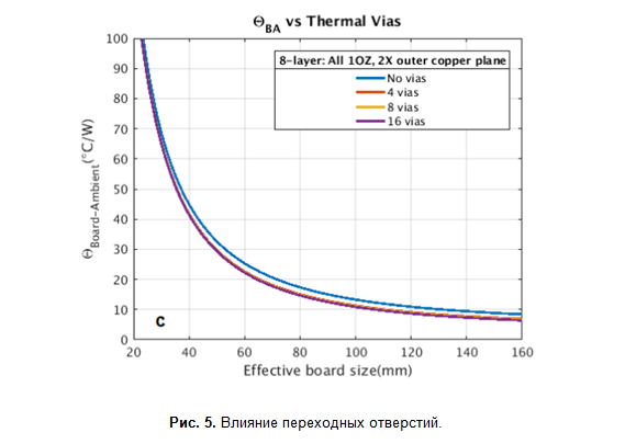
Even in the lower graph in Figure 4, you can see two rows of data, where I counted the two-zone model by two methods: using matrix multiplication, as described in article AND8222 / D, and using a model, as in Figure 3, only the zone under the microcircuit is thrown out (it does not contribute to resistance). It can be seen that the graph from the article goes to approximately the same asymptote, as if the influence of vias is absent. This for me became another factor that something is wrong in their model, taking into account the influence of vias (or I don't understand something).
The calculator turned out to be useful at least in the sense that it made it possible to move from qualitative ideas about the influence of various parameters to quantitative estimates. It can be concluded that the thermal resistance of the board can be driven into the region of 10 oC / W even with natural convection. For dissipation, 2-3 W will be sufficient. Another useful note is that only the metal directly connected to the microcircuit plays a significant role in the heat sink. Although, of course, the larger the volume fraction of copper in the board, the higher the effective thermal conductivity will be. Based on this calculator, you can increase the presence of a heatsink on a microcircuit and a heat sink to the case, I will also do this. If there is something interesting, I will share it in the next publications.