One In 1974, Hewlett-Packard developed a microprocessor to control various functions in its products, from floppy disk drives to voltmeters. This simple processor was not up to standard microprocessors - it didn’t even support addition or subtraction - so it was called a "nanoprocessor." The key features of Nanoprocessor were low cost and high speed of work: compared to the modern Motorola 6800 costing $ 360, Nanoprocessor cost $ 15, and the control operations were much faster.
Although it did not have an addition operation, Nanoprocessor could (slowly) add numbers by repeatedly incrementing or decrementing (the operations it supported). In other cases, for example, with a voltmeter from Hewlett-Packard, ALU chips (74LS181) were added to the product, which were engaged in quick addition - they were accessed as I / O devices. Naturally, being Turing complete, Nanoprocessor could theoretically do everything from computing floating point functions to launching a Crysis game; it just would be very slow.
The processor photo template can be downloaded from the link (122 MB PSD).

HP Nanoprocessor, 1820-1691. , -2,5 , – . , .
In the following decades, the processor remained unknown until recently its developer, Larry Bauer, shared the photomasks and documentation for the chip with The CPU Shack project. There they scanned the photomasks and wrote an article about Nanoprocessor. After Antoine Berkovichi stitched the images into one, I wrote a review of Nanoprocessor based on it . This is the second part of the article, where I discuss some of the details of the Nanoprocessor circuit, doing reverse engineering based on photomasks. The functional blocks of Nanoprocessor are interesting to study because it bypasses the minimal implementation of the necessary functions, while remaining a useful microprocessor.
Inside Nanoprocessor
Like most processors from that era, the Nanoprocessor is 8-bit. However, it does not support random access memory, and the code is executed from an external 2KB ROM. It has 16 8-bit registers - more than most processors and enough to make up for the lack of memory for many applications. The Nanoprocessor had 48 instructions - significantly fewer than the 72 instructions for the Motorola 6800. However, the Nanoprocessor had a handy set of bit set, clear, and check operations that other processors of the time lacked. It also had several I / O commands that supported both I / O ports and general purpose I / O pins, making it easy to control other devices with it.
Nanoprocessor did not have instructions to support memory handling, as it was designed for operations that did not require data storage. However, in some applications, the Nanoprocessor used RAM as an I / O device. An address was sent to one of the I / O ports, and a byte of data was read from the other. Nanoprocessor combined photomasks (clickable) From the above photomask image, we can conclude that Nanoprocessor is simple. Blue lines are metal conductors on top of the chip, green ones are silicon with impurities. Black squares around the perimeter - 40 sites for communication with external contacts of the IC. The small black areas inside are transistors. If you look closely, you can count 4,639 of them.
If we take into account that the instruction decoder consists of pairs of small transistors, which is done for the convenience of the arrangement of components, and count these pairs as one, then we get 3829 transistors. Of these, 1061 are pull-ups, and 2668 are active. By comparison, the 6502 had 4,237 transistors, 3,218 of which were active. The 8008 had 3500 transistors, while the Motorola 6800 had 4100.
The block diagram below shows the internal structure of the Nanoprocessor. In the middle there are 16 holding registers. The comparator allows you to compare two values to provide conditional branching. The control logic unit deals with the increment, decrement, shift, and bit operations of the accumulator. It does not have the arithmetic and logical operations of the standard ALU. The program counter (right) retrieves an instruction from the instruction register (left); interrupts and subroutine calls have their own one-item stacks to store return addresses.

Flowchart of work from the instructions for Nanoprocessor
Let me emphasize that, despite its simplicity and lack of arithmetic operations, Nanoprocessor is not some kind of "toy" processor that switches control lines. It is a fast and powerful processor used to perform complex operations. For example, the HP 98035 real-time clock module used Nanoprocessor to process two dozen different ASCII control strings, as well as to count the number of days in a month.
An interesting project for fun can be the creation of an FPGA version of Nanoprocessor - since Nanoprocessor is perhaps the simplest version of a real commercial processor. The instructions for it describe all the commands and give examples of code that you can run.
Registers
The photo of the crystal below shows that a significant part of the Nanoprocessor is occupied by its 16 registers. They communicate with the rest of the components via the data bus. The chains at the top pick a particular register. Register R0, on the right, next to the comparator.

A significant part of the Nanoprocessor is taken up by its 16 registers.
The building block of a register is two inverters in the feedback loop, storing one bit as shown below. If the top conductor is 0, the right inverter will output 1 to the bottom conductor. Then the left inverter will output a 0 to the top conductor, completing the cycle. The circuit remains stable by “remembering” 0. In the same way, if the top conductor is 1, it is inverted to 0 on the bottom, and back to 1 on the top. The net can store 0 or 1 in this way, forming a 1-bit memory location.

Two inverters in a stable bit storing circuit
The diagram below shows how this two inverter storage is implemented on a chip. The physical location of the components is shown on the left, based on a photomask. The layout is optimized so that the cell takes up as little space as possible. Blue lines - metal layer, green - silicon. In the middle, a diagram of the corresponding circuit with transistors is shown. Each inverter consists of a pair of transistors as shown on the right. Transistors at the top and bottom - "through", they provide access to the storage cell.
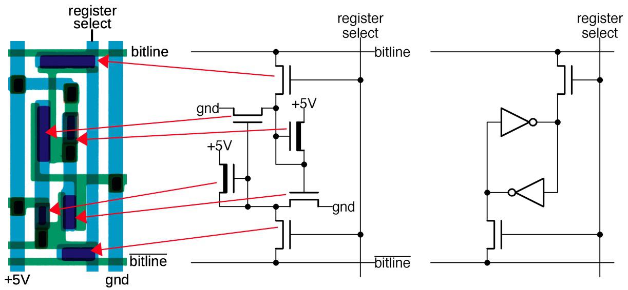
Storing one bit in Nanoprocessor. Each bit is implemented on 6 transistors (6T SRAM cell).
A register set consists of a matrix of such bit cells. The register select bus selects one register (one column) for reading or writing. The upper and lower pass transistors then connect the inverters to their respective horizontal bit lines. For reading, the upper bit line provides the value stored in the cell; there are eight bit lines for the eight bits stored in the register. For writing, the value is transferred to the upper bit line and the inverted value is transferred to the lower one. These values replace the signals of the inverters, causing them to take the desired value and store this bit. Thus, a grid of horizontal bit lines and vertical select lines allows a value to be read or written to a particular register.
Decoding commands
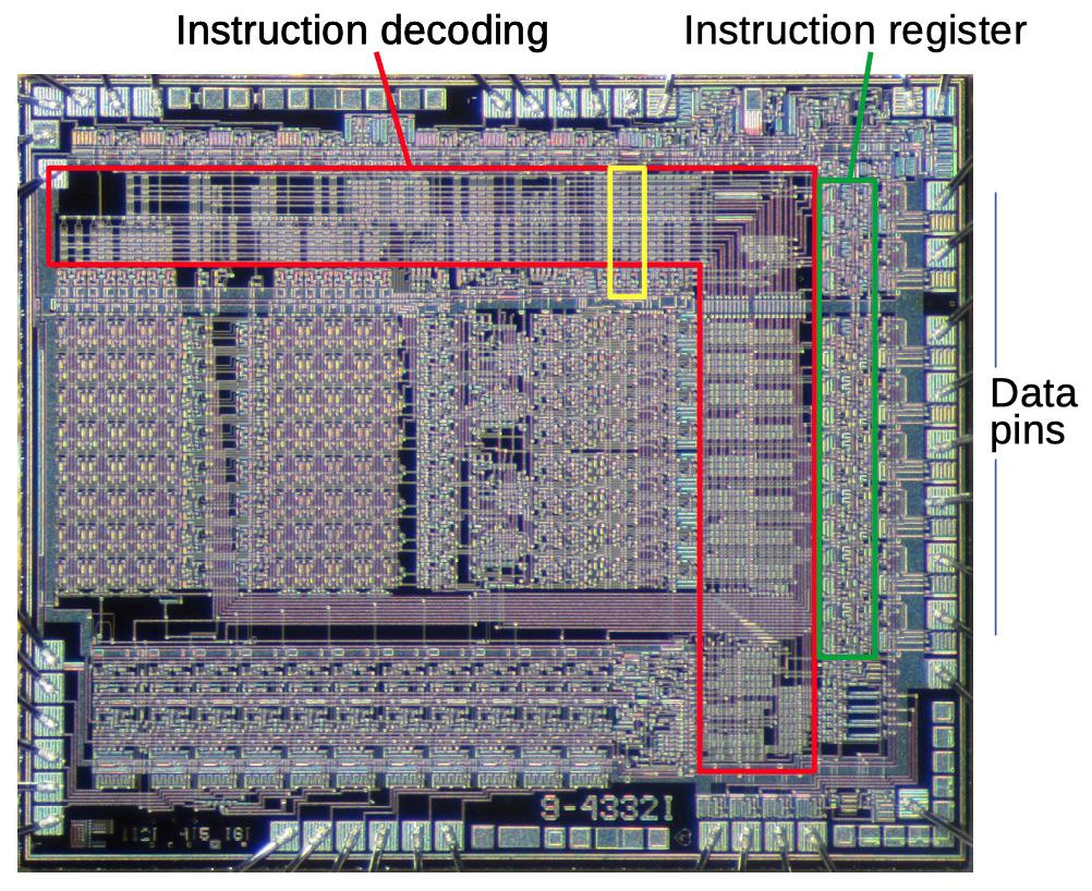
The decoding circuits are engaged in taking the binary code of the instruction (for example, 01101010), and determining what the instruction is (in this case, "load accumulator from register 10"). Compared to many processors, Nanoprocessor's instructions are quite simple: it has relatively few (48), and the instruction code is always one byte. The diagram below shows that the instruction decoding logic (red) takes up a significant portion of the chip. The instruction register (green) is a set of eight latches that hold the current instruction. The command register is located next to the data pins, to which the command comes from the ROM. In this section, we will break down the decoding chain shown in yellow.
Decoding is done by NOR gates. Each NOR gate recognizes a specific command or group of commands. The NOR gate accepts command bits or their complement as input. When all incoming bits are zero, the NOR gate reports a match. This allows you to search for matches both in the whole team as a whole, and in part of the team. For example, the command "load accumulator from register R" has a binary format 0110rrrr, in which the last four bits indicate the required register. The NOR gate (bit7 + bit6 '+ bit5' + bit4) 'will match this command.
An instruction decoder structured in this way is good in that it can be assembled from compact and repetitive circuits. It is often called PLM (Programmable Logic Array). The idea is that the incoming signals to the matrix are fed horizontally, and the outgoing ones are fed vertically. At each intersection there can be a transistor, and then the input signal is part of the gate; if there is no transistor, this input is ignored. The result is compactly arranged NOR valves. In early microprocessors, the decoder was often made from a matrix of NOR gates - for example, this was the case with the 6502.
The diagram below shows three enlarged decoders on the right side, which are circled in yellow in the diagram above. This diagram corresponds to the leftmost decoder. Pay attention to the correspondence of the transistors on the diagram to the pink spots of the transistors on the layout. The idea is that if any input signal activates the transistor, then the transistor pulls the output signal to ground. Otherwise, the output is pulled up by a resistor. The inverters on the bottom amplify the signal so that there is enough current to power all eight parts of the battery. Interestingly, this layout uses pairs of transistors with ground and output connected - I don't see any advantage over just using a single transistor. In any case, notice how the PLM provides a dense arrangement of decoders.
Note that the inverter in the instruction decoder is pulled up to 12 V, not 5 V. This is because the Nanoprocessor uses metal gate transistors instead of the more advanced silicon gate transistors found in other microprocessors of the era. The disadvantage of a transistor with a metal gate is an increased threshold voltage, so the output voltage of the transistor is much lower than the voltage at the gate. The output from a conventional inverter is too small to feed the gate of the pass-through transistor, since its output voltage will drop again. The solution is to use a 12 V power supply for the inverters of the decoder that controls the battery pass-through transistors. Then the signals will have enough voltage to activate the pass-through transistors. In other words, Nanoprocessor needs additional 12+ V,as it uses metal-gate transistors instead of the more advanced silicon-gate transistors.

One of the Nanoprocessor decoder circuits. The diagram on the left corresponds to the left-most decoder of the three shown on the right.
This circuit generates an increment / decrement signal which is fed into the accumulator circuit. The rung detects a match when the signal level of the clock, request, 6th command bit and 2nd command bit is low - a match is found as x0xxx0xx during the execution phase. These commands include “Increment Binary” (00000000), “Increment BCD” (00000010), “Decrement Binary” (00000001), and “Decrement BCD” (00000011).
The chain shown in the diagram looks for matches with commands of the form x0xxx0xx, so the match is found with many more commands than just increment and decrement. Why is it not looking for a complete match? The reason is that if the accumulator is not in use, the activation of the increment / decrement signal is irrelevant. By expanding the list of matching options, the developers could get rid of some of the transistors in the circuit. It is important that the chain overrides other battery-related instructions like "Clear accumulator" (00000100) or "Load accumulator from register" (0110rrrr).
Comparator
An important Nanoprocessor circuit is a comparator that compares the value stored in the accumulator with the value from the R0 register. The comparator uses a single but tricky circuit to compare them. Essentially, the algorithm compares two numbers starting with the most significant bits. If the bits are equal, continue to the lower ones. The first bit difference determines which value is greater (for example, in the case of 10101010 and 10100111, this determines the 4th bit from the right).
The algorithm is implemented in eight steps, one step at a time, starting with the most significant bit at the bottom. Each step consists of two symmetric parts - one determines whether the inequality A> R0 holds, and its additional part checks the inequality A <R0. If the numbers were still equal, but a difference was found at this stage, the stage generates a signal "more" or "less". Otherwise, it passes the decision to a lower level. The final decision is made by the topmost rung. Please note that the comparison for equality in the comparator takes place "for free" - if there are no signals "more" or "less" at the output, then the values are equal.
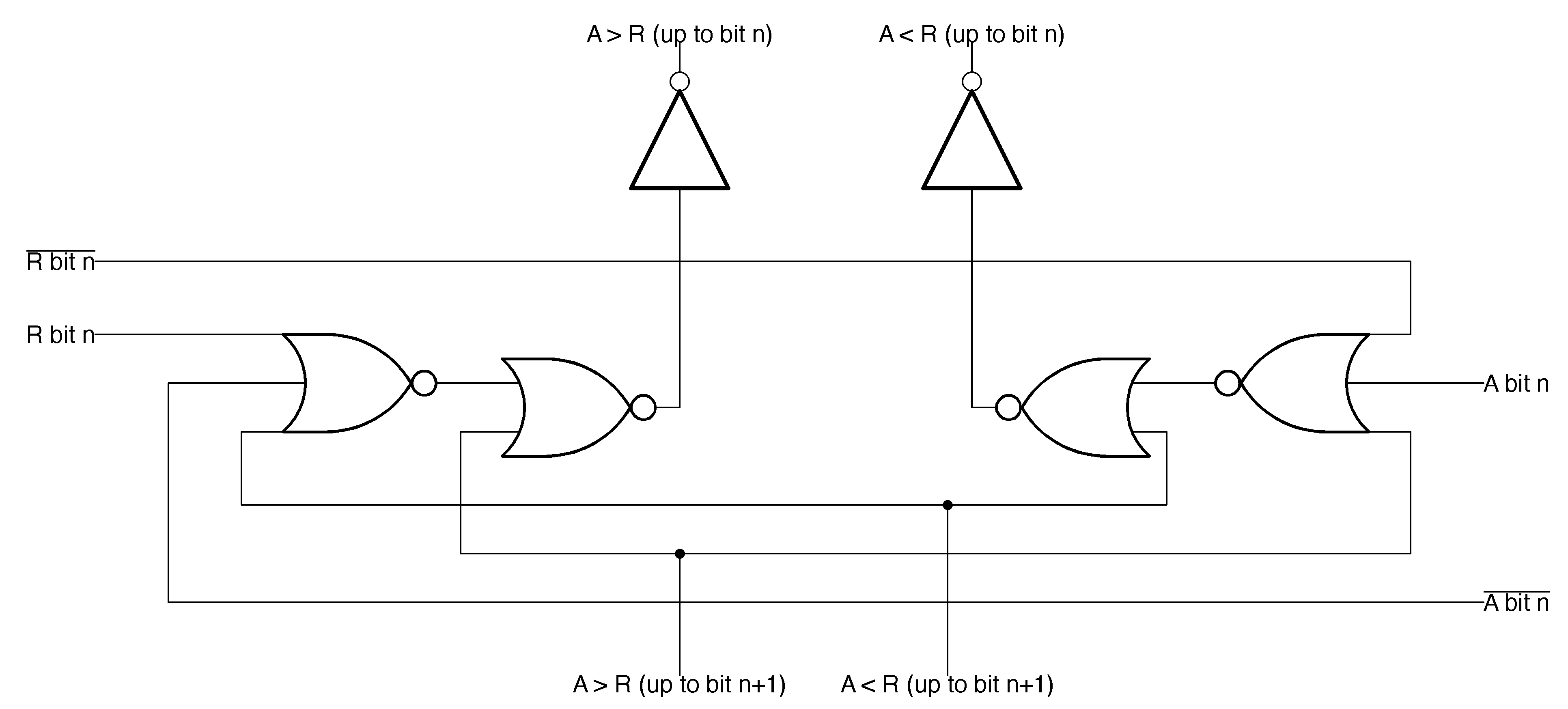
One of the stages of an 8-bit comparator
The diagram below shows the physical layout of the two stages of the comparator. One trick in the comparator layout is that it sits between register 0 on the left and the accumulator on the right, which minimizes the length of the wires. The comparator accesses register 0 directly, bypassing the usual register and data bus selection path.

Two stages of the comparator - as it is specified on the photomask
Nanoprocessor conditional branching commands can inspect the comparator output. Conditional branch circuits are fairly simple: a few bits of the branch instruction select a particular check through the multiplexer. Then the 7th bit of the command decides whether to select "this branch if true" or "this branch if false". Unlike most processors, Nanoprocessor does not allow branching to any address. It simply skips two command bytes if the condition is satisfied (and usually these two bytes contain the command to go to the desired target, but sometimes there are other commands). The skipping scheme is simple: the program counter is called again, while increasing the value not by 1, but by 2, skipping two commands. It turns out that Nanoprocessor implements a wide range of conditional checks on a relatively small number of nets.
Nanoprocessor has a large set of branching conditions - surprisingly large for such a simple processor. You can check the following conditions: A> R0, A> = R0, A <R0, A <= R0, A == R0, or A! = R0. In addition, conditional branching can depend on whether the value in the accumulator is zero or not, whether a particular bit of the value stored in the accumulator is equal to zero, whether the overflow flag is set, or whether a certain bit of the I / O register is set.
Battery and control logic device
The accumulator is a special 8-bit register that stores the byte being processed at the moment. Operations with the battery are carried out by a control logic device (ULU), which is called the "heart of the Nanoprocessor" in the instructions for the processor. ULU is the equivalent of an arithmetic logic unit (ALU) in most processors, only it does not perform arithmetic or logical operations. At the same time, ULU is not as useless as it seems at first glance. It can increment or decrement the value in the accumulator, either in binary or in binary-coded decimal (BCD). The BCD stores two decimal places in one byte. This is a very useful mode for I / O or displays. Also, the ULU can find the binary's complement of the accumulator or reset it, as well as set and clear a certain bit. Finally,it supports left and right shift operations.

Battery related circuits
The diagram above shows the battery and ULD circuits. In the first section, various nets are located, defining a zero value, supporting BCD, and providing carry slip - fast generation of a carry from the least significant 4 bits. The second section contains the main battery and ULU circuits. The third section distributes control signals from the decoding logic above to the eight parts of the accumulator. The last section contains the instruction decoding logic that decodes the bit operations and sends the signal to the desired part of the accumulator.
The main body of the accumulator / ULU consists of 8 parts, one per bit, with the least significant bit at the top. We'll look at four circuits from each part: a carry generator for increment / decrement operations, a bit generator for increment / decrement operations, a multiplexer for selecting a new accumulator value, and a latch where the accumulator value is stored.
Each part of the increment / decrement device (below) is implemented using a half adder. The direction of the increment / decrement chain determines the opcode: 0 in the low-order bit of the opcode says increment and 1 for decrement. The carry chain on the left generates the carry signal. For an increment, create a carry output if a carry input is received and the current bit is 1 (since then it will be incremented to binary 10). For decrement, the carry line signals a borrow , so a carry output is generated when there is a carry input (i.e., borrow) and the current bit is 0.

One piece of the increment / decrement chain
The rung to the right updates the current bit with an increment or decrement. The current bit is toggled when a carry input is present - essentially an XOR implementation through three NOR gates. One of the difficulties is adjusting for BCD. For the BCD increment operation, the carry occurs when the digit 9 is incremented, and for the BCD decrement operation, the digit 0 decreases to 9 instead of binary 1111.
The multiplexer manages the various battery operations. Depending on the operation, one pass transistor is activated, selecting the desired value. For example, for an increment / decrement operation, the upper transistor selects the output from the increment / decrement circuit described above. The transistor activates the previously described instruction decoder, which has found the corresponding increment / decrement instruction. Likewise, a right shift command activates the right shift transistor by applying n + 1 battery bits to each of the accumulator parts to shift the value.

Circuitry for a latch that stores one bit of the battery and a multiplexer that selects the input for the battery
The latch stores one bit for the accumulator. When the battery hold transistor is activated, the two NOR gates form a holding loop. If the battery load transistor is activated instead, the battery loads the desired value from the multiplexer. The lines to clear the n bit and set the n bit allow commands to change individual bits of the accumulator; the multiplexer then updates all bits of the accumulator at once.
Counter and program addressing
Another large block of chains is the 11-bit program counter located in the lower left corner of the Nanoprocessor. Also in this block there is a latch that stores the return address from the subroutine, and another latch that stores the program counter after interruption. Think of them as a stack of one element long. The software counter has an increment device that is responsible for moving to the next command. It also knows how to increment by two at once, allowing conditional branch instructions to skip two instructions (such an increment device is implemented simply by increasing the 1st bit instead of the 0th bit). To speed up the operation of the increment device, it has a carry-over function; if all six least significant bits are 1, it will increment the 6th bit at once, without waiting for the carry to go through all the least significant bits.
Control and clock frequency
The last part of Nanoprocessor is the control circuit. Compared to other microprocessors, the Nanoprocessor control scheme seems almost trivial: the processor goes from request clock to execution clock and back (with periodic interrupts). The control circuit is just a couple of flip-flops and gates, so there isn't much to say about it.
Conclusion
The diagram below shows the main functional blocks of Nanoprocessor. Nanoprocessor managed to fit them very tightly, much better than I would expect from the outdated metal shutter technology. Reverse engineering shows that these functional blocks are implemented with simple but carefully designed circuits.
Nanoprocessor used metal gate transistors, while other microprocessors have started to switch to silicon gate transistors for several years. The difference may seem incomprehensible, but it has a significant effect on the location of the components: in the manufacture of a transistor with silicon gates, a layer of polysilicon with conductors is added. As a result, component placement becomes much easier, since you have two layers with conductors at your disposal, capable of passing through the adjacent layer. If you only have a metal layer, it is much more difficult to position the components because the conductors get in the way. In other chips I have studied that used metal gate transistor technology,the layout of the components was disgusting - a bunch of tangled wires bringing signals to each transistor kept the density of the transistors low. On the other hand, the Nanoprocessor function blocks are very carefully designed and all signals get along just fine. There is a bit of extra space, for example, for the data bus, but overall I'm impressed with the density of the Nanoprocessor layout.
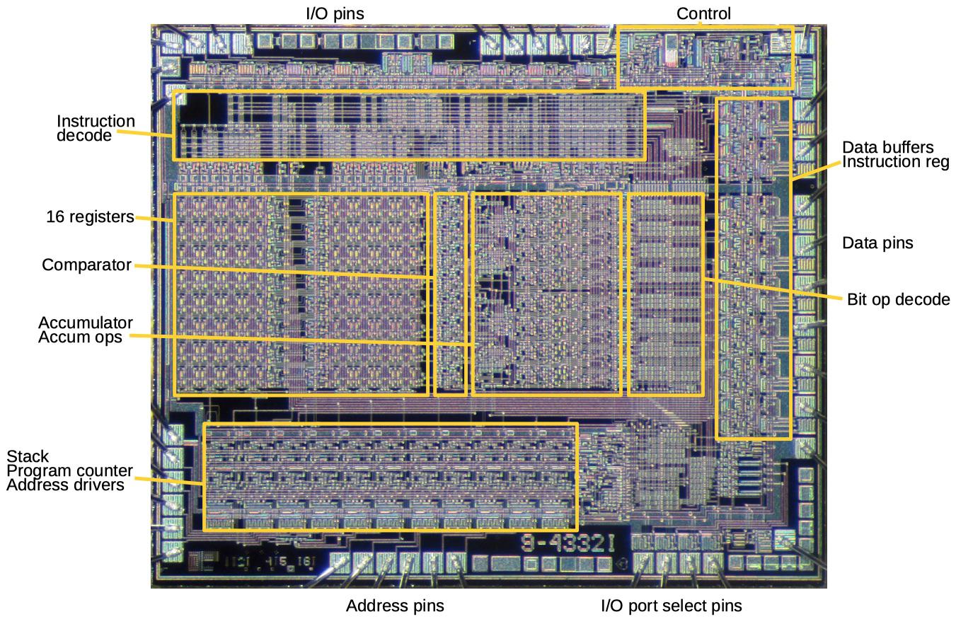
Nanoprocessor functional components based on my reverse engineering
Nanoprocessor - the processor is unusual. At first glance, it even seemed to me to be a "fake processor", due to the lack of basic arithmetic operations. However, after studying it in more detail, I was still impressed. Its simple design allows it to run faster than other processors of the time. The command set can do more than meets the eye. Hewlett-Packard used Nanoprocessor in many of its products in the 1970s and 1980s, in more complex roles than might be expected — for example, parsing strings and performing computations. After his masks have been published, we can learn all the secrets of the chains thanks to which Nanoprocessor worked.
Nanoprocessor (white chip) as part of the Hewlett-Packard precision timing module. Note the handwritten voltage; each chip required its own bias voltage.