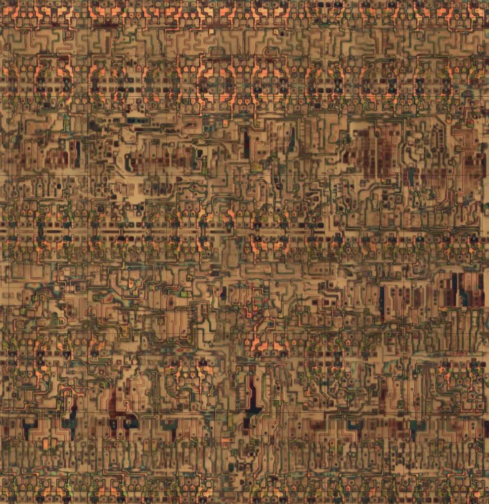
The photo shows one of 64 blocks of the XC2064 chip. The metallization layers are removed, we can see silicon and polysilicon transistors lying under the metallization. You can see a larger scale photo here: siliconpr0n .
The FPGA was invented by Ross Freeman, co-founder of Xilinx in 1984, the first FPGA was the XC2064. It was much simpler than modern FPGAs, contained only 64 logic blocks, compared to the thousands and millions in modern FPGAs, and its creation led to the emergence of an industry worth billions of dollars. The XC2064 is so important that it entered the Chip Hall of Fame. I have reverse engineered the XC2064 and in this post I explain its internal structure in general terms and how it is programmed with a bitstream.
Ross Freeman
(Ross Freeman) 45 , . 2009 , .
Xilinx
Xilinx -. , , Xilinx , . Xilinx Seiko Epson Semiconductor Division ( Seiko Epson).
XC2064
: ( ) . — (Programmable Logic Devices, PLD), , , 1967 . , , , . , PROM, , , EPROM, . , , Programmable Logic Array, Programmable Array Logic (1978), Generic Array Logic Uncommitted Logic Array. , , « », . , , , , , . , . "Three Ages of FPGAs: A Retrospective on the First Thirty Years of FPGA Technology." "A Brief History of FPGAs".

Xilinx XC2064 is the first FPGA chip. Taken from here: siliconpr0n .
FPGAs are currently programmed in hardware description languages such as Verilog or VHDL, but at the time, Xilinx provided its own development software, an MS-DOS application called XACT, for the hefty $ 12,000. XACT worked at a lower level than modern tools: the user defined the function of each logical block, as shown in the screenshot below, and the connections between the logical blocks.
XACT routed the connections and generated a configuration file (bitstream) that was loaded into the FPGA.
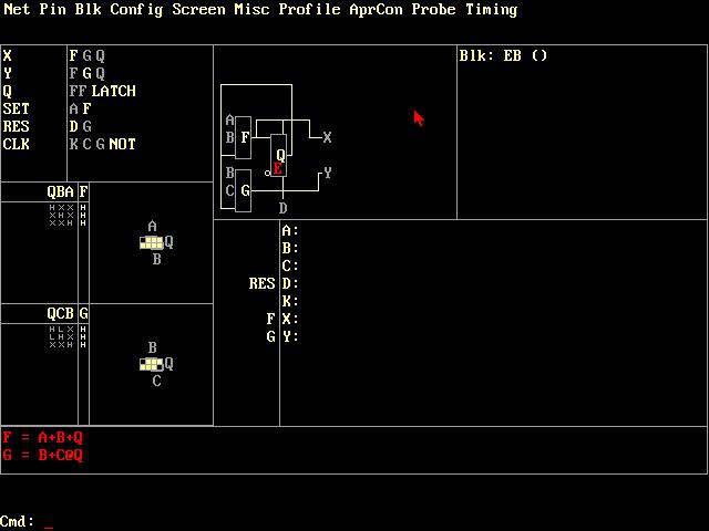
Screenshot of XACT. The two tables F and G implement the equations shown at the bottom of the screen, with the Karnaugh map shown above.
The FPGA was configured using a bitstream, a sequence of bits in a proprietary format. If you look at the XC2064 bitstream (below), you will see a mysterious mixture of patterns that repeat themselves in an irregular manner and are scattered throughout the bitstream. However, studying the physical circuits of FPGAs reveals the data structure of the bitstream and it can be studied.

Part of the bitstream generated by XACT.
How does FPGA work?
The figure below, taken from the original FPGA patent, shows the basic structure of an FPGA. This simplified FPGA has a total of 9 logic blocks (marked in blue), and 12 I / O ports. An interconnect network connects components together. By setting switches (diagonal lines) on the connections, logic blocks can be connected to each other and to the I / O ports. Each logic element can be programmed for the required logic function. As a result, such a programmable chip can implement any device that fits into the available space.
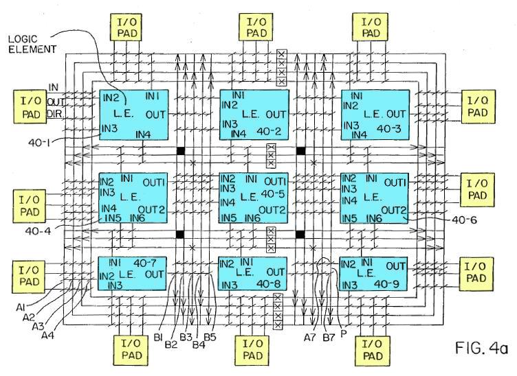
FPGA patent , logical blocks (LE) interconnected.
Configurable Logic Block (CLB)
Although the picture above shows 9 CLBs, the XC2064 has 64 CLBs. The figure below shows the structure of the CLB. CLB has 4 inputs (A, B, C, D) and two outputs (X and Y). In between is combinational logic, which can be programmed to any desired logic function. The CLB also contains a trigger, the presence of which allows you to implement counters, shift registers, state machines and other stateful circuits. Trapeziums indicate multiplexers that can be programmed to pass a signal from any of the inputs. Multiplexers allow you to configure the CLB for a specific task by selecting specific signals to control the trigger and outputs.

Configurable logic block in XC2064, taken from here: datasheet .
You might be wondering how combinational logic implements arbitrary logic functions. Is there a choice between a set of AND, OR, XOR, and so on? No, there is a clever trick called the lookup table (LUT), which is actually the truth table for the function. For example, a function of three variables is defined by a table of 8 rows. The LUT contains 8 bits of memory. We can implement any 3-input logic function while keeping those three bits.
View tables
XC2064 — , . CLB . XC2064 , 4 . , .

XC2064 . .
XC2064 . .
Connections
The next key aspect of FPGAs is the connections, which can be programmed to switch the CLB in a variety of ways. The connections are complex, but the rough description is that there are segments of vertical and horizontal connections between all CLBs. You can connect CLB with horizontal and vertical lines, and create arbitrary connections. A more complex type of connection is the "switch matrix". Each matrix has 8 pins that can be connected to each other (almost) in any way.
The figure below shows the structure of the XC2064 links that provide connections between logic blocks (blue) and I / O lines (yellow). The inset shows the details of the coupling mechanism. The green rectangles are 8-pin switch matrices and the small squares are the programmable connection points.
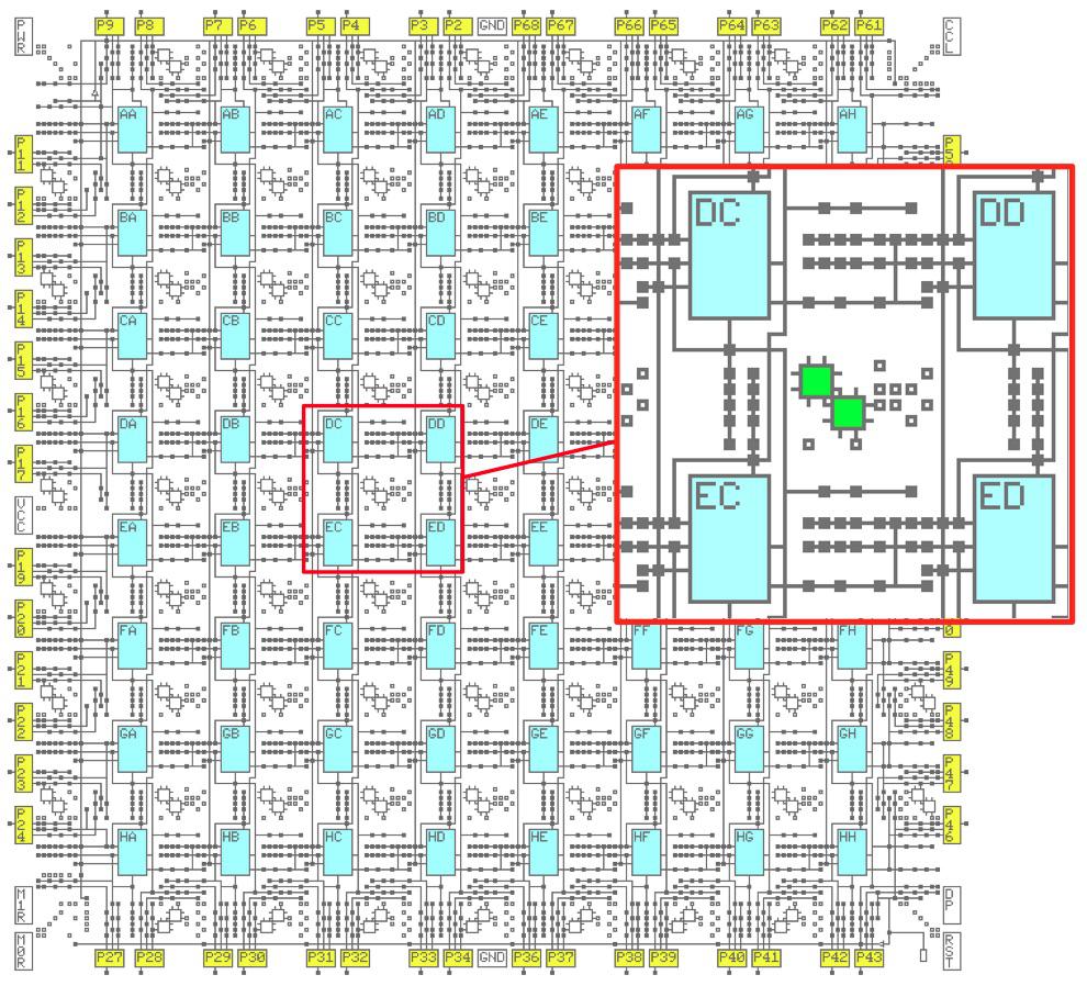
The XC2064 FPGA has an 8x8 CLB matrix. Each CLB has a name from AA to HH.
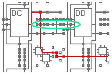
The connection can switch, for example, the output of a DC block to an input of a DE block, as shown below. The red line shows the signal path and the small red squares show the activated connection points. Coming out of the DC block, the signal is routed to the first connection point on an 8-pin switch (green), which routes it through two connection points and another 8-way switch (unused vertical and horizontal lines not shown). Note that the connection is quite complex, even such a short path uses four connection points and two switches.
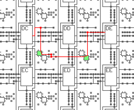
Example of signal routing from the output of a DC block to a DE block.
The screenshot below shows how tracing is done in XACT. Yellow lines show connections between logical blocks. As the number of signals increases, it becomes difficult to make connections without conflict between paths. XACT automatically traces, but the trace can also be manually edited.
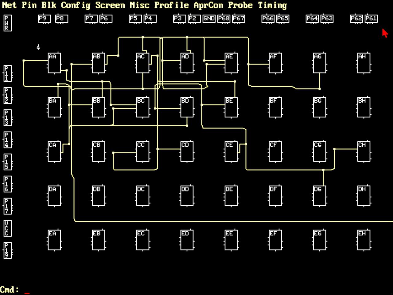
Screenshot of XACT program. It is an MS-DOS program and is controlled by keyboard and mouse.
Implementation
Next, we'll look at the internal circuitry of the XC2064 by reverse engineering from a photo of the crystal. Be warned that this requires some familiarity with the XC2064.
Crystal photo
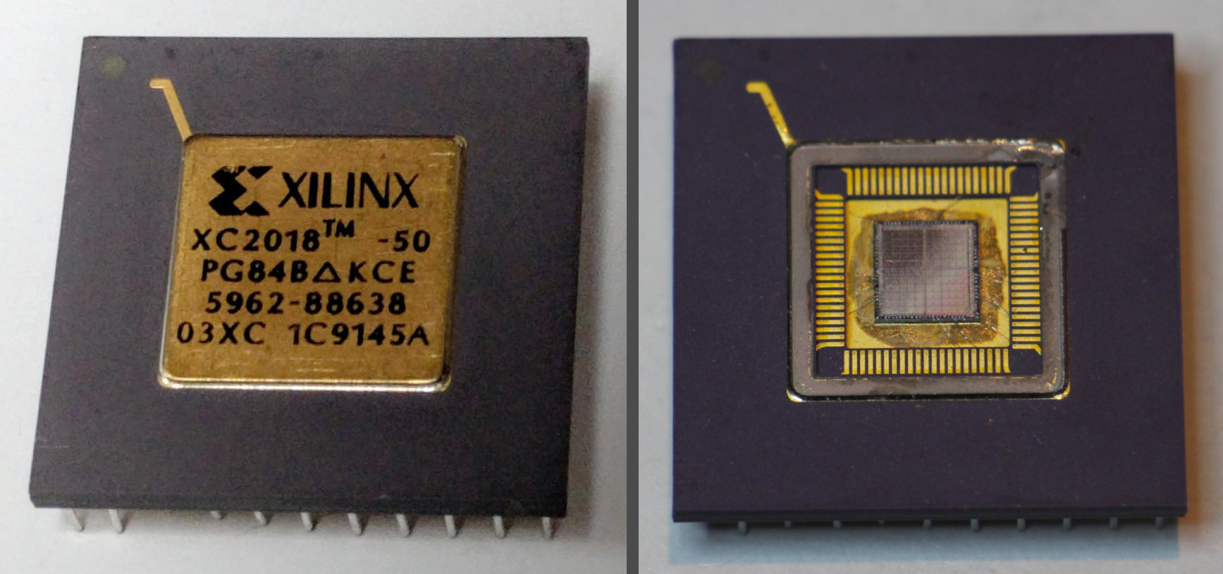
XC2064 XC20186, XC2064 XC2018 siliconpr0n. , . John McMaster , , . , .
XC2064 , John McMaster.
XC2064 , John McMaster.
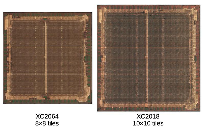
XC2018
Xilinx XC2018 ( ) 100 , , XC2064. , XC2064 64 , 1010, 88. XC2018 , .
XC2018. , . .
XC2064 XC2018. , , .
XC2064 XC2018. , , , . siliconpr0n.
XC2018. , . .
XC2064 XC2018. , , .
XC2064 XC2018. , , , . siliconpr0n.
Below is a photo of the XC2064 crystal. The main part of the FPGA is a matrix of 8x8 blocks, each of which contains a logic block and surrounding circuits. Although the FPGA diagram shows logical blocks (CLBs) as separate from the entity wiring diagrams, in reality this is not the case. In fact, each logical block and its environment are implemented as a single node, a tile. (To be precise, the tile includes connections at the top and left of each CLB.)
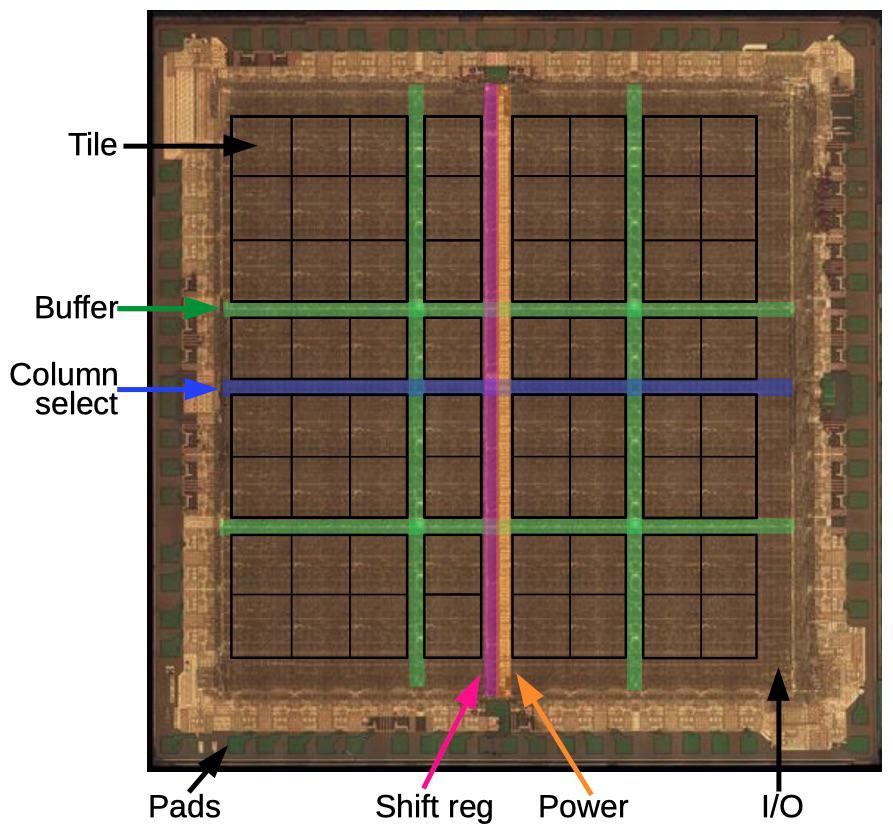
XC2064 block layout. Taken from here: siliconpr0n .
Located along the sides of the integrated circuit, I / O blocks provide communication with the outside world. They are connected to the pins of the crystal, which are shown as small green squares, and connected to the pins of the microcircuit case. There are buffers on the die (green): two vertical and two horizontal. These buffers amplify the signal that travels a long distance across the chip and reduce latency. The vertical shift register (pink) and the horizontal column fetch chain are used to load the bitstream into the chip, as shown below.
Inside the tiles
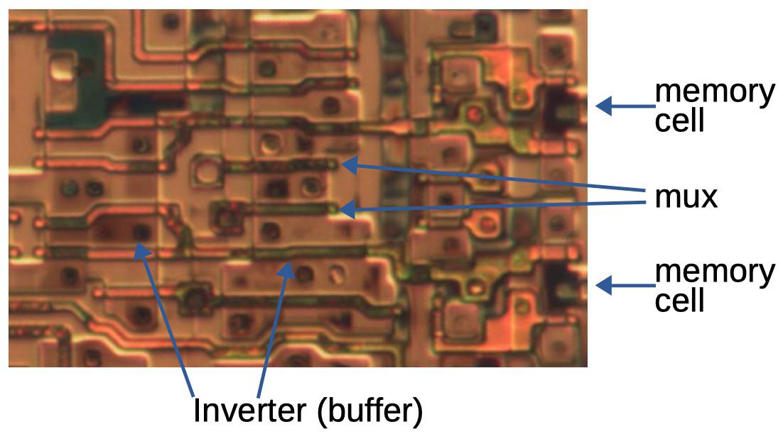
The figure below shows the structure of one XC2064 tile, the chip contains 64 such tiles packed on one die. About 40% of each tile is occupied by memory cells (shown in green) that store configuration bits. The top third (approximately) of the tile contains the connection diagrams: two switch matrices and a number of individual link switches. Below is the logical block. The main part of the logic block is the input multiplexer, flip-flop and lookup table. The tile is connected to neighbors through horizontal and vertical communication lines, and it is also connected to the power and ground rails. The configuration data bits enter the memory cells horizontally, and the vertical signals select a specific column to load.
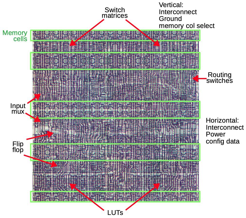
One FPGA tile showing important functional nodes
Transistors
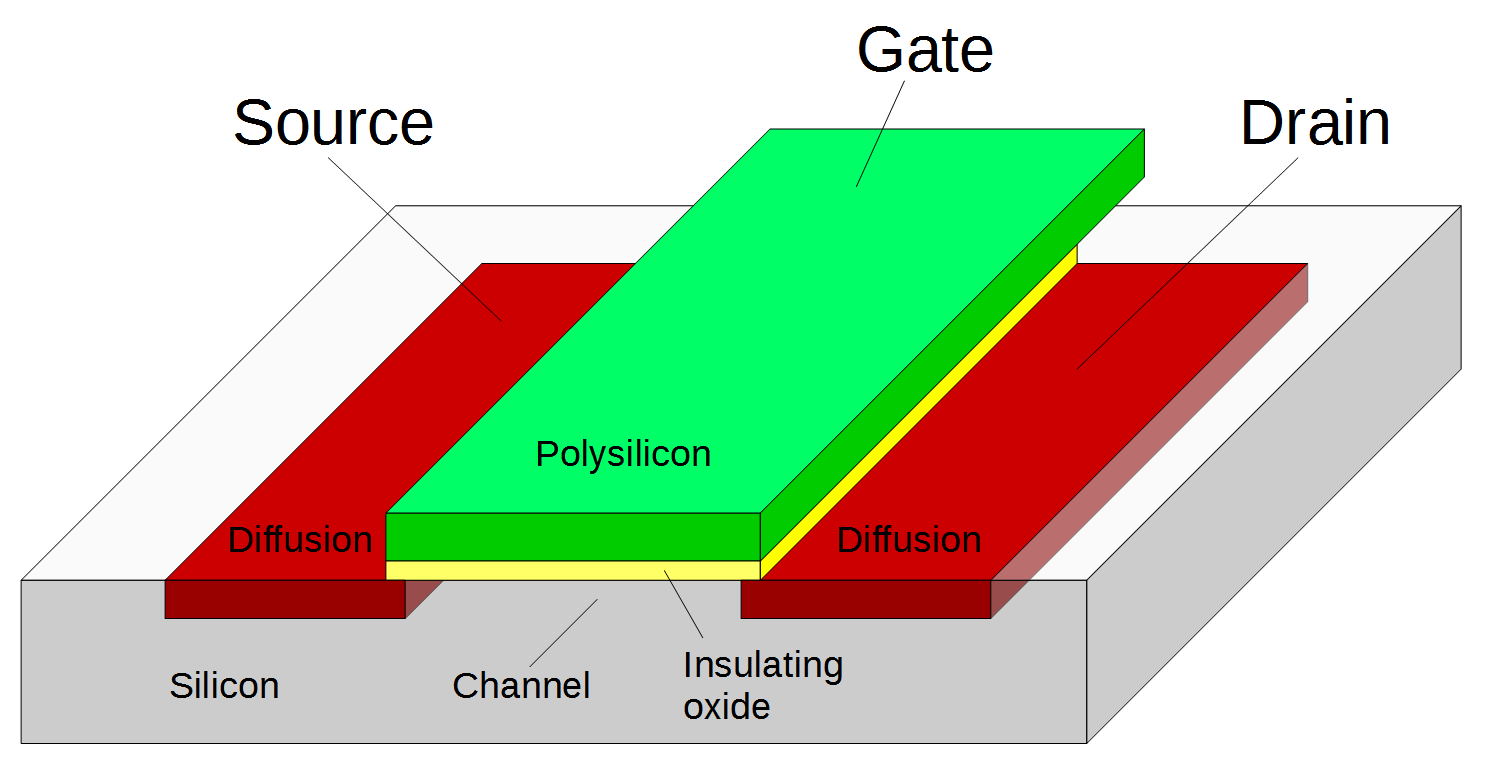
FPGA is implemented on CMOS (CMOS) logic, built from NMOS and PMOS transistors. Transistors play two main roles in FPGAs. First, logical elements are formed from their combinations. Secondly, transistors are used as switches through which a signal passes, for example, to form connections between blocks. A transistor that performs this role is called a through transistor. The figure below shows the basic structure of a MOSFET. Two sections of silicon are doped with impurities to create a drain and a source. Between them is a gate that turns the transistor on and off and controls the current between the drain and source. The shutter is made of a special type of silicon called polysilicon, insulated from the silicon underneath by a thin layer of oxide. Above it, there are two layers of metallization, which provide circuit connections.
MOSFET structure
In the photo of the crystal, we can observe what the transistor looks like under a microscope. The polysilicon gate is a serpentine line between two doped regions of silicon. The circles are vias connecting the silicon and the metal layer (which is removed in this photo).

FPGA MOSFET
Bitstream and configuration memory
The configuration information in the XC2064 is stored in the configuration memory locations. The FPGA does not use block memory for this, instead, the configuration memory is distributed throughout the crystal in the form of a 160x71 grid, each bit is placed next to the circuit that it controls. The figure below shows the configuration bitstream loaded into the FPGA. The bitstream is loaded into the shift register that goes in the middle of the chip (pink). Once 71 bits are loaded into the shift register, the column fetch circuit (blue) selects the desired memory column and the bits are loaded into the column in parallel. Then the next 71 bits are loaded into the shift register and the next column to the left is selected. The process is repeated for all 160 columns of the FPGA, and the entire bitstream is loaded into the FPGA. The use of a shift register eliminates the need for large memory addressing circuits.
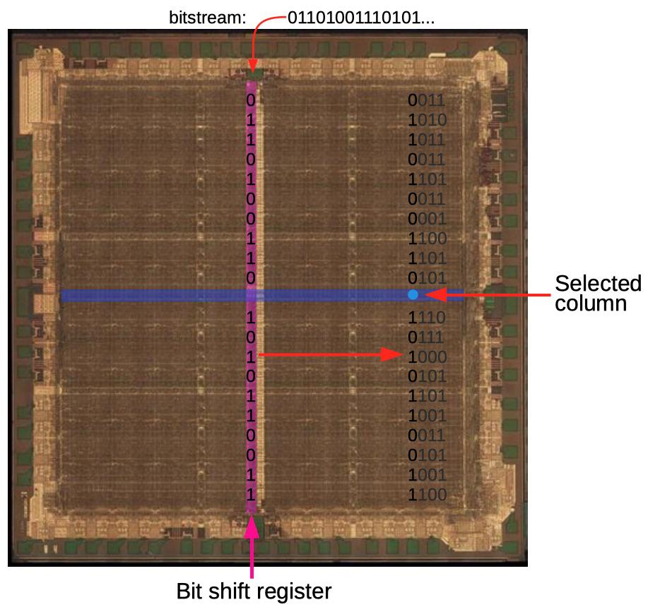
How the bitstream is loaded into the FPGA. Bits are shown conventionally, the actual storage of bits is much denser. The three columns on the right have already been loaded and the fourth is loading. The photo of the crystal is taken from here: siliconpr0n .
The important thing is that the bitstream is distributed across the chip in exactly the order in which the bits appear in the file: the packing of the bits in the bitstream corresponds to their physical placement on the chip. As shown below, each bit is stored in the FPGA next to the circuit it controls. thus, the bitstream file format is directly determined by the placement of the hardware circuits. For example, if there is a gap between tiles, and there is a buffer in it, the same gap will be in the bitstream. The structure of the bitstream does not depend on software abstractions such as fields in data tables or configuration blocks. Understanding bitstream requires thinking in hardware terms, not software
Bitstream
, (.RBT) , .
, .
, .
Each bit of configuration memory is implemented as shown below. Each memory cell consists of two inverters connected in a loop. such a circuit has two stable states, and can store one bit: either the upper inverter is in state 1, and the lower one is in state 0, or vice versa. To write to the cell, the pass transistor on the left is activated, passing the signal. The signal on the data line simply pulls the inverter, writing the required bit. (You can also read the configuration data using the same rung.) Output Q and inverted Q control a specific function in the FPGA, such as closing an interconnect, retrieving a bit from a lookup table, or controlling a trigger. In most cases, only the Q output is used.
SRAM cell
(SRAM). , RAM, , , SRAM. , 5T SRAM.
, . , . , 1818 , 27 . , , , , . 9 .

, , . siliconpr0n.
, . , . , 1818 , 27 . , , , , . 9 .
, , . siliconpr0n.

Diagram of one bit of configuration memory, from the documentation.
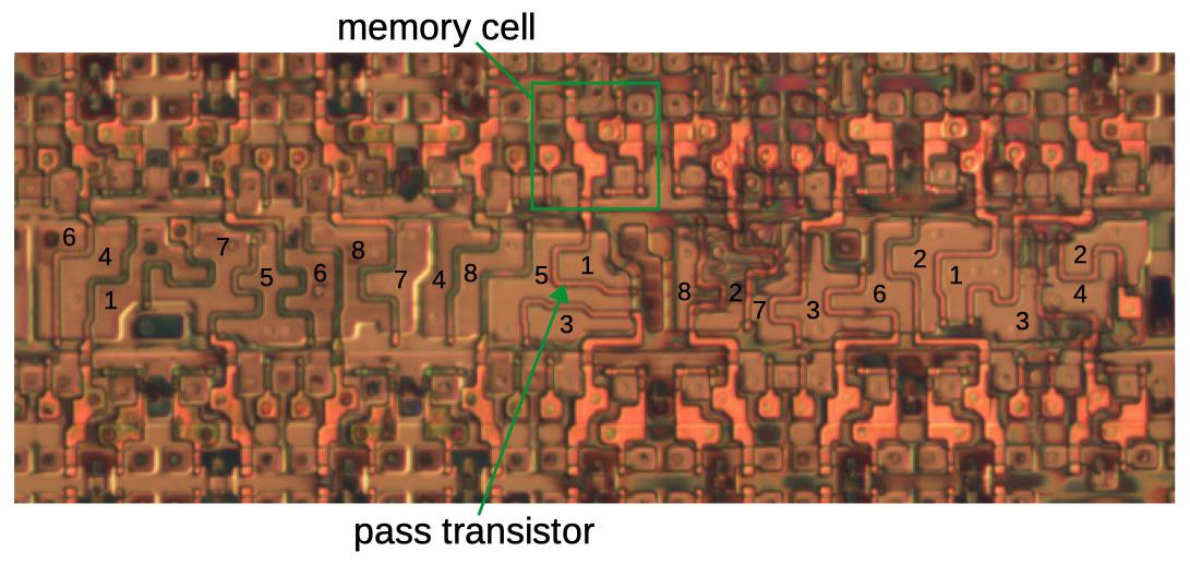
The figure below shows the physical structure of memory cells. The photo on the left shows 8 memory cells, one of which is highlighted. Each horizontal data line is connected to all memory locations in the row. Each column fetch line selects all memory locations in the column, allowing writing. The middle photo shows sections of silicon and polysilicon for one memory cell. The layers of metal have been removed to expose the transistors underneath. Metallization layers connect transistors, circles in the photo, these are connections, vias, between silicon or polysilicon and metal. The diagram shows how five transistors are connected, the placement of the elements on the diagram corresponds to their placement in the photo. Two pairs of transistors form the CMOS inverters, with a pass-through transistor on the bottom left providing access to the cell.
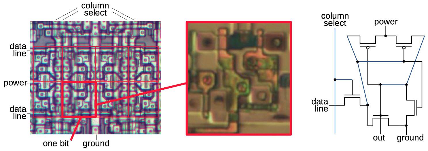
, . — . , . . : siliconpr0n.
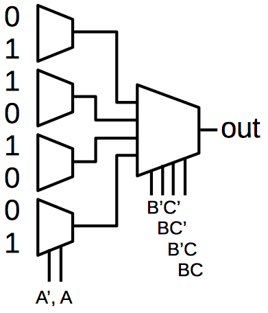
As explained earlier, FPGA implements arbitrary logic functions using lookup tables. The figure below shows how the lookup table is implemented in XC2064. The eight values on the left are stored in eight memory locations. Four multiplexers select one of each pair of values, depending on the value at the input A, if A = 0, the upper of the values is selected, if A = 1, then the lower. Then, the large multiplexer chooses one of four values based on signals B and C. The result will be a specific value, in this case A XOR B XOR C. We can do any logic function if we substitute different values into the table.
XOR implementation in the lookup table.
Each multiplexer is implemented using pass-through transistors. Depending on the control signals, one of the pass-through transistors is activated, passing data from input to output. The figure below shows a portion of the LUT chain, with two bits multiplexed. On the right are two memory locations. Each bit is passed through the inverter, amplified, and passed through the pass-through transistors of the multiplexer in the middle, selecting one of these bits.
View of the nets that implement the LUT. Taken from siliconpr0n.
Trigger
Each CLB contains a flip-flop that allows the FPGA to implement latches, state machines, and other stateful nets. The figure below shows a (somewhat unusual) trigger implementation. She uses the following scheme. When the clock signal is zero, the first multiplexer passes data to the first latch, which stores the value. The bit is inverted twice, as it passes through the OR, NAND and inverter gates, and remains the same as a result. further, the second latch multiplexer receives the bit from the first latch when the clock goes up to 1 (note that the clock is inverted). This value is the output of the flip-flop. When the clock signal is set to 0, the secondary multiplexer closes the loop by latching the bit. Thus, the trigger is sensitive to the edge of the signal,latching the value on the leading edge of the clock signal. Set and reset lines set and reset the flip-flop.
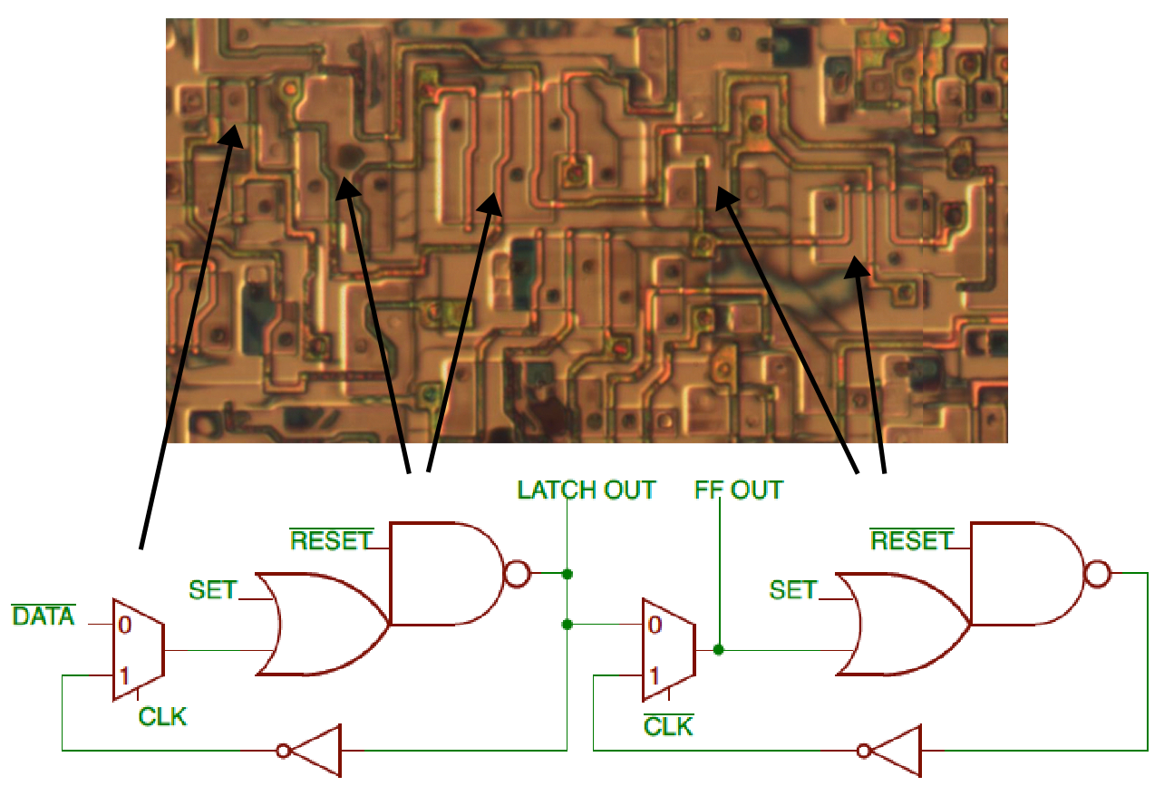
. OR-NAND : siliconpr0n.
The switch matrix is an important interconnection element. Each switch has 8 pins (two on each side) and can connect them in almost any way. Signals can be unwrapped, split, intersected with more flexibility than at individual interconnect nodes. The figure below shows a portion of the interconnect network between the four CLBs (blue). Switching matrices (green) can be connected in any combination of connections on the right side. Note that each pin can be connected to other pins in the amount of 5 to 7 pieces. For example, pin 1 can be connected to pin 3, but not to pins 2 and 4. This makes the matrix almost complete, with 20 possible connections instead of 28.
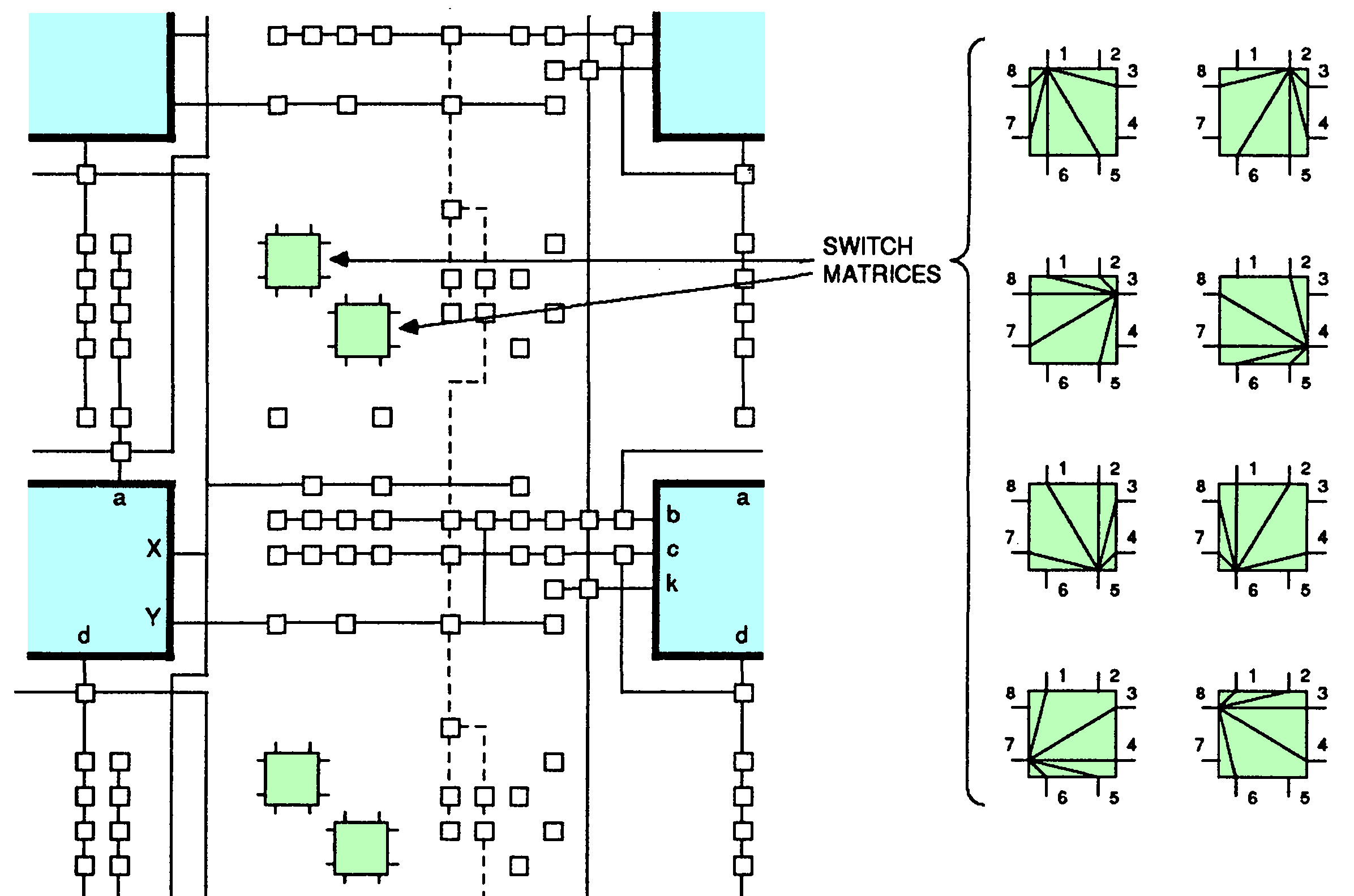
Taken from here: Xilinx Programmable Gate Array Data Book , fig. 7b.
The switching matrix is formed by rows of pass-through transistors controlled by the memory cells above and below them. The two sides of the transistor are two pins of the switching matrix that can be connected by the transistor. So each matrix has 20 control bits, two matrices per tile gives us 40 bits per tile. The photo below shows one memory cell connected to the wavy gate of the pass transistor below it. This transistor provides the connection between pin 5 and pin 1. Thus, the bit in the bitstream corresponding to this memory location controls the connection between pins 5 and 1. Similarly, other memory cells and their associated transistors control other connections. Note also that the order of these connections does not follow any particular pattern, as a result,the correspondence between the bits in the bitstream and the switch pins looks random.
Switch Matrix
20 . 18 , .
Implementation of an 8-lead matrix of connections. The silicon regions are designated by the numbers of their corresponding pins. The metal layers that connected the corresponding leads to the transistors have been removed. Taken from siliconpr0n.
Input connections
CLB inputs use a different bitstream encoding scheme, which is explained by its hardware implementation. In the image below, the eight ellipsed nodes are potential inputs to the CLB called DD. Only one node (maximum) can be configured as an input, since connecting two signals to one input can short them together.
Input selection. The eight inputs circled in green are potential DD inputs, only one of them can be selected.
The required input is selected by the multiplexer. A straightforward solution would be to use an 8-input multiplexer with three control bits choosing one of 8 signals. Another straightforward solution would be to use 8 pass transistors, each with its own control signal, one of which selects the required signal. However, the FPGA uses a hybrid approach that eliminates the need for a decoder in the first case, but requires 5 control signals instead of the 8 required in the second approach.
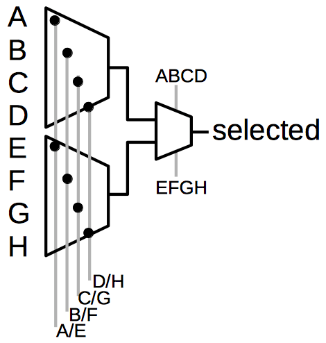
The FPGA uses multiplexers to select one of eight inputs.
The diagram in the figure above shows the two-layer multiplexer used in the FPGA. At the first stage, one of the control signals is activated. In the second stage, the high or low signal is selected and applied to the output. For example, suppose the control signal B / F is applied to the first stage, and ABCD to the second stage, input B will be the only one that goes to the output. That is, selecting one of the eight inputs requires 5 bits in the bitstream and uses 5 memory locations.
Input multiplexer CLB
CLB. EFGH ABCD, . -, CLB 6 10 , , . , , , , . , , 6 , . , , .
Conclusion
The XC2064 uses a variety of highly optimized nets to implement logic blocks and net interconnection. These chains need to be tightly packed in order to fit into the crystal. Even so, the XC2064 was a very large chip, larger than the microprocessor at the time, and was difficult to manufacture, costing hundreds of dollars. Compared to modern FPGAs, the XC2064 has an absurdly small number of cells, but even that was the start of a revolutionary new product line.
Two concepts are key to understanding the XC2064 bitstream. First, the FPGA is implemented on the basis of 64 tiles, repeating blocks that combine logical blocks and interconnects. Although the FPGA is described as having logical blocks surrounded by interconnects, it is not implemented that way. The second concept is that the bitstream is not based on any abstractions, it directly maps the two-dimensional packing of FPGA memory cells. Thus, bitstream only makes sense if you are considering the physical structure of the FPGA.
Note
, XC2064 (. 11), CLB . , , 20% , . — -, . , . .
, 8×18. , , . .

. , #1 () #2 () . 8 #1 1 8 . #2 , . , "#2: 1-3" , 1 3 #2. «ND», , . ND ND.
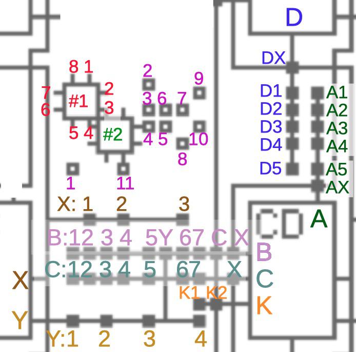
, . , PIP , , . () (1, 2, 3), Y (). (-) -. , , . (), D (), A () . CLB, . , . X Y (LUT) F G. LUT. LUT F LUT G, . , 8 LUT , .
, 8×18. , , . .
. , #1 () #2 () . 8 #1 1 8 . #2 , . , "#2: 1-3" , 1 3 #2. «ND», , . ND ND.
, . , PIP , , . () (1, 2, 3), Y (). (-) -. , , . (), D (), A () . CLB, . , . X Y (LUT) F G. LUT. LUT F LUT G, . , 8 LUT , .
I have announced my last post on twitter, so follow kenshirriff . I also have an RSS feed . Thanks to John McMaster, Tim Ansell and Philip Freidin for the discussions.
Patents
: 4870302, 4642487, 4706216, 4758985, RE34363. XACT Xilinx, , , . . (John McMaster) xc2064.