Intel / Micron NAND Flash Chip
Non-Volatile Memory (NVM) devices are electronic read and write storage devices that continue to store information after a power failure. These include devices based on magnetic disks and certain types of semiconductor chips. Semiconductor non-volatile devices play an important role in all aspects of the digital universe - from the storage cells of huge data banks in the cloud to portable personal devices - and constitute one of the largest segments of the $ 400 billion semiconductor industry.
Like any important semiconductor product, from transistor to microprocessor, NVM devices have come a long way from the work of early explorers who took the work of their predecessors as a basis and developed them through inspiration, luck, trial and error, as well as a determination to ignore the doubts of skeptics. In this article, we share chronologically some of these pioneers and their contributions, from the early beginnings of an idea in 1960 at Fairchild to the large-scale production of flash chips in the last decade of the 20th century.
On behalf of the Semiconductor Special Interest Group (SIG), Jeff Katz recorded interviews with contributors to the development of commercial NVM semiconductor devices for the Oral History CollectionMuseum of Computer History. Many of the personal comments cited below are taken from interview transcripts, which can be accessed through the links in the text.
Before semiconductor non-volatile memory
Before the advent of semiconductor devices, the most successful technology for nonvolatile computer storage was magnetic core memory, which used the effect of magnetic hysteresis. In his dissertation1952 for his MIT Ph.D. Dudley Buck described ferroelectric crystals that used a similar hysteresis mechanism to store and magnetize digital information. Reid Anderson and Walter Merz of Bell Telephone Laboratories demonstrated in 1955 the ferromagnetic storage device that was the forerunner of the NVM semiconductor architecture. Using deposition and etching technologies, they fabricated a 256-bit array of crystals connected by metal paths; later, such technologies began to be applied to the production of semiconductor integrated circuits.
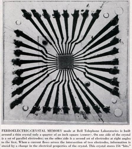
Photo from Scientific American magazine , June 1955.
Colorado Springs-based Ramtron founders Larry McMillan and George Rohr pioneered the commercialization of Ferroelectric Random Access Memory (FRAM) devices , first introduced in 1952.
Evolution of NVM Cell Technology - The First Four Decades
In the 1960s, research began on the two main technologies for designing semiconductor NVM cells. In a “floating gate” cell, the charge is stored on an electrode that is not connected to an external circuit. "Charge trapping", most often called "nitride trapping", allows charge to be stored in a layer of silicon nitride connected to an active circuit. Both technologies promised significant benefits and reduced manufacturing costs, ease of use, and data retention for a variety of applications.
Commercial components and systems using both technologies began to emerge in the 1970s. Products based on charge capture were most often called EAROM (Electrically Erasable Read Only Memory), and the first floating gate devices were called EPROM (Erasable Programmable ROM).
By the 1980s, floating shutter memory had become the dominant technology in the market. EPROMs and their enhancements, including the first flash products, have become a significant percentage of the global semiconductor industry's profits. In the 1990s, Flash technology provided new opportunities for NVM devices, and they began to be used in solid state drives and consumer digital devices.
1960s - pioneers of the memory element
Sa Zhitan, circa 1989
Sa Zhitan of the Fairchild Research Laboratory in Palo Alto reported in 1961 that a charge could be stored "for a long time (several days)" at the gate electrode of a surface-controlled tetrode MOSFET¹. He noted that in a conversation with Fairchild founder Victor Greenich and engineer Frank Wanless, they “immediately understood the potential of this discovery in a floating shutter memory device.” They didn’t come up with a product idea because at the time the company was busy addressing fundamental stability issues in the MOSFET process.
The earliest documented descriptions of charge capture memory cells were created in laboratories on both coasts of the United States in the mid-1960s. Edgar Sack, Chu Tinh and others at the Westinghouse Central Research Laboratory used the Metal-Nitride-Oxide-Silicon (MNOS) structure in 1966 as a charge trapping element³. Chu and John Scedon talked about the Westinghouse MNOS element at the 1967 Solid State Device Research Conference in Santa Barbara. This technology was transferred to the company's semiconductor division in Youngwood to develop electronic artillery fuses to replace mechanical fuses.
Clean area of the Westinghouse semiconductor division in Youngwood, circa 1959. Photo by E. Sack
In the same 1967, six scientists led by Richard Wegener of the Sperry Rand Research Center (Sudbury, Massachusetts) described an electrically programmable indestructible MNOS storage device with charge capture. In a 1968 NASA report, "A Study of New Concepts for Adaptive Devices," Wegener stated that the MNOS is "the first semiconductor device to provide electrically programmable, non-volatile storage capabilities."
Dov Frohman-Benczkowski joined the Fairchild Research Laboratory in Palo Alto in 1965. In tandem, he wrote his Ph.D. on "Charge Transfer and Capture in MNOS Structures and Their Application in Memory Devices" at the University of California at Berkeley, where "he knew more about this topic than most professors." [ Interview with Dov Frohman ] . Based on his work, he began the patent application process, which was registered after he left the company. The patent application included a mask structure for creating a 9-bit MNOS word-by-word memory, which he fabricated to demonstrate the capabilities of large-scale integrated storage arrays⁶.
Dawon Kang and Simon Zee
While studying a four-layer cheesecake at lunchtime at Bell Telephone Laboratories (BTL) in 1967, Murray Hill, Dawon Kang, and Simon Zee came up with the idea of adding a fourth floating layer to store charge in the MOSFET. To prove the viability of the concept, they made a couple of dozen devices in the laboratory. "The devices lasted a maximum of an hour, after which the electrons began to leak." [ Interview with Simon Zee ]... “My boss said it was completely useless ... Who would benefit from such a device?” Zee says. They were allowed to publish the results of their work in the article "Floating Shutter and Its Applications in Memory Devices" published in July 1967 in the Bell System Technical Journal, but BTL did not develop this idea. "They just put it on the shelf."

256-bit RMM on amorphous semiconductors ECD / Intel, 1970
Numerous inventions and entrepreneur Stanford Ovshinsky made a splash in the scientific community, stating in 1968 in the New York Timesabout creating a switch with memory based on Ovshinsky's elements. The device, developed at his Energy Conversion Devices (ECD) laboratory in Troy, Michigan, used non-crystalline chalcogenide materials to create a switch that turned on or off when the applied voltage reached a certain value. Ovshinsky said he would be able to produce smaller, faster, simpler, more reliable and cheaper electronic circuits than would be possible with transistors. Master's student Charles Xi, who worked on the switch at ECD, said that the main advantage of the technology is that "information can be stored forever (no data retention time)." [ Interview with Charles C. ]
Not long before that, Intel founders Robert Noyce and Gordon Moore teamed up with Ovshinsky to study the technology for creating nonvolatile memory to complement their own future RAM based on bipolar and MOSFETs. A 1970 article by Gordon Moore, Ron Neil and D. Nelson of ECD describes a 256-bit Read Mostly Memory (RMM) consisting of a film of amorphous semiconductor material sandwiched between two molybdenum electrodes. Intel limited itself to this demonstration of the concept and did not develop products based on it, but it was revived as the basis for the 3D XPoint phase change memory, which Intel and Micron announced in 2015; Intel sold finished products under the Optane brand.
1970s - the emergence of industrial NVM products

Westinghouse BORAM multichip module, circa 1975.
In the early 1970s, non-volatile MNOS memory devices proved to be an attractive choice for aerospace and defense system designers. The U.S. Air Force awarded Sperry Rand a contract to build a 1,024-bit EAROM array, and Westinghouse designed electrically reprogrammable Block-Oriented RAM (BORAM) hybrid modules for the U.S. Army and other customers. Several chips located on a ceramic substrate ensured lightweight and compact aircraft and portable systems.
Moving to Intel in 1969, Dov Frohman continued his research into MNOS storage technologies. However, while investigating the stability issues caused by charge migration in the company's new silicon gate manufacturing process, he came up with an alternative idea of storing charge in a floating gate conductor. "This was an evolution of what I called the FAMOS (Floating-gate Avalanche-injection Metal Oxide Semiconductor) device ... which was the backbone of the EPROM." [ Interview with Dov Frohman ] Prior to filing an architecture patent, he was not familiar with the work of Kang and Zee at Bell Labs.

Dov Frohman-Benczkowski, circa 1971. Photo: Intel Corporation
Frohman stopped further work on the MNOS drive to focus on the design of a floating gate product, and in 1971 Intel introduced its 2048-bit EPROM, labeled 1702. EPROMs were electronically programmed, but erasing and recasting use was possible only after physical treatment of the chip with UV radiation through a quartz window in the housing. Cheaper, One-Time-Programmable (OTP) versions that did not require an expensive erase window have proven popular in microprocessor-based (MPU) systems. Several generations of larger, faster EPROMs made up Intel's most profitable product line until the mid-1980s.

Quartz window transmits ultraviolet light to erase EPROM data
Japanese semiconductor manufacturers quickly recognized the commercial potential of EPROMs. Integrated circuit pioneer Yasuo Tarui of the Tokyo Electrotechnical Laboratory and colleagues proposed a floating gate device in 1971 at the Solid State Device conference⁸ in Tokyo. This was followed by many research articles and successful commercial products from Japanese companies.

GI's EAROM Manual, 1983
In 1969 Ed Sack left Westinghouse for General Instrument Corporation in Hicksville, NY. He served there as Vice President and General Manager of the Microelectronics Division, which pioneered the commercialization of MNOS technology in consumer electronics. His comparison of Westinghouse ("Gentlemen's Club with a Dash of Politics") and GI ("Manhattan's Lower East Side with a Dash of Street Fights") demonstrates the significant cultural differences between the military and commercial semiconductor enterprises of the era. [ Ed Sack's Personal Story ]
In 1975, GI introduced the ER1400 Bit-Serial EAROM, which was complemented by a 16-bit CP1600 microprocessor (co-development with Honeywell); these products were targeted at the digital, all-solid state TV tuner chipset, and have sold in the millions. GI continued to produce low-cost EAROM devices for consumer products for several decades.
Other manufacturers who have explored non-volatile MNOS memory technologies include McDonnell Douglas, Mitsubishi, NCR, and RCA. However, the rapid growth in the number of devices and the decline in prices, driven by intense competition in floating gate products, have made EPROM the preferred non-volatile solution for most applications.
Improvements such as the electrical erase function have further strengthened the position of floating shutter devices. Eli Harari of Hughes Microelectronics (Newport Beach, Calif.) In 1976 came up with "the idea that it is possible to reduce the gate oxide layer in the Frohman-Bentschkovski device from 1000 angstroms to 100 angstroms to provide electrical programming and erasure" way from the need for a slow external erasure with ultraviolet radiation. [ Interview with Eli Harari ] In 1980, Hughes introduced an 8KBE Electrically-Erasable PROM (EEPROM), labeled 3108, and a non-volatile SRAM chip called NOVRAM.

George Perlegos
George Perlegos contributed to several important NVM developments at Intel, including the first EEPROM: the 16K 2816 device created in 1978. Together with Gordon Campbell and Phil Salisbury, Perlegos founded SEEQ Technology in 1981. At this company, Perlegos led the development of the 5213, a single 5-volt EEPROM released in 1982, in an effort to eliminate the need for a separate high voltage power supply. Its design included a charge pump that generates the voltage required to support programming. "To create this kind of memory, we needed to design the charge pumps so small that they could fit in every column and in every row." [ Interview with George Perlegos] To encourage the use of its devices in applications requiring high reliability, SEEQ has advertised them as capable of withstanding at least a million write cycles.
Former National Semiconductor Process Engineer Raphael Klein founded Xicor in 1978 in Milpitas, California to focus on NOVRAM and EEPROM devices. In the early stages, Xicor shared the growth of the nascent market with SEEQ, however, unable to cope with the competition in the production of mass low-cost devices, it ended its work in 2001.
1980s - the emergence of the Flash architecture
In 1980, Fujio Masuoka of the Toshiba R&D Center in Kawasaki, Japan, hired four engineers: M. Asano, H. Iwahashi, T. Komuro, and S. Tanaka to work on an NVM chip for use in mass low-cost devices. The existing EPROMs used two transistors per memory cell. The engineers designed a more compact single transistor cell, connected in a manner similar to the NOR gate. Masuoki's colleague Shoji Ariizumi suggested the name "flash" because erasing had to happen at the speed of a camera flash. Masuoka spoke about the NOR Flash cell at the 1984 International Electron Devices Meeting (IEDM) held in San Francisco. Although he managed to reduce the cell size,due to problems with the production of the MOS structure with three layers of polysilicon required for the device, Toshiba did not implement the commercial version of the invention.
According to Harari, Satyen Mukherjee and Thomas Chan of startup Exel Microelectronics, Inc. (San Jose, Calif.) Designed a flash structure that could be industrially manufactured; it became the basis of what Intel later called NOR flash.

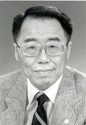
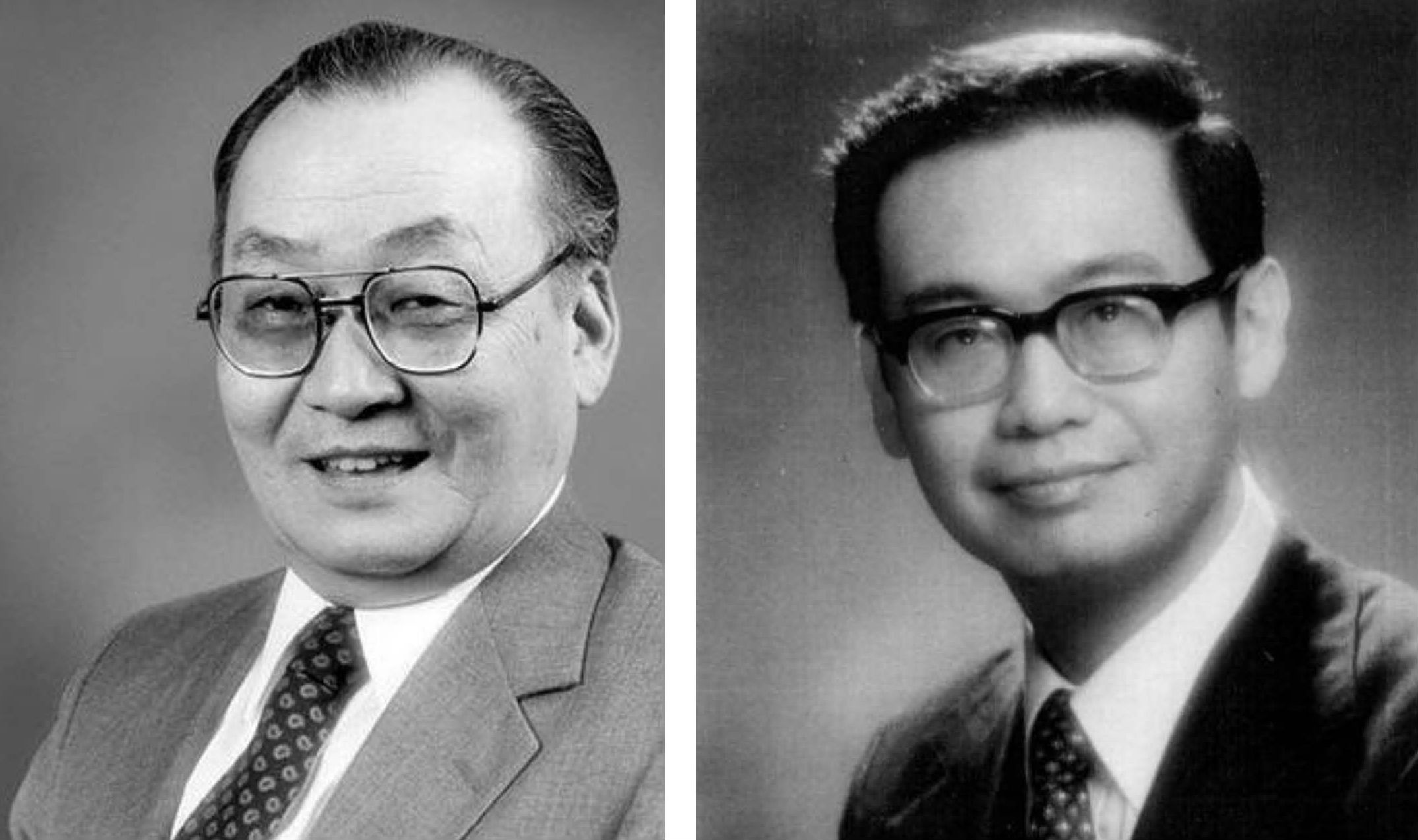
Fujio Masuoka
Arriving in Washington to defend a company in a patent litigation with TI, Masuoka came up with the idea of a NAND Flash architecture that could provide even smaller cell size and faster write / erase speeds than NOR Flash. Upon his return, Masuoka asked Hiseo Tajiri, Toshiba's head of consumer electronics development, if a digital camera with four megabit NAND flash could replace film. [ Interview with Fujio Masuoka ] Tajiri realized that NAND could indeed replace film, and that led to the camera department funding the project. Masuoka talked about the device on the 1987 IEDM in Washington DC, and production of 16Mbit NAND Flash chips began in 1992.
Unhappy that Toshiba, in his opinion, did not sufficiently reward his work, Masuoka quit his job in 1994, becoming a professor at Tohoku University. Contrary to the company's Japanese culture of loyalty, he sued his former employer for compensation, and settled the dispute in 2006 for a lump sum of ¥ 87 million ($ 758,000).
Stefan Lai joined Intel's Santa Clara department to develop scalable EEPROM technology. Working with Dick Pashley, he devised a way to add electrical erase functionality to pre-existing small EPROM cells to create a NOR Flash architecture that could be fabricated using a standard manufacturing process. NVM said the technology would not work, so Lai and Pashley met with Gordon Moore, who told them, "I'll get it done, don't fuss." [ Interview with Intel Flash ] After starting the development of a new Flash-based business device in Folsom, California, Pashley and Lai, along with designer Niles Kynett, demonstrated working chips in 1986, and released the 256-kilobit NOR Flash product in 1987. ...
By the late 1980s, the global market for semiconductor NVM devices of all manufacturing technologies exceeded $ 2 billion. The most popular products of that era were 64Kbps, 128Kbps, 256Kbps and 1Mbps EPROMs, and the first 2Mbps devices began to appear. US manufacturers, led by AMD, Intel, Motorola, SEEQ and TI, received approximately 50% of global market profits. The remaining profit was split between European, mainly SGS-Thompson (10%), and Japanese suppliers Fujitsu, Hitachi, Mitsubishi, NEC, Oki, Toshiba (40%), but their supplies were limited by government production quotas (MITI).
1990s - Solid State Drives and New Consumer Applications
In the 1990s, Flash technology created new possibilities for NVM devices in both NAND and NOR configurations. The NOR Flash architecture had the advantages of random access and fast read times, and its execute-in-place (XIP) functionality was ideal for code execution and thus for data processing. NAND Flash had slower read speeds, but a much smaller cell size, allowing for low-cost, high-density devices, ideal for external storage. In addition, read / write access to NAND blocks simulated access to disk drives.
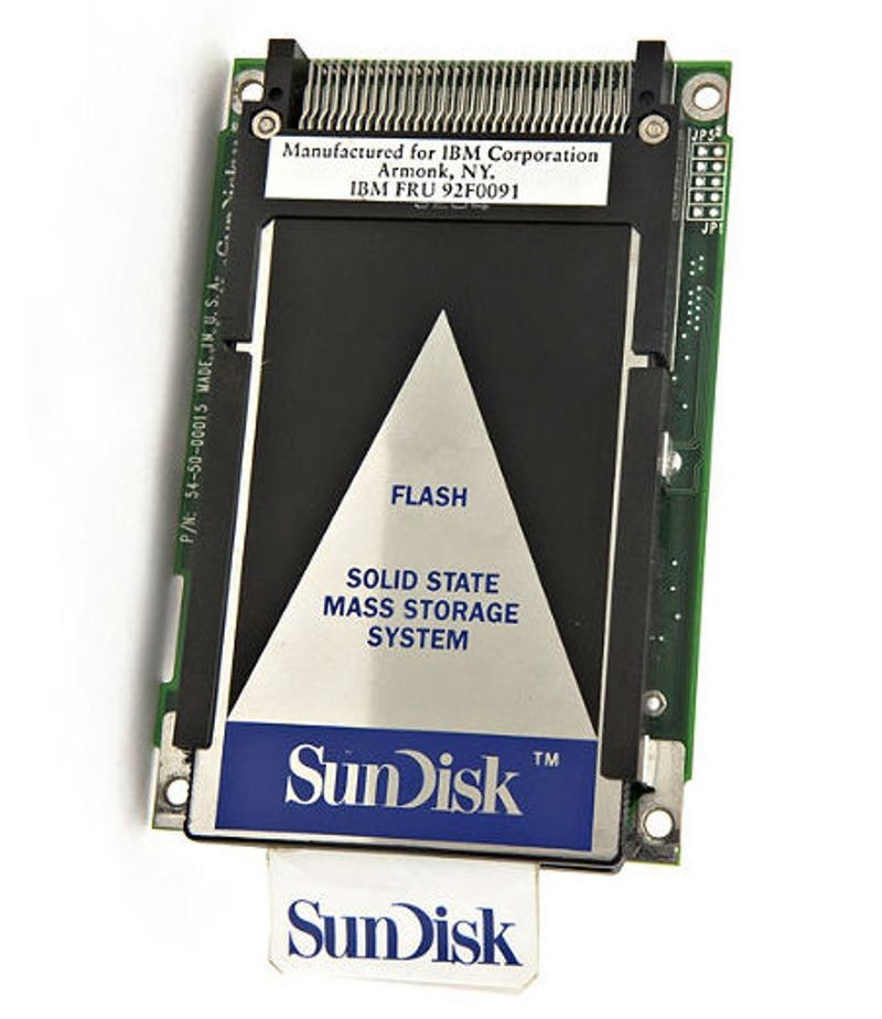
SanDisk (formerly SunDisk) SSD prototype for IBM (1991)
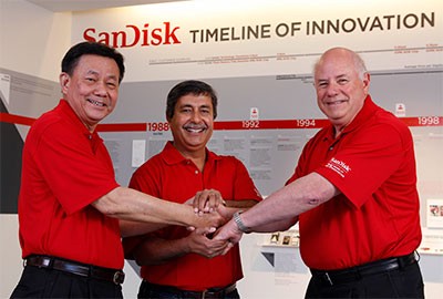
Eli Harari, who pioneered thin oxide processes at Hughes Aircraft in the 1970s, founded SunDisk (later renamed SanDisk) in 1988 to develop flash memory-based high-capacity memory devices. He was soon joined by co-founders Jack Yuan and Sanjay Mehrotra, and systems architect Robert "Bob" Norman. The company's first major order was 10,000 plug-and-play 20MB 2.5-inch ATA devices to replace the 20-megabyte Connor hard drive in IBM's ThinkPad PC in 1991. At the time, flash memory reliability was low, but Harari was encouraged by customer feedback on prototype devices: "If multiple devices run smoothly for me all weekend, you have a good product." [ Interview with Eli Harari]
Several generations of improvements to the manufacturing process and architecture of flash memory systems have been required to achieve the levels of reliability required for commercial applications. Harari embedded metadata into the devices that allowed his firmware to perform error correction, thus hiding from the user the reliability issues - critical to the technology's popularity. Mainstream laptops with SSDs hit the market in the late 2000s, and modern SSDs are the fastest growing segment of the computer storage market.
SanDisk Founders: Yuan, Mehrotra, and Harari
SanDisk's new opportunity came after the company introduced CompactFlash cards for digital cameras in 1994. “We realized that instead of someone else selling film or camera sellers, we needed to create a secondary market for flash cards. Its transformation into an international brand was a turning point in the company's history, ”says Mehrotra. [ Interview with Sanjay Mehrotra ] In 2016, SanDisk was acquired by Western Digital.
Today's flash technology dominates the $ 50 billion NVM market in 2019 and is the largest segment in the global semiconductor industry. Samsung has become the largest supplier of flash chips with approximately 30% of the market. Other major suppliers are Toshiba and Western Digital.
Flash Memory Summit Achievement Award
Each year, the Flash Memory Summit honors individuals who have shown leadership in advancing the development, use of flash memory and related technologies with the Lifetime Achievement Award (LAA) . Nominees not mentioned above included Samsung's Kinam Kim, who received an award for his progress in 3D NAND development, and Dov Moran and Aryeh Mergi of M-Systems for innovations, including embedded flash memory in mobile phones, file systems for Flash and USB flash drive.
Links
1. C. T. Sah, “A new semiconductor tetrode, the surface-potential controlled transistor,” Proceedings of the IRE, vol. 49, no.11, (Nov. 1961) pp 1625.
2. C. T. Sah, “Evolution of the MOS transistor — from conception to VLSI,” Proceedings of the IEEE, Vol. 76, №10 (October 1988) p. 1295.
3. Edgar A. Sack and David A. Laws, “Westinghouse: Microcircuit Pioneer from Molecular Electronics to ICs,” IEEE Annals of the History of Computing, Vol. 34 (Jan.-March 2012) pp. 74–82.
4. Wegener, H.A.R., Lincoln, A.J., Pao, H.C., O’Connell, M.R., Oleksiak, R.E. Lawrence, H. “The variable threshold transistor, a new electrically-alterable, non-destructive read-only storage device,” Electron Devices Meeting, 1967 International, Vol. 13 (1967) p. 70
5. H. A. R. Wegener, “Investigation of New Concepts of Adaptive Devices,” NASA-CR-86114, Report no. SRRC-CR-68–43, Sept. 1968.
6. Dov Frohman-Bentchkowsky, “Integrated MNOS memory organization” US Patent 3641512A
7. Neale, R. G., D. L. Nelson, Gordon E. Moore, “Nonvolatile and reprogrammable the read-mostly memory is here,” Electronics (September 28, 1970) pp. 56–60.
8. Tarui, Yasuo; Hayashi, Yutaka; Nagai, Kiyoko “Proposal of electrically reprogrammable non-volatile semiconductor memory”. Proceedings of the 3rd Conference on Solid State Devices, Tokyo. The Japan Society of Applied Physics (1971–09–01): 155–162.
9. “MOS EPROM Forecast,” Dataquest SIS Prod., Mkt., & Tech. Report 0004718 (August 1989) p. 2
Links to interview transcripts
, №0341, Science History Institute
, 102702214, Computer History Museum Collection
, 102745933, Computer History Museum Collection
Flash Intel, 102658199 Computer History Museum Collection
, 102740455, Computer History Museum Collection
, 102746703 Computer History Museum Collection
, 102746703 Computer History Museum Collection
, 500001027 Computer History Museum Collection
Interview with Charles C., catalog 102746598 Computer History Museum Collection
Interview with Simon Zee, catalog 102746858 Computer History Museum Collection
Advertising
Our epic servers use only triple replicated NVMe NAS . You can use the server for any task - development, hosting sites, using a VPN, and even getting a remote machine on Windows! There can be a lot of ideas and we will help to translate any of them into reality!