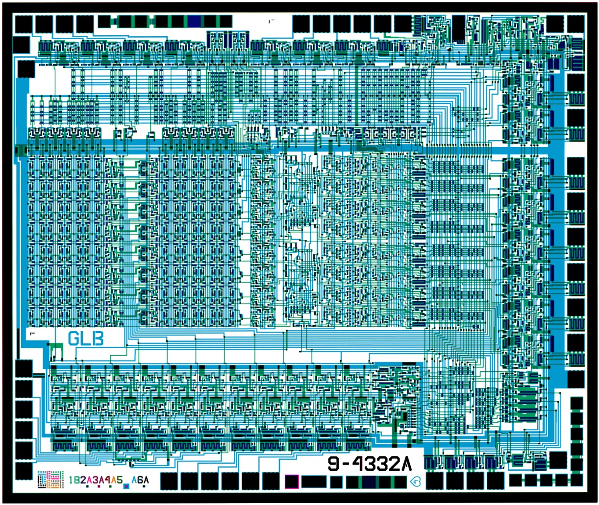
Nanoprocessor combined photomasks. GLB to the left of the data bus is the initials of developers George Latham and Larry Bauer.
The HP Nanoprocessor is an almost forgotten processor developed by Hewlett-Packard in 1974 (for more details, see The Forgotten Ones: HP Nanoprocessor , HP9825.com and The HP 9845 Project ) as a microcontroller for various company products. It is strange that this processor could not even add or subtract - perhaps that is why they decided to call it not a processor, but a “nanoprocessor”. Despite these limitations, Nanoprocessor controlled a variety of devices from Hewlett-Packard, from front-end panels and voltmeters to spectrum analyzers and data acquisition terminals.
I have determined that Nanoprocessor has been specifically used in the following products from Hewlett-Packard: HP 9845B Spectrum Analyzers, HP 3585A , HP 3325A Synthesizer / Function Generator , HP 9885 Floppy Drive , HP 3070B Data Acquisition Terminal , HP 98034 HPIB interface for HP 9825 calculator, real-time clock HP 98035 for the HP 9825 computer, the interface of film drive HP 7970E , router HP 4262A , the spectrum analyzer HP 3852 , voltmeter HP 3455A... Paul-Henning Camp also told me that Nanoprocessor was used in the HP 3336 synthesizer / function generator and the HP 9411 switch controller. The
key feature of the Nanoprocessor was its low cost and high speed: compared to its current Motorola 6800, the Nanoprocessor cost $ 15, not $ 360 , and coped with management tasks an order of magnitude faster.
It is interesting that the competitor of Nanoprocessor in its development was the Motorola 6800, and not the processor from Intel. The main thing that the Nanoprocessor could boast of was speed: it worked at 4 MHz, considering that the 6800 worked at 1 MHz. Both processors took 2 clock cycles to execute a basic instruction, while the 6800 took up to 7 clock cycles to execute more complex instructions.
The Nanoprocessor developers put together a speed comparison and suggested that Nanoprocessor could read six times faster than the 6800 and handle interrupts more than 16 times faster. However, it was then assumed that the Nanoprocessor would operate at 5 MHz, and the real chip fell slightly short of this bar with its 4 MHz. The preliminary price of Nanoprocessor was called $ 15 versus $ 360 for the Motorola 6800.
I do not quite agree that Nanoprocessor can be called a microcontroller, since it uses an external ROM with a program, whereas a microcontroller usually has everything, including the ROM, on one chip (in this aspect it looks like Intel 4004). However, in almost all respects Nanoprocessor resembles a microcontroller: it is designed for embedded use, its Harvard architectureand the instruction set is optimized for I / O, it runs programs from ROM with minimal data storage.
As for computers that could not add - the IBM 1620 computer the size of a table from 1959 did not have an addition operation, but used a table of results for this. His codename was CADET, and people jokingly deciphered it as "Can't Add, Doesn't Even Try" [can't add and doesn't even try].
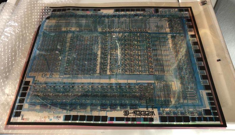
Recently, chip designer Larry Bauer published six photomasks used to produce Nanoprocessor, along with details of their design. The photomasks were cleaned and scanned in The CPU Shack, and then cleaned by Antoine Berkovichi (122 MB PSD file can be downloaded from the link). The composite image of the photomasks below shows the internal circuits of the IC. The blue layer is the top metal layer of the chip, the green one is the bottom silicon layer. Black squares around the perimeter - 40 pads for communication with external contacts of the IC. I used these photomasks to reverse engineer the processor to understand its simple yet clever RISC-like circuitry.
Nanoprocessor is very similar to the Reduced Instruction Set Computer (RISC) processor, although it appeared several years before such a concept. In particular, Nanoprocessor is designed with a simple instruction system, all instructions are executed in one clock cycle (after the sampling clock), the register set is large and orthogonal, and the addressing is simple. These inherent characteristics of RISC have resulted in higher clock speeds compared to more complex processors.
Nanoprocessor was developed in 1974, at the same time that the classic Intel 8080 and Motorola 6800 processors were announced. However, the Nanoprocessor silicon manufacturing process lagged by several years - they used metal-gate transistors instead of silicondeveloped in the late 1960s. The difference seems confusing, but silicon gates were better on several counts . First, they are smaller, faster and more reliable. Second, they had a polysilicon layer with conductors other than metal; as a result, the chip layout was almost twice as dense. Third, metal-gate transistors required an additional + 12V power supply. The Intel 4004 processor used silicon gates in 1971, so I'm surprised HP still used metal in 1974.
Given these limitations, I am impressed with the Nanoprocessor's wiring density - one layer of metal, no polysilicon. I looked for other metal gate chips and their wiring is terribly inefficient - there are more conductors than transistors. At the same time, the Nanoprocessor chains are located efficiently and do not waste extra space.
Nanoprocessor technology outperformed Intel 8080 and Motorola 6800 in one thing: it used depletion-mode pull-up transistors, which were more advanced than enhancement-mode transistors used in 8080 and 6800 The first technology provides logic gates that are faster and consume less, but require an additional production step. At Nanoprocessor, Photomask # 3 (gray) was used in this step. Processors such as the MOS Technology 6502 and the Zilog Z80, pull-up transistors with their own channel allowed them to operate at one voltage, not three. Unfortunately, the Nanoprocessor still required different voltages due to the metal gate transistor.
A very strange characteristic of Nanoprocessor is the alternating bias voltage of the substrate. For speed reasons, many 1970s microprocessors applied negative voltage to the silicon substrate, with -5 V applied through the bias contact. Nanoprocessor has a bias pin, but it is strange that the bias voltage varies from chip to chip, from -2 V to -5 V. During production, the required voltage was written on the chip by hand (see below). Each Nanoprocessor had to be installed with a matching resistor to get the correct voltage. If the Nanoprocessor was changed on the board, the resistor had to be changed as well. Variable bias looks like a manufacturing flaw - I can't imagine Intel doing this in processors.
Early DRAM chips and microprocessors often required three supply voltages: +5 V (Vcc), +12 V (Vdd), and -5 V (Vbb) offset voltage. In the late 1970s, improvements in manufacturing technology made it possible to use a single voltage. The 1974 Intel 8080 microcontroller used induced channel transistors that required three voltages, but an improved version of the 8085 (1976) used a transistor with its own channel and was powered by a single + 5V voltage. Since the late 1970s, many microprocessors have used charge pump generators. located on the chip to generate a negative bias voltage.

HP Nanoprocessor part number 1820-1691. Note the handwritten voltage: -2.5 V. The last digit of the part number (1) is also handwritten and represents the speed of the chip.
Like most processors of that era, Nanoprocessor was 8-bit. It didn't use random access memory, however, but ran the code from a 2KB external ROM. It had 16 8-bit registers - more than most processors and enough to compensate for the lack of memory in many applications. In terms of the number of transistors, Nanoprocessor is more complex than Intel 8008 (1972) and slightly easier than 6800 (1974) or 6502 (1975).
According to my calculations, the Nanoprocessor has 4639 transistors. The instruction decoder is made up of pairs of small transistors based on location considerations. The combination of these pairs results in 3829 unique transistors. Of these, 1061 are pull-ups and 2668 are active. For comparison, the 6502 had 4237 transistors, of which 3218 were active. The 8008 had 3500 transistors, while the Motorola 6800 had 4100.
But its architecture uses transistors for a different purpose than these processors. Nanoprocessor lacks an ALU, but instead has a large set of registers taking up most of the die area. Nanoprocessor has 48 teams, significantly less than the 6800 with 72 teams. However, Nanoprocessor has handy set, reset, and bit check operations that the mentioned processors did not have. Nanoprocessor supports access to registers by index, but it does not have complex addressing modes like other processors.
Early microprocessors did not have bit set, reset and check operations (although they can be implemented via AND and OR). The Z80 (1976) added bitwise operations, but they were two bytes each and were much slower than Nanoprocessor.
The block diagram below shows the internal structure of Nanoprocessor. The main I / O feature is the 4-bit "I / O Instruction Device Select", which allows 15 devices to receive I / O commands. In other words, the selected pins determine which I / O device is reading or writing from the data buses. External circuits use these signals for everything a particular application needs - storing data in a latch, sending to another system, reading values. Even more I / O is provided through Direct Control I / O pins (GPIO pins), suitable for input and output. If these pins are not connected to external circuits, they act as convenience bit flags; Nanoprocessor can set a value and then read it.In the absence of an arithmetic logic module, the control logic module performs increment, decrement, shift operations and bit operations on the adder.

Block diagram from the Nanoprocessor user manual
I reverse-engineered the Nanoprocessor based on photomasks and mapped the placement of the functional blocks on the die. The largest element is a set of 16 registers to the left of center. On the right is the comparator and adder, together with their increment, decrement, shift and complement circuits. The instruction decoder takes up most of the space above and to the right of the battery comparator. The bottom of the chip is mainly occupied by an 11-bit instruction counter, as well as a single-entry interrupt stack and a subroutine stack. The control circuits implement the simplest command synchronization: one extraction cycle is followed by one execution cycle. Most microprocessors have control circuits that take up a significant portion of the chip, but Nanoprocessor control circuits are small blocks.
Nanoprocessor adheres to its model of executing instructions in one cycle, even for double-byte instructions: the second byte is requested during the cycle of execution, so the total command execution time does not change.
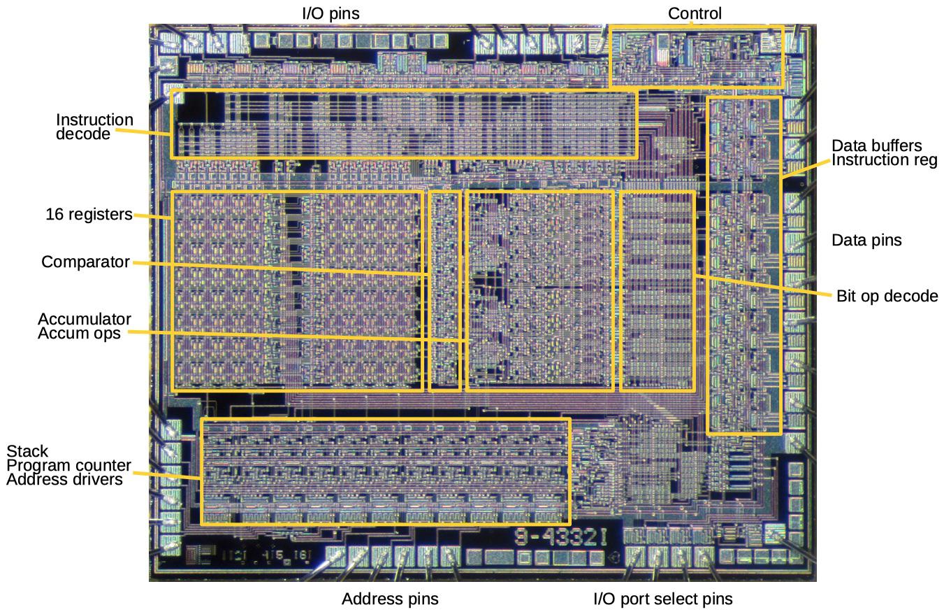
HP Nanoprocessor functional components
Understanding photomasks
The chip was fabricated using six photomasks, each of which was used to produce one of the processor layers by means of photolithography . The photo below shows photomasks. Each is a 47.2 x 39.8 cm Mylar sheet . These are 100x magnified photomasks used to produce a 4.72 x 3.98 mm silicon crystal (33% smaller than the 6800 crystal). Each 3-inch silicon wafer contained about 200 ICs, which were produced at the same time, then tested, cut and placed in a package.
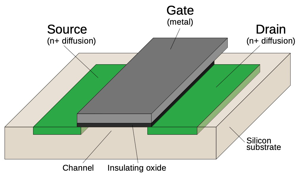
To explain the role of masks, I'll start by describing the metal gate MOS structure used in the Nanoprocessor. In the diagram below, two sections of silicon (green) are made conductive with the help of impurities, and form the source and drain of the transistor. A metal strip between them forms a gate, separated from silicon by a thin layer of insulating oxide (hence the name of the structure - Metal, Oxide, Semiconductor). The transistor can be thought of as a switch controlled by the gate. Also, the metal layer provides the main method for connecting IC components with conductors, although some conductors also extend over the silicon layer.
Schematic of a MOS structure with a metal gate
Photomasks are a key part of the IC manufacturing process as they locate components. The diagram below shows how impurities are added to some areas of silicon using photomasks. First, an insulating oxide layer is formed on the silicon substrate, then a photosensitive photoresist is added... Ultraviolet light (1) polymerizes and cures the photoresist everywhere except where the mask blocks the passage of light (2). Then the soft photoresist that has not been exposed to ultraviolet radiation is removed (3). The substrate is exposed to hydrofluoric acid, which removes the oxide layer where it is not protected by the photoresist (4). Holes appear in the oxide that correspond to the pattern on the photomask. Then the substrate is exposed to a hot gas that penetrates into unprotected areas of silicon and changes its conductive properties (5). This process generates small areas of silicon with impurities, corresponding to the picture on the photomask (6). Other photomasks are used for other production steps, but they use the same process using a photoresist.
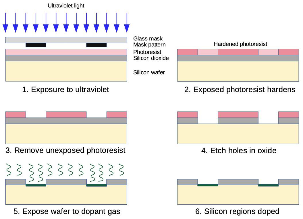
How impurities are added to the silicon regions using photomasks I will
enlarge one section of the Nanoprocessor to show how one circuit is formed from six photomasks (which is an inverter that changes the binary value supplied to the input). Using the first photomask and the above-described photolithography process, the silicon portions are made conductive. The green marked areas with impurities will form the sources / drains of the transistor or the junction of components.
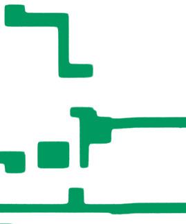
The first photomask creates patches of conductive silicon
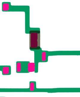
The crystal is then covered with an insulating oxide layer. The second photomask (purple) is used to etch holes in the oxide that expose the underlying silicon. These holes can be used to create the gates of the transistor as well as the connection of metal conductors and silicon.

The second photomask creates holes in the oxide layer.
The third photomask (gray) exposes areas for the implantation of ions that change the properties of silicon and, therefore, the transistor. This turns the upper transistor into a channelized transistor that pulls the output of the logic gate up.
The third photomask (gray) creates impurities in the silicon of the upper transistor
The silicon is then coated with an additional thin layer of insulating oxide to form the gate oxides for the transistor. The fourth photomask (orange) removes this oxide from those areas that will become contacts between silicon and the metal layer. After this step, most of the crystal is covered with a thick insulating oxide. Above the gates of the transistor (purple), the oxide layer is very thin, and it has holes for contacts from the current photomask (orange).
The fourth photomask creates holes in the oxide
The fifth photomask (blue) is used to create metal conductors from above - for this, a uniform layer of metal is first applied, and the unnecessary parts are then etched away. In those places where the fourth mask created holes in the oxide, the metal layer comes into contact with silicon and forms a conductive contact. Where the third mask has created a thin layer of oxide, the metal layer forms the gate of the transistor between the two pieces of silicon. Finally, the entire substrate is covered with a protective vitreous layer. The sixth photomask is used to create holes in this layer above the contacts at the edges of the chip. After cutting the entire substrate into individual crystals, a wire welding is soldered to these contacts, connecting them to the external contacts.
The fifth photomask creates a metallic layout
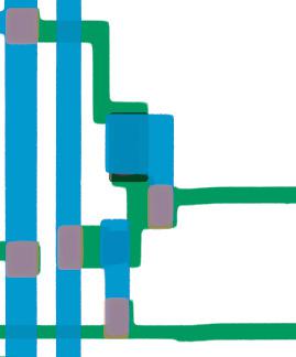
The diagram below shows how this circuit forms an inverter with two transistors. The two symbols of the transistor correspond to the two transistors obtained using the photomask. In the absence of an input signal, the upper transistor (connected to +5 V) pulls the output up. When the input signal is high, it turns on the lower transistor. This connects the outlet to ground, pulling the outlet down. Thus, the circuit inverts the input signal.
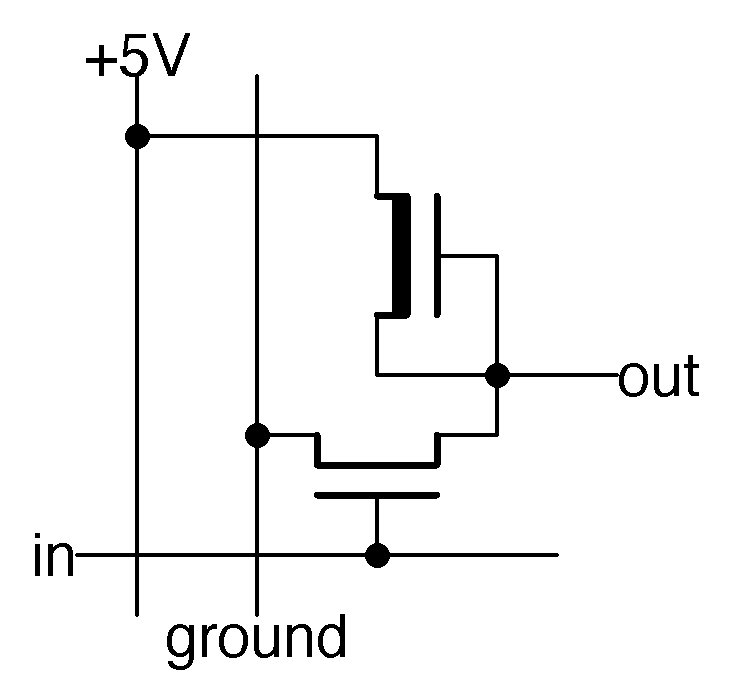
N-MOS inverter circuit matching the templates above
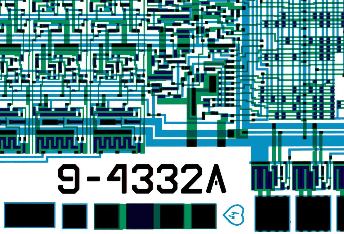
Although the diagrams above show a single inverter, these steps using photomasks to create a complete processor with all 4,639 transistors. The diagram below shows a larger portion of the die, where dozens of transistors form more complex gates and circuits. I noticed one touching thing on one of the photomasks - a tiny heart with the letters HP inside, under the chip number.
Nanoprocessor has two different part numbers. 1820-1691 denotes a 2.66 MHz version and 1820-1692 denotes a 4 MHz version. The last digit was written manually on each chip after being verified in the case. The part number is not related to the 9-4332A chip number on the die.
Chip drawings
How Nanoprocessor controls the clock
To understand how Nanoprocessor was used in practice, I reverse engineered the code from the HP 98035 clock module. The module connected to an HP 9825 desktop computer and served as a real time clock, and could also measure intervals and trigger periodic events with millisecond precision. The clock module circuit was rather unusual. To keep the current time when the computer is off, the clock module was built on the basis of a digital clock chip with a spare battery. The clock chip was not designed for computer control, which caused inconvenience: it generated 7-segment signals to control LEDs, and was configured with three buttons. To find out the time, Nanoprocessor had to convert the output from the 7-segment display back to numbers.To set the Nanoprocessor time, you had to emulate the correct sequence of button presses.
The HP 9825 was a 16-bit desktop computer with support for a language similar to BASIC. Introduced in 1976, five years before the IBM PC, it was a pretty advanced system for its time. At the back, it had three connectors for adding modules such as a real-time clock module.
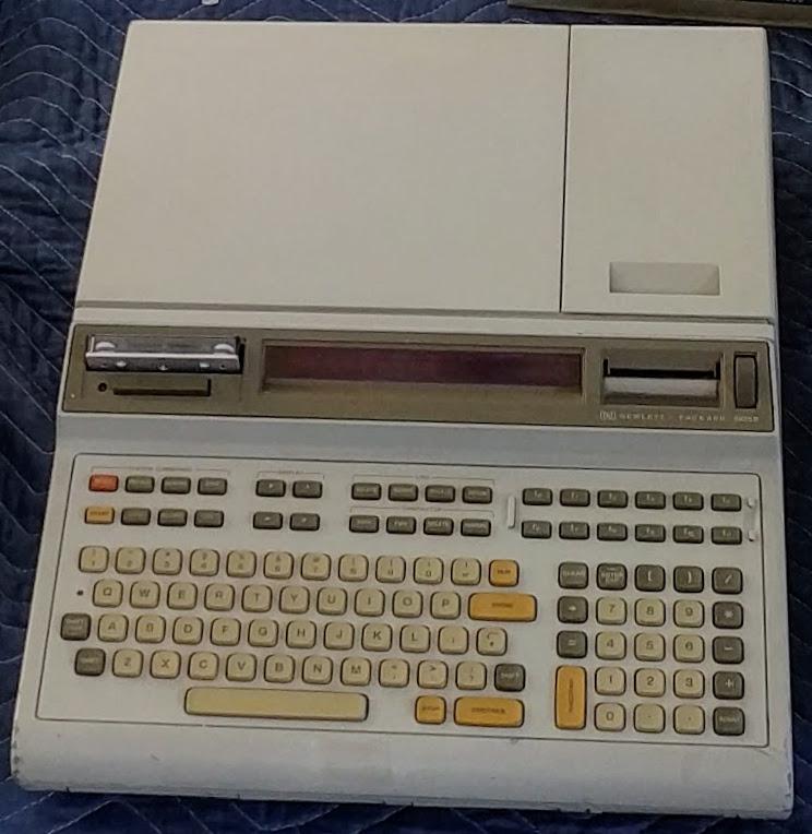
HP 9825 with LED display, tape drive and printer
To save energy, the clock chip from Texas Instruments is implemented on integrated injection logic (I2L). Low power chips would use CMOS today, but that was rare back then. I2L was built on bipolar transistors, similar to TTL, but using different circuits with high density and low power consumption. Perhaps it was an X-902 chip in a DIP package.
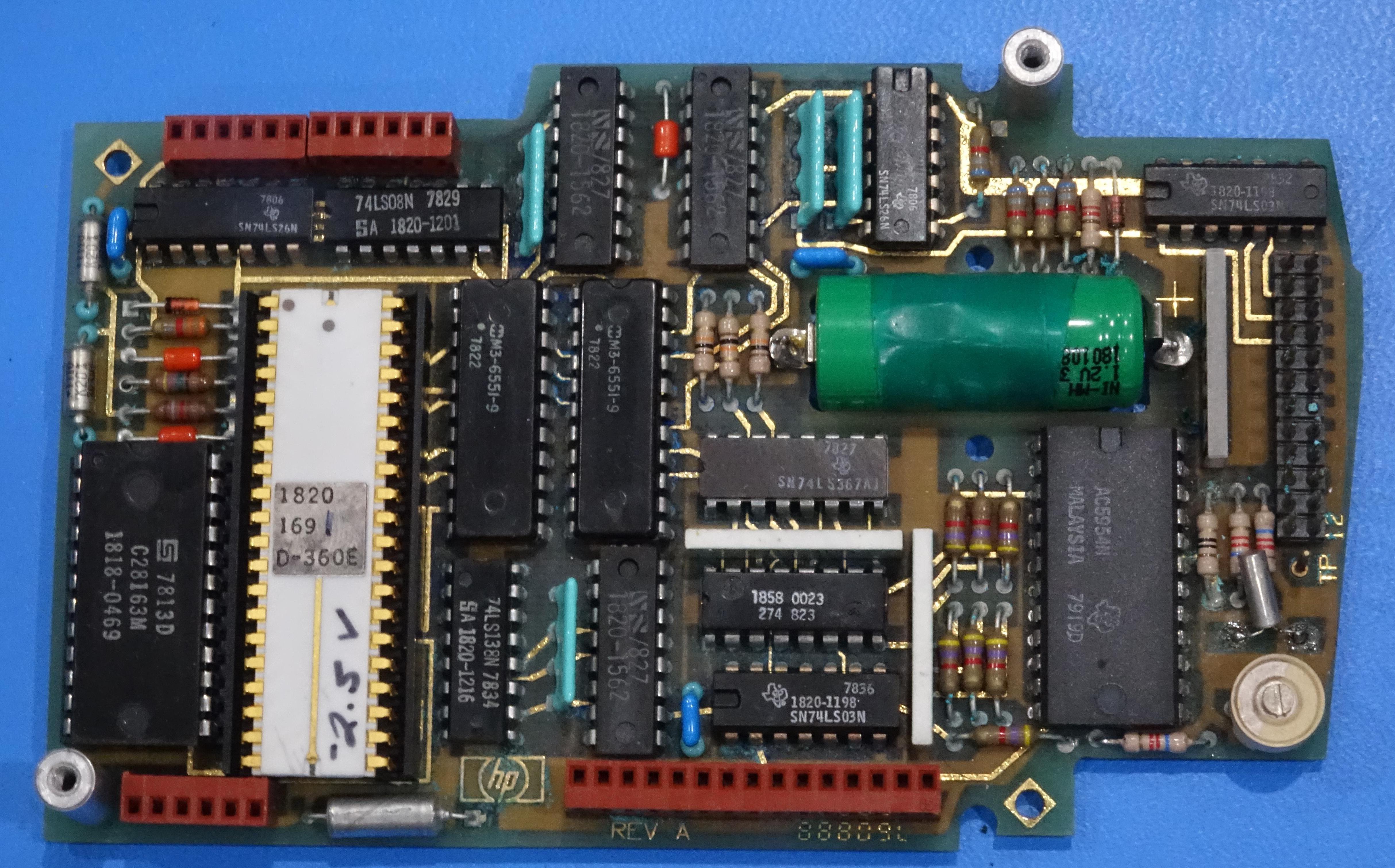
Nanoprocessor (white chip) as part of the HP clock module. To the left of it is a 2KB ROM. On the right are two 256-bit x 4 memory chips. The Texas Instruments clock chip is a large black chip underneath the green NiCad battery The
computer controlled the clock module by sending it ASCII strings of characters like "S 12: 07: 12: 45: 00", which should have set the time to 12:45:00 December 7 (or July 12 in European notation). The various interval timers, alarms and counters of the module were initiated in a similar way, through commands such as "Unit 2 Period 12345". The module supported 24 commands, and Nanoprocessor needed to recognize them .
Here is a piece of code reverse engineered from the clock board ROM. This is the code from the interrupt handler that increments the timer and date every second. The code determines the number of days in a month so that it knows when to change the month to the next. Columns - byte values, commands and my explanations. This code gets the month number (01-12 BCD), stores it in the accumulator, and returns the number of days of the month (28, 30 or 31 BCD) in register 0. Not bad for 16 bytes of code, despite ignoring leap years. How does he work? For months after 7 (July) it subtracts 1. Then, if the month is odd, then it has 31 days, and if it is even - 30. To process February, the code clears the 1 month bit. If the month becomes 0 (February), then it has 28 days.
d0 STR-0    (7)   0.


07


0c SLE    ,   <=  0.


03 DED    1


5f NOP


d0 STR-0    (0x31)   0


31


30 SBZ-0    ,   0   0


81 JMP-1   0x1c9 (  )


c9


a1 CBN-1   1


d0 STR-0    (0x30)   0


30


0f SAN    ,      0


d0 STR-0    (0x28)   0


28
You can see from the code that even if a processor without an addition operation seems useless, the bitwise operations and the Nanoprocessor increment / decrement allow more calculations than you might think.
In the code, I came across a place where I need to add two BCD numbers and form one byte. This was done by a cycle that decreased one number and increased another. When the first number reached zero, the second got their sum. So, even without ALU, the addition can be carried out, albeit slowly.
You can also see that the Nanoprocessor code is compact and efficient. You can do a lot in one byte, which in other processors takes several bytes. A large set of Nanoprocessor registers allows you to avoid dreary data swapping to and fro. While some consider Nanoprocessor to be more of a state machine than a microprocessor, this would be an understatement of the capabilities and role of Nanoprocessor.
Although the Nanoprocessor does not have ALUs or random access memory commands, they can be connected as additional I / O devices. The watch has a 256-byte random access memory that stores the values of counters and timers, access to which is organized through the I / O ports. Other products added ALUs to support arithmetic operations.
The clock board diagram shows how two 256x4 RAM chips are connected to the Nanoprocessor. The Nanoprocessor I / O port selects a pin and connects to the “3-8 Decoder” U5, which outputs separate signals for each of the I / O ports. Three of them go to the control pins of the RAM chip, and one controls the chips of the data latches U9 and U10, which hold the written data.

All I / O ports use the Nanoprocessor data bus (top) to exchange data, so the bus connects to both the address pins of the RAM chips and the data pins. For reading, the memory address is written to the chips through one I / O port, and then the data is read from memory through another port. In both cases, the values pass through the data bus, and the signal from "3-8 Decoder" indicates what to do with the values. For writing, the first I / O operation stores the byte value in the latches, and then the second I / O operation sends the address to the memory chips. This might sound like a clumsy Goldberg machine -style approach , but in practice it works well and read / write can be done with two bytes of instructions.
Many processors, such as the 6502, use memory mapped I / O — devices are mapped to the memory address space and accessed through read / write operations. Nanoprocessor works the other way around, plugging memory into an I / O port and accessing it through I / O operations.
When adding ALUs, a similar approach is used- as in the HP 3455A voltmeter using two Nanoprocessors. The voltmeter uses two 74LS181 ALU chips to implement an 8-bit ALU, which it uses to scale the values and calculate the percentage of error. Two exit ports provide arguments, and one defines an operation. The 8-bit result is read from the port, and the processor reads the transfer through the GPIO pin (makes you wonder if it was easier to use a processor with arithmetic support).
Outcome
Nanoprocessor is an unusual processor. At first glance, it even seemed to me a "fake processor", due to the lack of basic arithmetic operations. The chip is based on outdated metal gate technology that lagged behind other microprocessors for several years. The strangest thing is that each chip required its own voltage, which was manually written on the case, which indicates the difficulties with stable quality in production. However, Nanoprocessor in the role of a microcontroller worked quickly, much faster than other modern processors. Hewlett-Packard used Nanoprocessor in many products in the 1970s and 1980s, in more sophisticated roles than might be expected.
Although Nanoprocessor is long forgotten, and not even written about on Wikipedia, the photomasks recently published by its creator shed light on this unusual corner of processor history.