Since the invention of its first GPU in 1999, NVIDIA has been at the forefront of 3D graphics and GPU-accelerated computing. Each NVIDIA architecture is carefully designed to deliver revolutionary levels of performance and efficiency.
The A100, the first GPU with NVIDIA Ampere architecture, was released in May 2020. It provides tremendous acceleration for AI training, HPC, and data analytics. The A100 is based on the GA100 chip, which is purely computational and, unlike GA102, is not yet gaming.
GA10x GPUs are based on the NVIDIA Turing GPU architecture. Turing is the first architecture in the world to offer high-performance real-time ray tracing, AI-accelerated graphics and professional graphics rendering, all in one device.
In this article, we will analyze the main changes in the architecture of the new NVIDIA video cards compared to their predecessor.

Figure 1. Architecture Ampere GA10x
Main features of GA102
GA102 is manufactured using NVIDIA proprietary 8nm technology - 8N NVIDIA Custom. The chip contains 28.3 billion transistors on a 628.4 mm2 die. As with all GeForce RTXs, the GA102 is based on a processor that contains three different types of computing resources:
- CUDA kernels for programmable shading;
- RT-, (BVH) ;
- , .
Ampere
GPC, TPC SM
Like its predecessors, the GA102 consists of Graphics Processing Clusters (GPCs), Texture Processing Clusters (TPCs), Streaming Multiprocessors (SM), Raster Operator ROPs (ROPs), and memory controllers. The complete chip has seven GPC units, 42 TPCs and 84 SMs.
The GPC is the dominant high-level block that contains all the key graphics. Each GPC has a dedicated Raster Engine and now also has two ROP sections of eight blocks each, which is an innovation in the Ampere architecture. In addition, the GPC contains six TPCs, each containing two multiprocessors and one PolyMorph Engine.
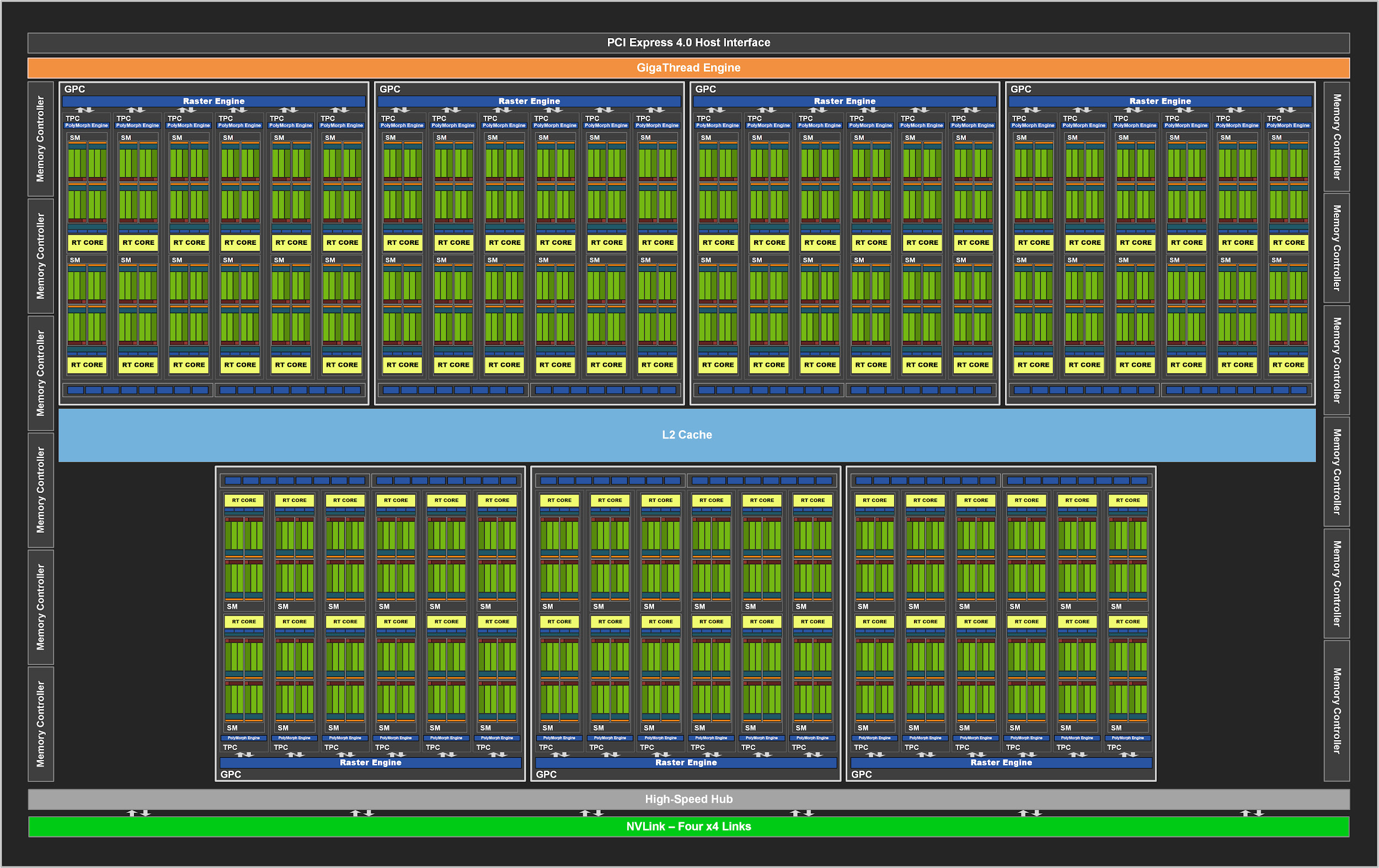
Figure 2. Complete GPU GA102 with 84 SM blocks
In turn, each SM in the GA10x contains 128 CUDA cores, four third generation tensor cores, a 256 KB register file, four texture units, one second generation ray tracing core and 128 KB L1 / shared memory, which can be configured for different capacities depending on the needs of computing or graphics tasks.
ROP Optimization
In previous NVIDIA GPUs, ROPs were tied to a memory controller and L2 cache. Starting with GA10x, they are part of the GPC, which improves raster performance by increasing the total number of ROPs.
In total, with seven GPCs and 16 ROPs in each GPC, the GA102 GPU consists of 112 ROPs instead of 96, for example, in the TU102. All of this has a positive effect on multisample anti-aliasing, pixel fill rate and blending.
NVLink third generation
The GA102 GPUs support third-generation NVIDIA NVLink, which includes four x4 lanes, each providing 14.0625 GB / s of bandwidth between two GPUs in either direction. The four channels together give 56.25 GB / s of bandwidth in each direction and a total of 112.5 GB / s between the two GPUs. So, using NVLink, you can connect two RTX 3090 GPUs.
PCIe Gen 4
The GA10x GPUs are equipped with PCI Express 4.0, which offers double the bandwidth of PCIe 3.0, transfer rates up to 16GTransfers per second, and, thanks to the x16 PCIe 4.0 slot, peak bandwidth up to 64GB / s.
GA10x Multiprocessor Architecture
The Turing multiprocessor architecture was the first at NVIDIA to have separate cores to speed up ray tracing operations. Then Volta introduced the first tensor kernels, and Turing introduced advanced second generation tensor kernels. Another innovation in Turing and Volta is the ability to simultaneously execute FP32 and INT32 operations. The multiprocessor in GA10x supports all of the above features, and also has a number of its own improvements.
Unlike the TU102, which has eight second-generation tensor cores, the GA10x multiprocessor has four third-generation tensor cores, with each GA10x tensor core twice as powerful as Turing.
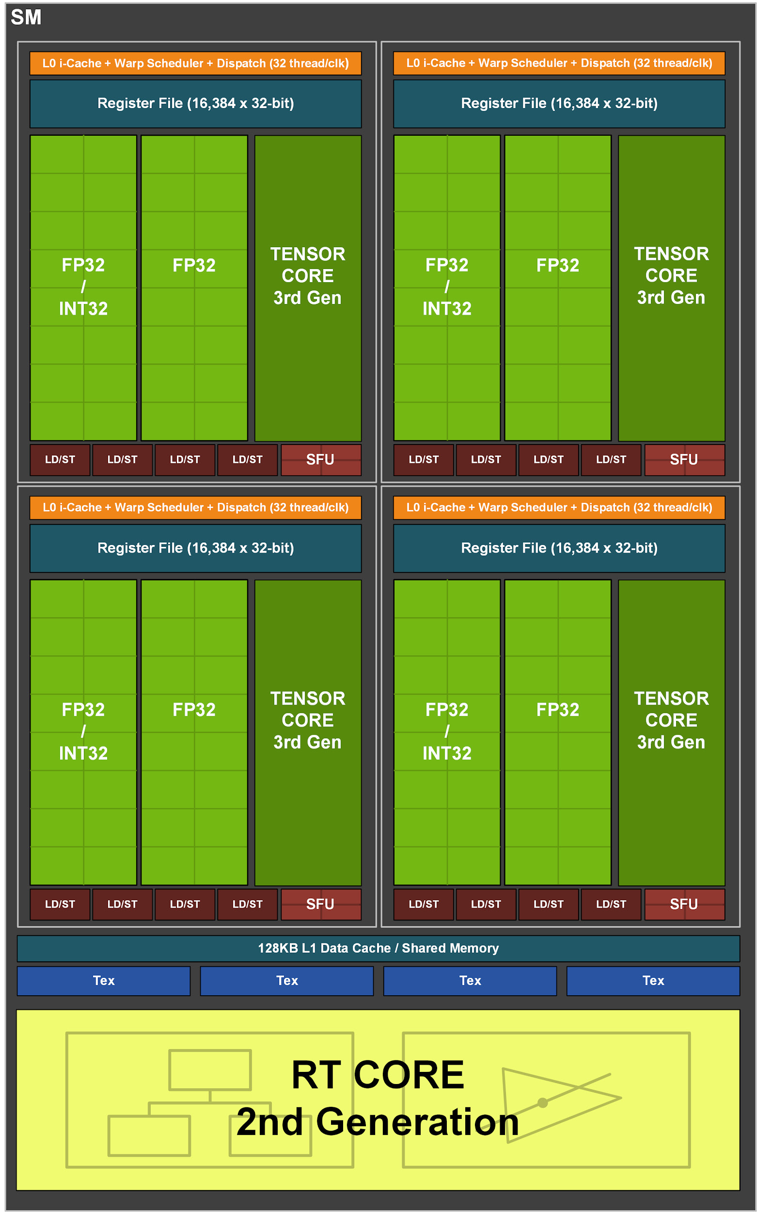
Figure 3. GA10x Streaming Multiprocessor
Double the speed of FP32 computing
Most of the graphics calculations are 32-bit floating point (FP32) operations. The Ampere GA10x Streaming Multiprocessor delivers twice the speed of FP32 operations on both data channels. As a result, in the context of FP32, the GeForce RTX 3090 provides over 35 teraflops, which is more than 2 times the capabilities of Turing.
The GA10X can execute 128 FP32 operations or 64 FP32 operations and 64 INT32 operations per clock, which is double the speed of Turing computations.
Modern gaming tasks have a wide range of processing needs. Many computations require a bunch of FP32 operations (such as FFMA, floating point addition (FADD), or floating point multiplication (FMUL)), as well as many simpler integer computations.
GA10x multiprocessors continue to support dual-speed FP16 (HFMA) operations, which were also supported in Turing. And, similar to the TU102, TU104, and TU106 GPUs, in the GA10x, standard FP16 operations are also handled by tensor cores.
Shared memory and L1 data cache
GA10x has a unified architecture for shared memory, L1 data cache, and texture cache. This unified design can be modified based on workload and needs.
The GA102 chip contains 10,752 KB of L1 cache (compared to 6912 KB in the TU102). Apart from that, the GA10x also has doubled shared memory bandwidth compared to Turing (128 bytes / cycle versus 64 bytes / cycle). The total L1 bandwidth for the GeForce RTX 3080 is 219 GB / s versus 116 GB / s for the GeForce RTX 2080 Super.
Performance per watt
All NVIDIA Ampere architectures are built to improve efficiency - from logic, memory, power and thermal management to PCB design, software and algorithms. At the same performance level, Ampere GPUs are up to 1.9x more energy efficient than comparable Turing devices.
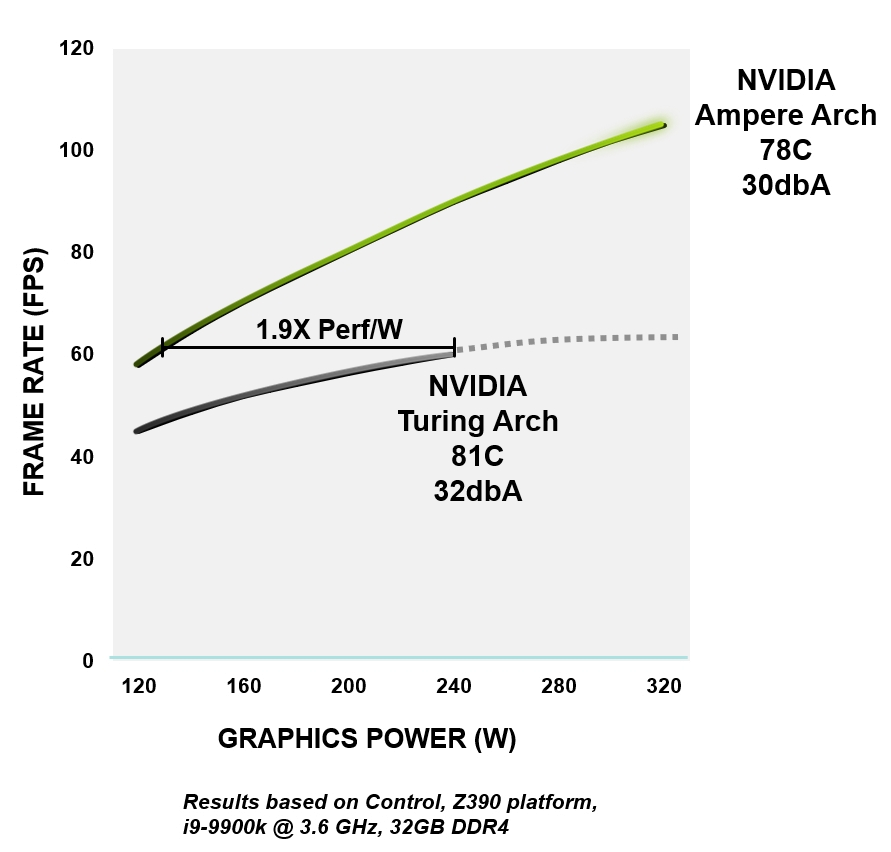
Figure 4. RTX 3080 power efficiency versus GeForce RTX 2080 Super architecture
Second generation RT cores
The new RT cores feature a number of enhancements that, combined with updated caching systems, effectively double the ray tracing performance of Ampere processors over Turing. In addition, the GA10x allows other processes to be run concurrently with RT computing, thereby significantly speeding up many tasks.
Second generation ray tracing in GA10x
GeForce RTX based on Turing architecture were the first GPUs with which cinematic ray tracing became a reality in PC games. The GA10x is equipped with second generation ray tracing technology. Like Turing, the GA10x's multiprocessors have specialized hardware blocks to check for ray intersections with BVHs and triangles. At the same time, the cores of the Ampere multiprocessors have twice the speed of testing the intersection of rays and triangles compared to Turing.
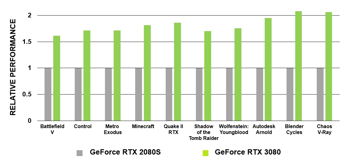
Figure 5. Comparison of performance of RT cores of GeForce RTX 3080 and GeForce RTX 2080 Super
The GA10x multiprocessor can perform operations simultaneously and is not limited to compute and graphics, as was the case in previous generations of GPUs. So, for example, in GA10x, the noise reduction algorithm can be executed simultaneously with ray tracing.
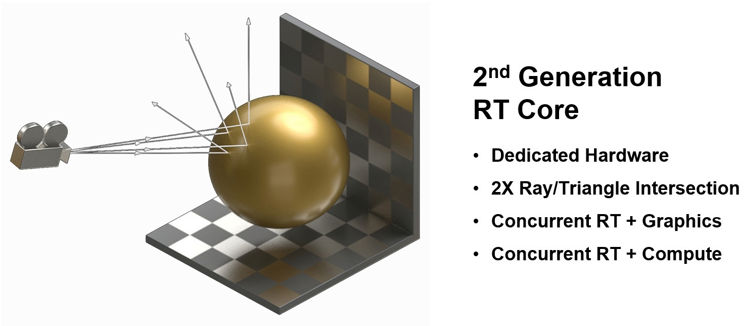
Figure 6. Second Generation RT Core in GA10x GPUs
Note that RT-intensive workloads do not significantly increase the load on the multiprocessor cores, thus allowing the multiprocessor processing power to be used for other tasks. This is a big advantage over other competing architectures that do not have dedicated RT cores and therefore have to use their building blocks for both graphics and ray tracing.
Ampere RTX processors in action
Ray tracing and shaders are computationally intensive. But it would be much more expensive to run everything with CUDA cores alone, so including tensor and RT cores helps speed up processing significantly. Figure 7 shows an example of Wolfenstein: Youngblood with ray tracing enabled in various scenarios.
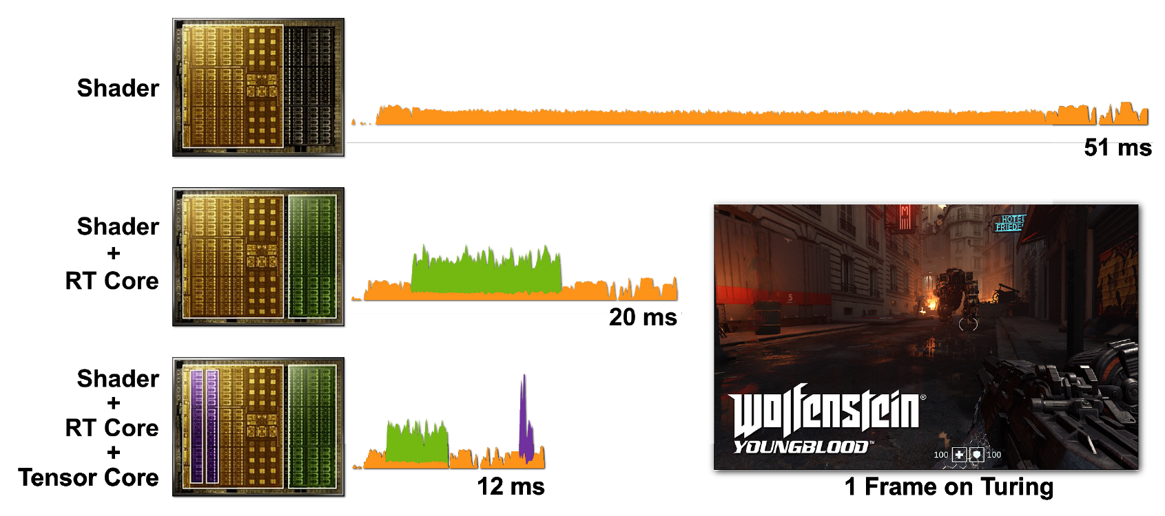
Figure 7. Rendering a single frame of Wolfenstein: Youngblood on an RTX 2080 Super GPU using a) shader cores (CUDA), b) shader cores and RT cores, c) shader cores, tensor cores and RT cores. Note the progressively decreasing frame times as you add the power of the various RTX processor cores.
In the first case, it takes 51 ms (~ 20 fps) to start one frame. When RT cores are turned on, the frame is rendered much faster - in 20 ms (50 fps). Using DLSS on tensor cores reduces the frame time to 12 ms (~ 83 fps).
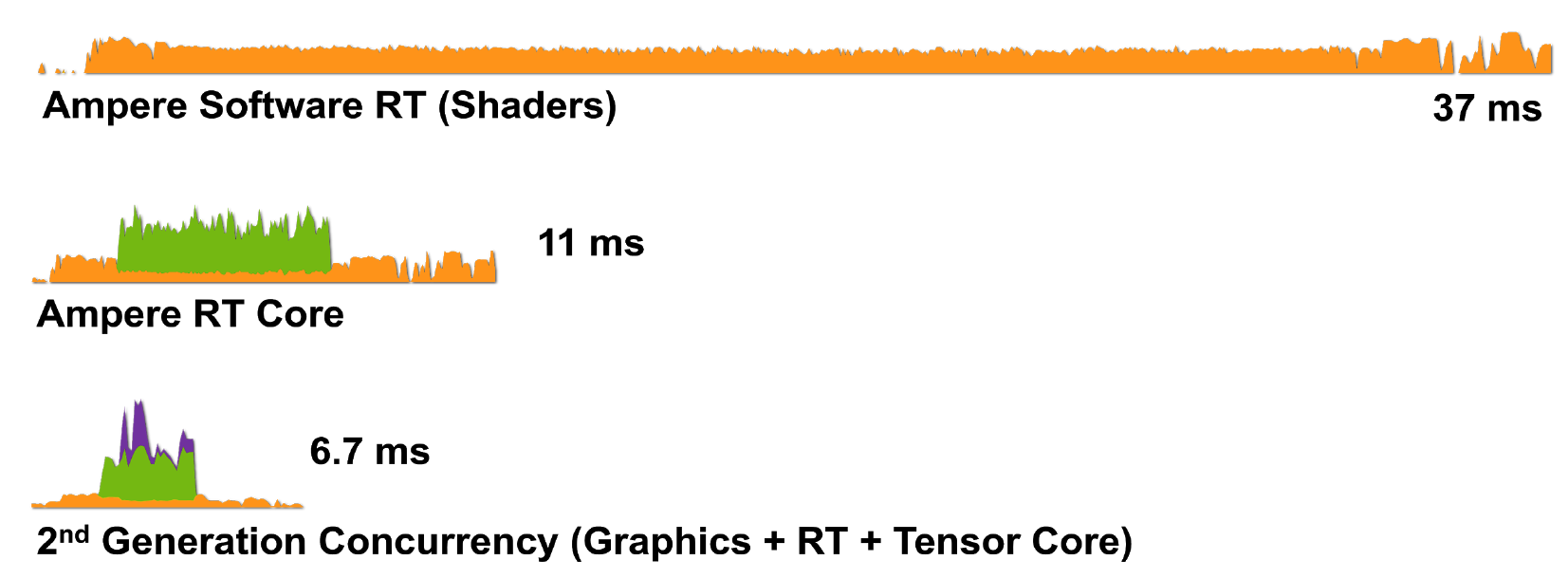
Figure 8. Rendering a single frame of Wolfenstein: Youngblood on an RTX 3080 using a) shader cores (CUDA), b) shader cores and RT cores, c) shader cores, tensor and RT cores.
So, RTX technology with Ampere architecture is even more efficient at handling rendering tasks: the RTX 3080 renders a frame in 6.7 ms (150 fps), which is a huge improvement over the RTX 2080.
Hardware accelerated ray tracing using motion blur
Motion blur is a move often used in computer graphics. A photographic image is not created instantly, but by exposing the film to light for a limited period of time. Subjects moving fast enough compared to the camera's exposure time will appear in the photo as streaks or spots. For the GPU to create realistic looking motion blur when objects in a scene move quickly in front of a static camera, it must be able to simulate how the camera and film work with such scenes. Motion blur is especially important in filmmaking because movies are played back at 24 frames per second, and a scene without motion blur will look sharp and choppy.
Turing GPUs do a pretty good job of accelerating motion blur in general. However, in the case of moving geometry, the task may be more difficult, since the information about the BVH changes with the position of objects in space.
As you can see in Figure 9, the Turing RT core performs a hardware traversal of the BVH hierarchy, checking the intersection of rays with BBox and triangles. The GA10x can do all the same, but in addition has a new Interpolate Triangle Position block, which accelerates motion blur in ray tracing.
Both Turing and GA10x RT cores implement the Multiple Instruction Multiple Data (MIMD) architecture, which allows multiple beams to be processed simultaneously.
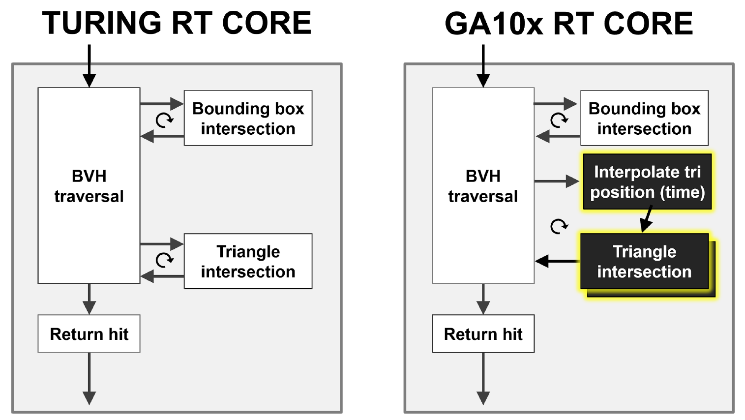
Figure 9. Comparison of hardware acceleration of motion blur in the case of Turing and Ampere
The main problem with motion blur is that the triangles in the scene are not fixed in time. In basic ray tracing, static intersection tests are performed, and when a ray hits a triangle, it returns information about that hit. As shown in Figure 10, with motion blur, none of the triangles have fixed coordinates. Each ray is timestamped to indicate its tracking time, and the position of the triangle and the intersection of the ray is determined from the BVH equation.
If this process is not accelerated by hardware, it can really cause a lot of problems, including due to its nonlinearity.
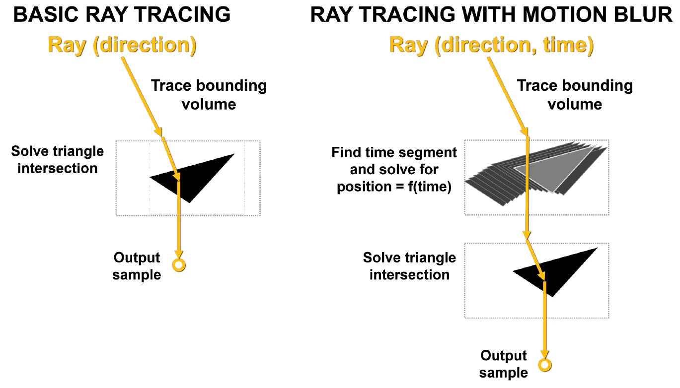
Drawing. 10. Basic ray tracing and ray tracing with motion blur
On the left side of Figure 11, rays sent to a static scene hit the same triangle at the same time. White dots show the place of hit, this result is returned back. In the case of motion blur, each ray exists at its own moment in time. Each beam is randomly assigned a different time stamp. For example, the orange rays try to cross the orange triangles at the same time, and then the green and blue rays do the same thing. At the end, the samples are blended, producing a more mathematically correct blurry result.
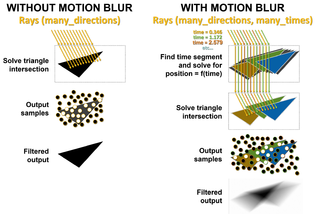
Figure 11. Rendering without motion blur and with blur in GA10x
The Interpolate Triangle Position block interpolates the triangles in BVH between the already existing triangles based on the movement of the object, so that the rays will intersect them at the expected locations at the moments specified by the ray timestamps. This approach allows accurate rendering of ray-traced motion blur up to eight times faster than Turing.
GA10x hardware accelerated motion blur is supported by Blender 2.90, Chaos V-Ray 5.0, Autodesk Arnold, and Redshift Renderer 3.0.X using the NVIDIA OptiX 7.0 API.
The rendering speed of motion blur is up to 5x faster on the RTX 3080 compared to the RTX 2080 Super.
3rd Generation Tensor Cores in GA10x GPUs
The GA10x includes new third-generation NVIDIA Tensor Cores, featuring support for new data types, improved performance, efficiency, and programming flexibility. The new sparsity feature doubles the performance of Tensor Cores over the previous generation Turing. AI functions such as NVIDIA DLSS for AI super-resolution (now with 8K support), NVIDIA Broadcast for voice and video processing, and NVIDIA Canvas for drawing are also faster.
Tensor kernels are specialized execution units designed to perform tensor / matrix operations - the main computational function in deep learning. They are needed to improve graphics quality with DLSS (Deep Learning Super Sampling), AI-based noise cancellation, removal of background noise inside game voice chats with RTX Voice, and many more applications.
The introduction of Tensor Cores into GeForce gaming GPUs has enabled real-time deep learning in gaming applications for the first time. The third generation tensor core design in GA10x GPUs further increases raw performance and leverages new computational precision modes such as TF32 and BFloat16. This plays a big role in AI-based NVIDIA NGX neural services applications to improve graphics, rendering and other features.
Comparison of Turing and Ampere Tensor Cores
Ampere Tensor Cores have been reorganized over Turing to improve efficiency and reduce power consumption. The Ampere SM core architecture has fewer tensor cores, but each one is more powerful.
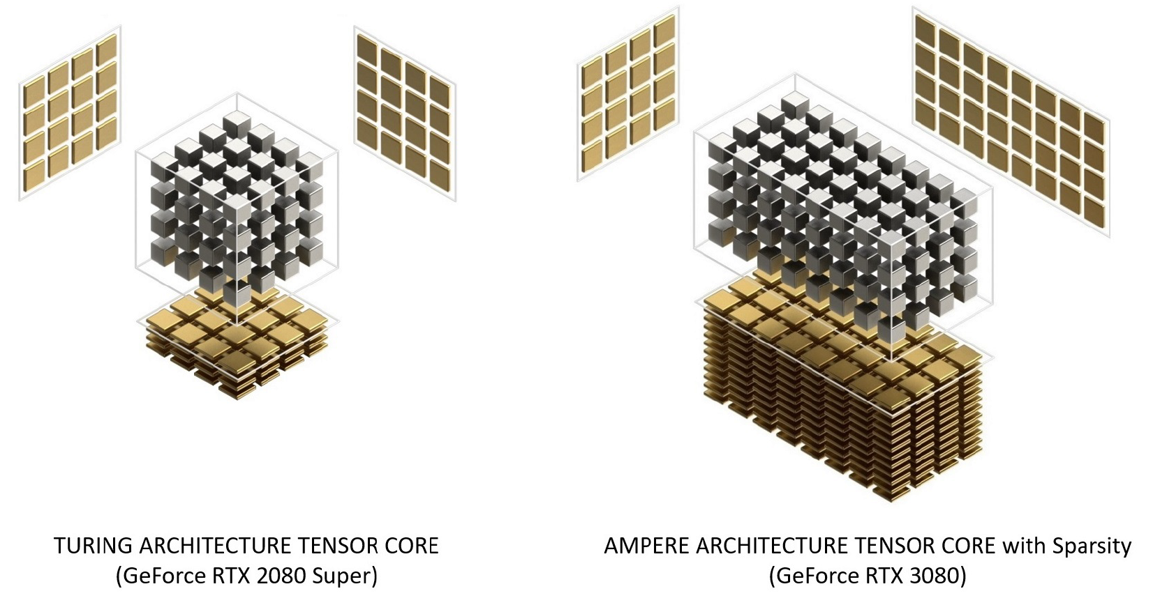
Figure 12. Tensor cores with Turing and Ampere architecture. GeForce RTX 3080 delivers 2.7x faster FP16 Tensor Core peak bandwidth than GeForce RTX 2080 Super
Fine-grained structured sparsity
With the A100 GPU, NVIDIA is introducing Fine-Grained Structured Sparsity, a new approach to doubling computational bandwidth for deep neural networks. This feature is also supported by GA10x GPUs and helps speed up some AI-based graphics rendering operations.
Since deep learning networks can adapt weights through feedback learning, in general, structural constraints do not affect the accuracy of trained models.
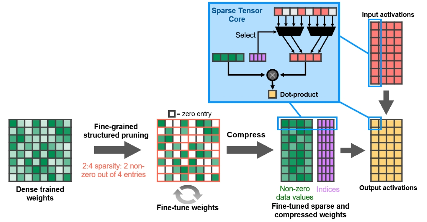
Figure 13. Fine-grained structured sparsity
NVIDIA has developed a simple and versatile deep neural network sparseness algorithm using a structured 2: 4 sparsity pattern. The network is first trained with dense weights, then fine-grained structured pruning occurs, after which zero values can be discarded, and the remaining mathematics is compressed to increase throughput. The algorithm does not affect the accuracy of the trained network for inference, it only speeds it up.
NVIDIA DLSS 8K
Rendering an image with ray tracing at a high frame rate is extremely computationally expensive. Prior to the advent of NVIDIA Turing, it was believed that its implementation would take years. To help solve this problem, NVIDIA has created Deep Learning Supersampling (DLSS).

Figure 14. Watch Dogs: Legion with DLSS at 1080p, 4K and 8K. Note the crisper text and detail provided by DLSS in 8K
DLSS is only getting better on the NVIDIA Ampere through the use of third-generation tensor cores and 9x super-resolution scaling factor, which for the first time makes it possible to run a ray-traced game at 8K at 60 fps.
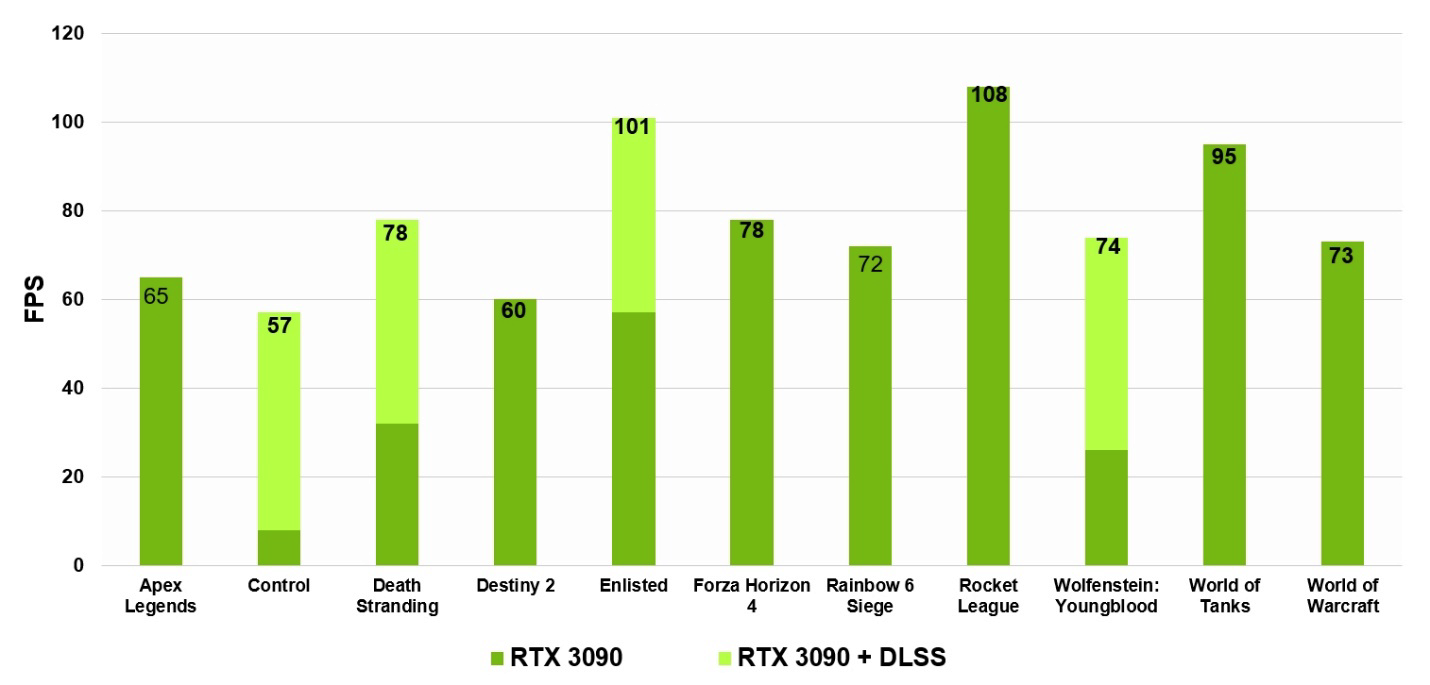
15. GeForce RTX 3090 60 fps 8K DLSS . , . Core i9-10900K
GDDR6X
Modern PC games and creative applications require significantly more memory bandwidth to handle increasingly complex scene geometry, more detailed textures, ray tracing, AI inference, and of course shading and supersampling.
GDDR6X is the first graphics memory to exceed 900 GB / s. To achieve this, innovative signaling technology and four-level pulse amplitude modulation (PAM4) have been employed, collectively revolutionizing the way data is moved in memory. With the PAM4 algorithm, GDDR6X transfers more data at a much faster rate, moving two bits of data at a time, which doubles the I / O data rate of the previous PAM2 / NRZ scheme.
GDDR6X currently supports 19.5 Gbps for the GeForce RTX 3090 and 19 Gbps for the GeForce RTX 3080. Thanks to this, the GeForce RTX 3080 offers 1.5 times the memory performance of its predecessor, the RTX 2080 Super. ...
Figure 16 shows a comparison of the structure of GDDR6 (left) and GDDR6X (right). GDDR6X transmits the same data at half the frequency of GDDR6. Or, alternatively, GDDR6X can double its effective bandwidth while maintaining the same frequency.

Figure 16. GDDR6X using PAM4 signals shows better performance and efficiency than GDDR6
To address the SNR problems encountered in PAM4 signaling, a new MTA (Maximum Transition Prevention) coding scheme has been developed. The MTA prevents high-speed signals from going from the highest to the lowest and vice versa.

Figure 17. New Encoding in GDDR6X
Supporting data rates up to 19.5 Gbps on GA10x chips, GDDR6X delivers peak memory bandwidth of up to 936 GB / s, 52% more than the TU102 GPU used in GeForce RTX 2080 Ti. GDDR6X has the biggest bandwidth jump in 10 years after GeForce 200 series GPUs.
RTX IO
Modern games contain huge worlds. With the development of technologies such as photogrammetry, they are increasingly imitating reality and, as a result, are contained in files with increasing volume. The largest gaming projects take up more than 200 GB, which is 3 times more than four years ago, and this number will only grow over time.
Gamers are increasingly turning to SSDs to reduce game load times: While hard drives are limited to 50-100MB / s bandwidth, the latest M.2 PCIe Gen4 SSDs read data at up to 7GB / s.
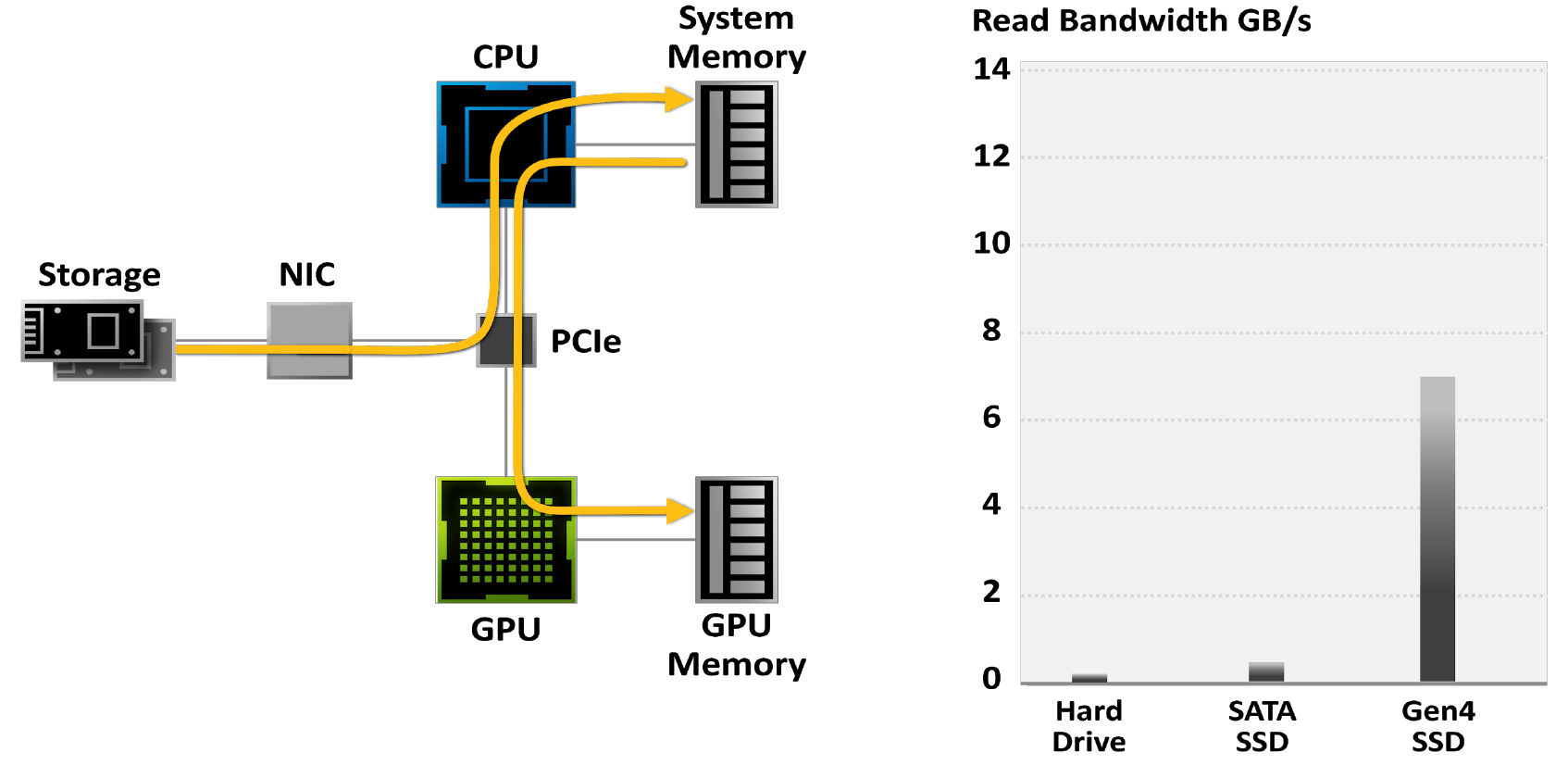
Figure 18. Games limited by traditional I / O systems

Figure 19. Using the traditional storage model, unpacking a game can take all 24 processor cores. Modern game engines have surpassed the capabilities of traditional storage APIs. This is why a new generation of I / O architecture is needed. Here, gray bars indicate the data transfer rate, black and blue blocks - the CPU cores required for this.
NVIDIA RTX IO is a set of technologies that provide fast loading and unpacking of GPU-based assets and deliver I / O performance up to 100x faster than hard drives and traditional storage APIs.
NVIDIA RTX IO is powered by the Microsoft DirectStorage API, next-generation storage designed specifically for today's NVMe SSD gaming PCs. NVIDIA RTX IO delivers lossless decompression, allowing data to be read in compressed form via DirectStorage and delivered to the GPU. This offloads the CPU load by moving data from storage to the GPU in a more efficient compressed form and doubling I / O performance.

Figure 20. RTX IO Delivers 100X More Throughput and 20X Lower CPU Usage. Gray and green bars indicate the baud rate, black and blue blocks are required for this CPU core.
Display and video engine
DisplayPort 1.4a with DSC 1.2a
The march towards ever higher resolutions and higher frame rates continues, and NVIDIA Ampere GPUs are striving to stay at the forefront of the industry to deliver both. Gamers can now play on 4K (3820 x 2160) displays at 120Hz and 8K (7680 x 4320) at 60Hz - four times the pixel count of 4K.
The Ampere architecture engine is designed to support many of the new technologies included in the fastest display interfaces available today. This includes DisplayPort 1.4a, which delivers 8K @ 60Hz with VESA Display Stream Compression (DSC) 1.2a. The new Ampere GPUs can be connected to two 8K 60Hz displays with just one cable per display.
HDMI 2.1 with DSC 1.2a
The NVIDIA Ampere architecture adds support for HDMI 2.1, the latest update to the HDMI specification, for the first time for discrete GPUs. HDMI has increased the maximum bandwidth to 48 Gbps, which also allows for dynamic HDR formats. Support for 8K @ 60Hz with HDR requires DSC 1.2a compression or 4: 2: 0 pixel format.
5th Generation NVDEC - Hardware Accelerated Video Decoding
NVIDIA GPUs include 5th Generation Hardware-Accelerated Video Decoding (NVDEC), which provides full hardware video decoding for a variety of popular codecs.

Figure 21. Video encoding and decoding formats supported by GA10x
GPUs The fifth generation NVIDIA decoder in GA10x supports hardware accelerated decoding of the following video codecs on Windows and Linux platforms: MPEG-2, VC-1, H.264 (AVCHD), H.265 (HEVC), VP8, VP9, and AV1.
NVIDIA is the first GPU manufacturer to provide hardware support for AV1 decoding.
AV1 hardware decoding
Although AV1 is very efficient at compressing video, decoding it is computationally intensive. Modern software decoders cause high CPU utilization and make it difficult to play ultra-high definition video. In NVIDIA tests, the Intel i9 9900K processor averaged 28 frames per second on YouTube in 8K60 HDR, with CPU utilization exceeding 85%. GA10x GPUs can play AV1 by passing decoding to NVDEC, which is capable of playing up to 8K60 HDR content with very low CPU usage (~ 4% on the same CPU as in the previous test).
7th Generation NVENC - Hardware Accelerated Video Encoding
Video encoding can be a complex computational task, but if you upload it to NVENC, the graphics engine and CPU are freed up for other operations. For example, when streaming games to Twitch.tv using Open Broadcaster Software (OBS), offloading video encoding to NVENC will allocate the GPU's graphics engine for rendering the game, and the CPU for other user tasks.
NVENC allows:
- High quality ultra-low latency encoding and streaming of games and applications without using the CPU;
- very high quality encoding for archiving, OTT streaming, web video;
- Ultra-low power encoding per stream (W / stream).
With shared streaming settings for Twitch and YouTube, NVENC-based hardware encoding in GA10x GPUs outperforms x264 software encoders using the Fast preset and is on par with x264 Medium, a preset that typically requires the power of two computers. This drastically takes the load off the CPU. 4K encoding is too much workload for a typical CPU configuration, but the GA10x NVENC encoder provides seamless high-resolution encoding up to 4K in H.264 and even 8K in HEVC.
Conclusion
With each new processor architecture, NVIDIA strives to deliver revolutionary performance to the next generation while introducing new features that improve image quality. Turing was the first GPU to introduce hardware-accelerated ray tracing, a feature once considered the holy grail of computer graphics. Today, incredibly realistic and physically accurate ray tracing effects are being added to many new AAA PC games, and GPU-accelerated ray tracing is considered a must-have feature for most PC gamers. The new NVIDIA GA10x Ampere GPUs deliver the features and performance you need to enjoy these new ray-traced games with up to 2x faster frame rates than currently available.Another feature of Turing - improved CPU-accelerated AI processing that improves noise cancellation, rendering and other graphics applications - is also taken to the next level thanks to the Ampere architecture.
Finally, a link to the full document .