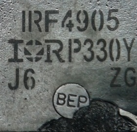
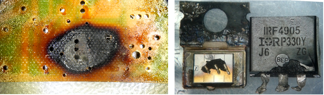
On the board of some device N, the IRF4905 transistor burned out, so much so that it cracked, so it became possible to look at its internal structure.
IRF4905 characteristics according to the documentation: P-channel field-effect transistor. Direct current at 20 C - 74 A, pulsating current up to 260 A. On-state resistance - 0.02 Ohm. Low resistance is achieved by the HEXFET technology, the essence of which is that a field-effect transistor is not one transistor, but many (hundreds of thousands) of small field-effect transistors connected in parallel.
The maximum power dissipation of the transistor is 200 W. As proof of such great indicators - a burnt-out textolite and a cracked transistor (it was held to the last).
The crystal itself has an area of 24 mm2. Crystal thickness 0.3 mm. Soldered on eutectic.
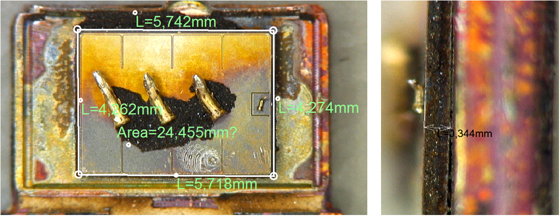
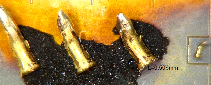
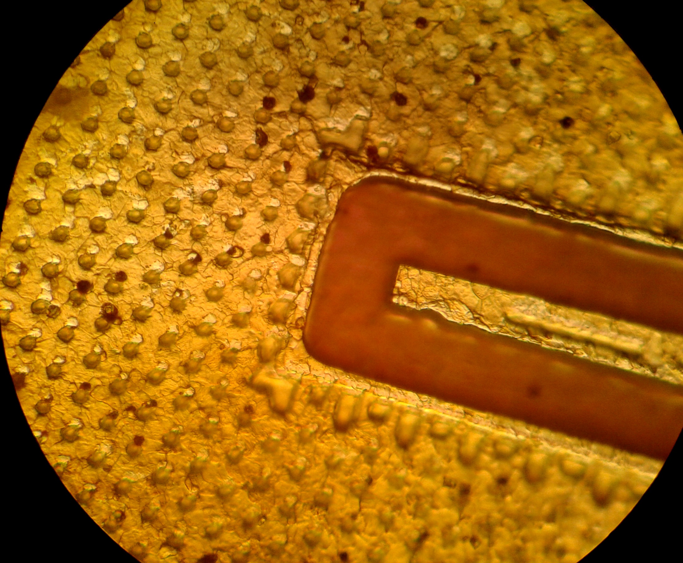
Welding is done with aluminum wire. A yellowish bloom is visible on it - this is carbon deposits. The control electrode has a diameter of about 50 μm, and three thick wires with a diameter of 0.5 mm each. The thick wire shows a trace from the welding tool.
Schematically, the HEXFET technology by International Rectifier looks like this:
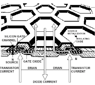
According to the documentation, the IRF4905 transistor is implemented on the fifth generation of HEXFET technology.
Photos can be opened in a new window and viewed in more detail. With each photo, you get closer to understand the scale of the dive.
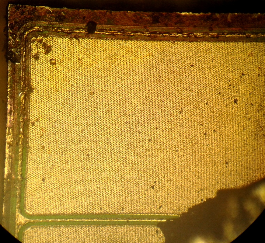
~ 100X zoom
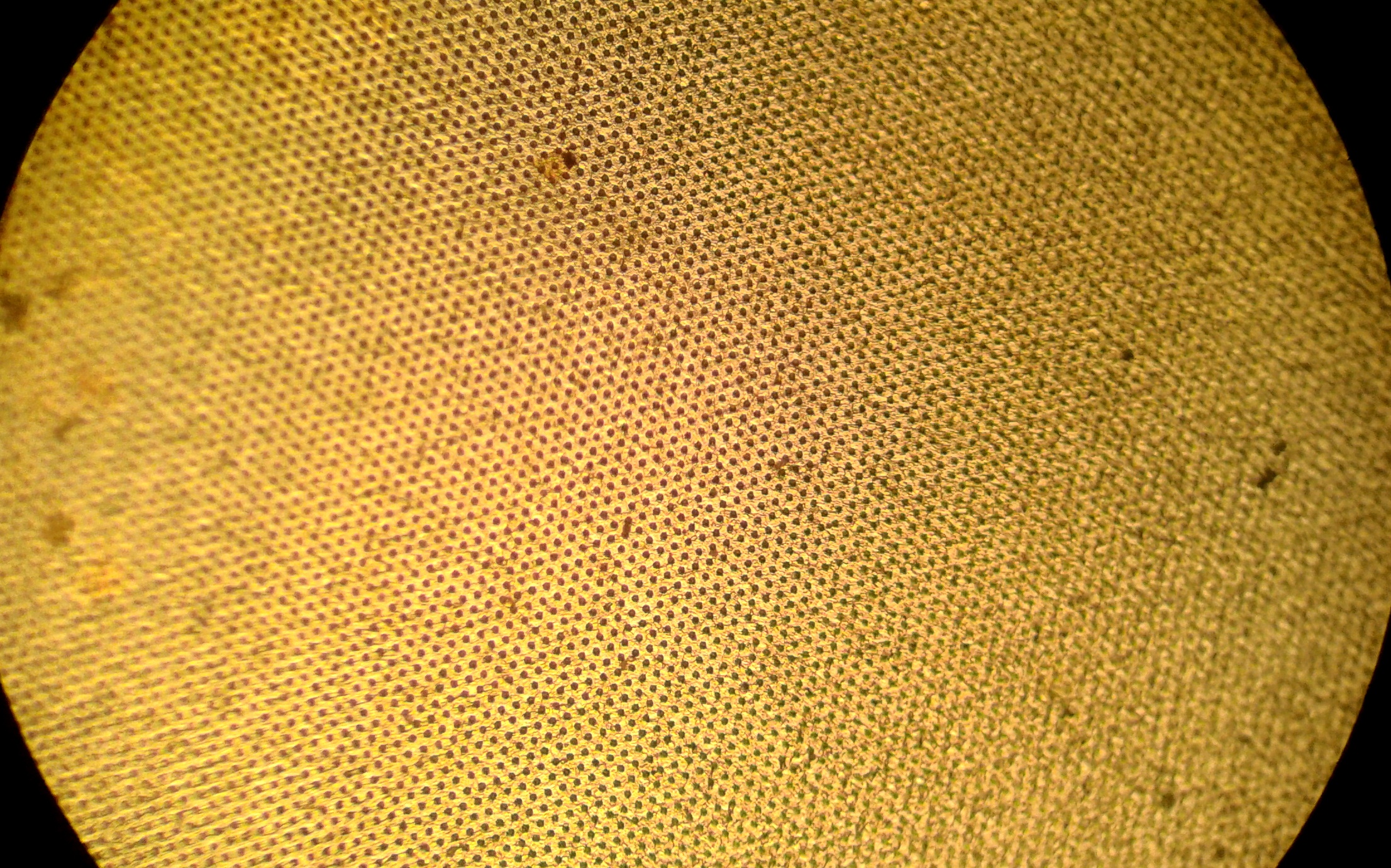
~ 200x approximation
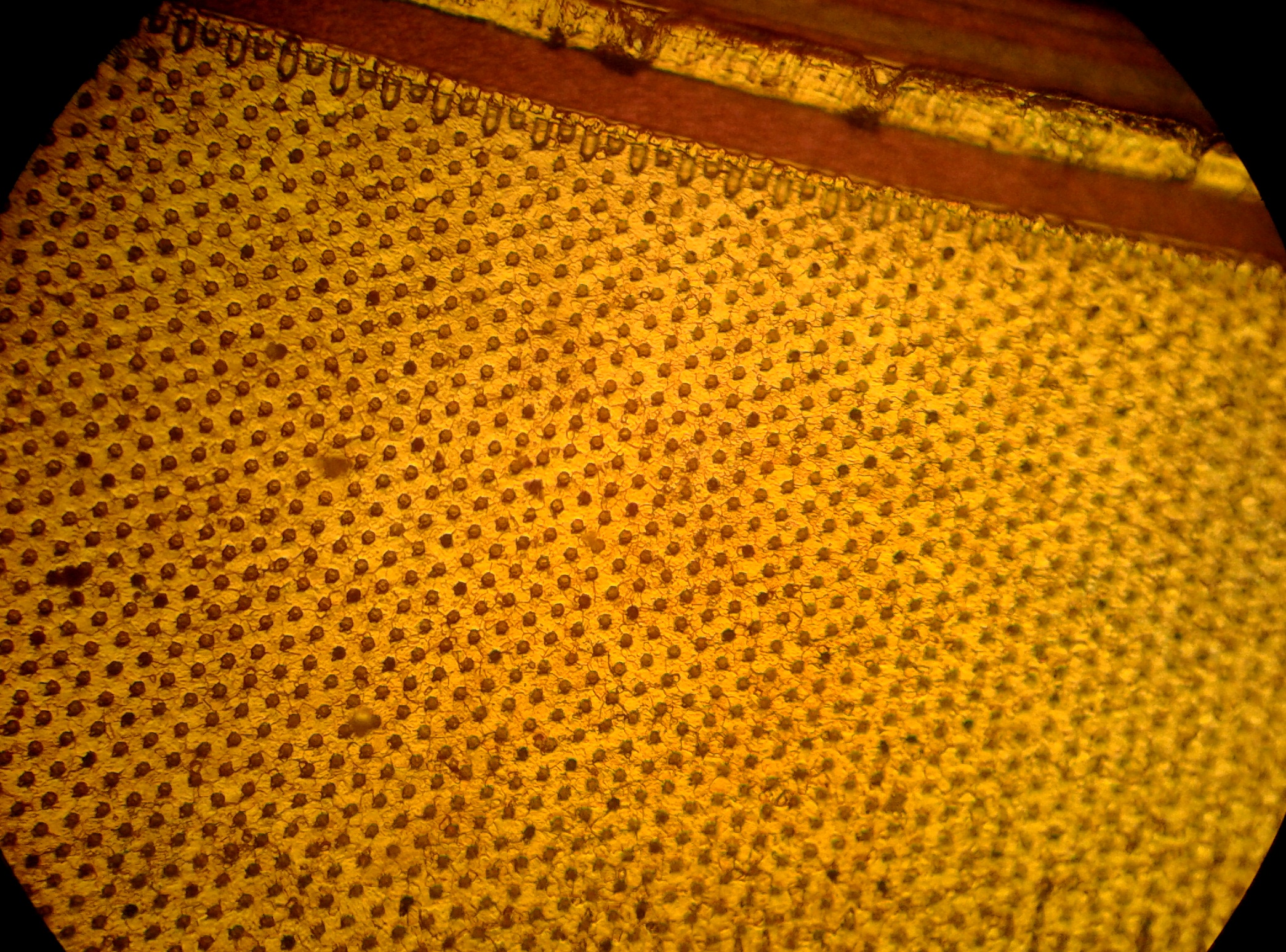
~ 400 X approximation
~ 1000x approximation
This is what the top topology of the FET matrix looks like.
I tried to bleed off the top metallization layer with ammonium persulfate. It turned out to be dirty, but the clear contours of the hexagonal shape became visible. The approximate dimensions of the hexagons are 5-7 microns (this is 5000-7000 nm).

Thank you for attention.