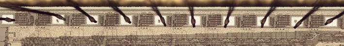
The photo below shows an 8086 crystal under a microscope. A metal layer is visible on top of the chip, under which a silicon substrate and a polysilicon layer with conductors are hidden. Along the outside of the perimeter of the crystal, a tiny wire bond connects the pads of the crystal to the outer legs. On the 8086, the power pad is on top and the ground pads are on top and bottom. Each of them has two wires for welding wires, which doubles the current supported. Wide metal paths are visible extending from the power and ground pads. They distribute power across the chip.
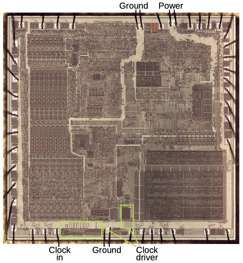
Photo of the 8086 crystal, where you can see the power supply point (top) and ground contacts (top and bottom). The timing circuits are located at the bottom.
There are two internal clock signals responsible for synchronization in the 8086. An external oscillator feeds clock signals to the 8086 through the input clock pad below. The internal clock generator provides two high-current clock signals based on external signals. Note that the clock driver takes up a large footprint on the chip.
In this article, I will describe how the 8086 redirects energy and clock signals throughout the chip, and how the clock circuitry generates the necessary clock pulses.
Power distribution
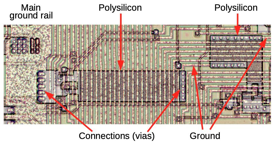
8086 consists of three layers, each of which can accommodate conductors. The metal layer on top is best for this due to the low resistance of the metal. Under the metal there is a polysilicon layer of conductors, consisting of a special type of silicon. The resistance of polysilicon is higher than that of metal, but it can still be used to transmit signals across the chip. Transistors are formed on the silicon substrate. The resistance of silicon is relatively high, so it is only used to transmit signals over short distances - for example, inside a gate.
The distribution of power in a chip like the 8086 is a topological puzzle. Due to its low resistance, the metal layer remains the only practically useful layer for power and ground wiring. Almost all gates on the chip must be supplied with power and ground. And since the chip has one metal layer, power and ground cannot intersect.
Nearly all gates on the chip need power and ground because the standard MOS gate requires ground for its pull-down network and power for its pull-up resistor. However, there are a few exceptions. 8086 uses dynamic logic gates, especially in ALU - for speed. These gates are attracted upward by the sync signal, so they do not need a direct power supply. The 8086 also uses multiple XOR gates at the feed-through transistors, which are pulled down by the incoming signal, so they don't need ground.
The microcode ROM forms a large section of the chip that does not need power, only ground. This is because each row of ROM is implemented as a very large NOR gate, and the power that pulls it up is located on the right edge. Therefore, all ROM gates have power and ground, although it seems that the ROM lacks a power connection.
The diagram below shows the metal conductors in the 8086. The power supply connected to the power pin on top is shown in red. A powerful branch of the food goes down and to the right, and then divides into many branches. Power also runs along the edge of the entire chip, providing power to the I / O pins.
With ICs, it often happens that the power and ground are located in opposite corners or on opposite sides of the chip. This arrangement makes it easier to route the power and ground tracks that do not cross each other. The 8086 has a slightly unusual positioning of power and ground on diagonally opposite pins, and the second ground closer to the power pin. The power networks and the lands on the chip branch out like trees. These networks branch out and, like intertwined fingers, reach all parts of the chip.
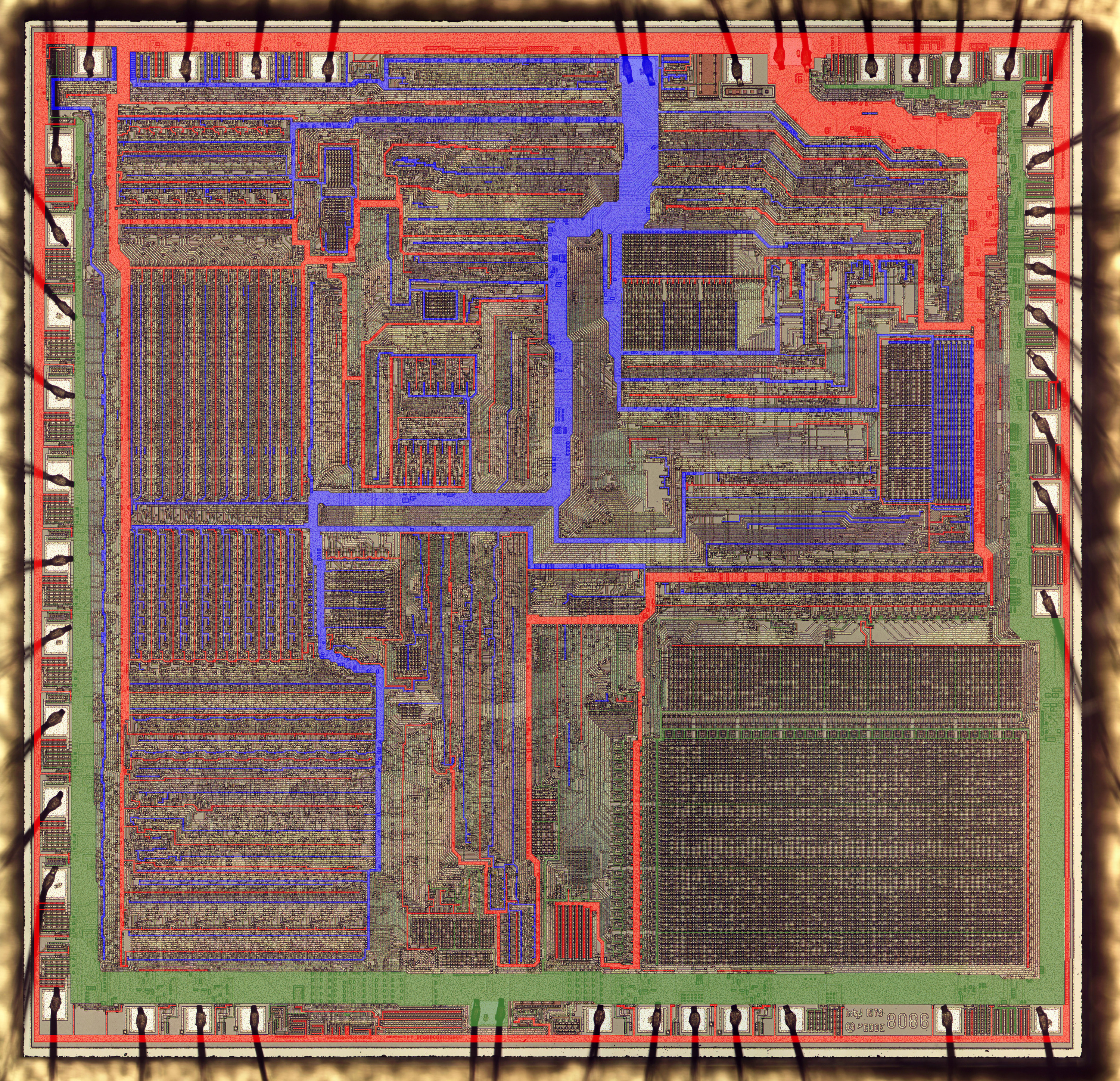
Power (red) and ground (blue, green) on the metal layer of the chip
There are two ground contacts. The tracks marked in blue connect to the top ground pin, and the green ones to the bottom. The blue marked ground paths show a thick branching down through the center of the chip and branching out in an intricate way in all directions. The green lanes run along the bottom, left and right sides of the chip, supporting the I / O pins as well as connecting to the microcode ROM at the bottom right.
Moving further away from the power source and getting closer to the end points, the power conductors become thinner and the current decreases. This can be seen in the power conductor to the address and data pins below. On the left under the contacts, the conductor with the ground is very wide, but it gradually narrows, going to the right. In other words, on the left, the conductor must conduct current from all contacts, and on the very right side, only from one.
The connection of the address and data pins to ground is getting thinner (left side of the chip rotated 90 °) The
metal layer is used to carry many signals, not just power and ground. Because of its low impedance, it is the best signal transmission layer. However, the widespread use of power and ground conductors limits the capabilities of the metal layer. To avoid crossover, most of the signal paths on the metal layer run parallel to the power paths. A layer of polysilicon underneath is used for perpendicular signal transmission. But what happens if a metal conductor needs to cross a power or ground track? The solution is to draw it from the bottom [crossunder]. The signal descends to the polysilicon level, crosses the track, and then rises back up as shown below.
Such bottom crossings are used in many cases, not only with food. However, most often it is about nutrition. Typically, metallic conductors are used to transmit signals in one direction, and polysilicon conductors are used to transmit signals in the perpendicular direction. In different places on the chip, these directions change, and depend on the dominant direction of signal transmission. Therefore, for the most part, signals travel unhindered. And yet they often have to jump from layer to layer.
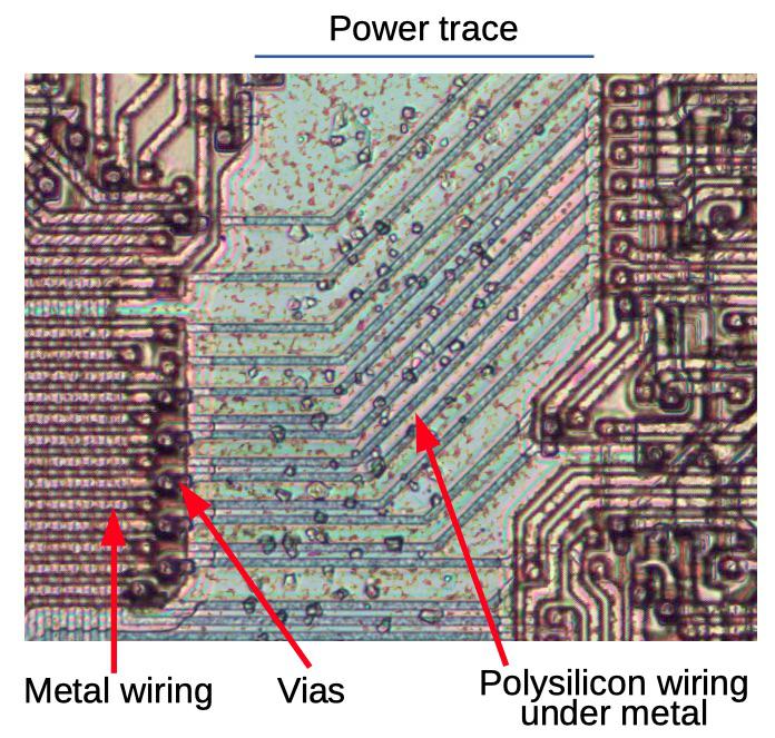
Signals on the metal layer traverse the supply paths from below via a polysilicon layer
If the power and ground are almost entirely routed to the metal layer, in a couple of places this circuit is broken, and the tracks passing through the bottom are used to supply power. This happens more often in the very last sections of the tracks, where the current is already low. One example is shown below - where the ground passes twice from the bottom of the metal layer using polysilicon conductors. To reduce resistance, these bypass paths are made much wider than the signal paths and also use silicon and polysilicon together. Small circles are through contacts [via] between the metal and polysilicon layers.
Composite photo showing ground bypass paths running through polysilicon under the signal paths.
The silicon layer plays a minor role in power wiring. In particular, many gates are stretched to reach power and ground from the other side. The photo below shows the 8086 gates. Note the large areas of doped silicon (white) that are pulled out to reach the ground and power rails. Only a small fraction of the silicon is used for transistors, and everything else seems like a waste of space. However, these empty sections of silicon connect the gates to metal conductors that supply power and ground. Since silicon has a relatively high resistance, wide areas are used for this, and the joints themselves extend over short distances.
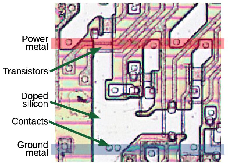
The gates made with doped silicon can be extended to reach the power and ground rails. For this photo, the metal layer has been removed.
After the 8086 was updated and physically shrunk, it had other power wiring issues. With the improvement of manufacturing technology, Intel scaled the crystals - left the circuits the same, but reduced them proportionally. Unfortunately, reducing the size of the power supply tracks also reduces the maximum current. To solve this problem, the power paths around the chip were reinforced and the internal circuitry and wiring reduced. This can be seen in the photo below - for example, there are many more power tracks in the lower right corner of the smaller 8086.
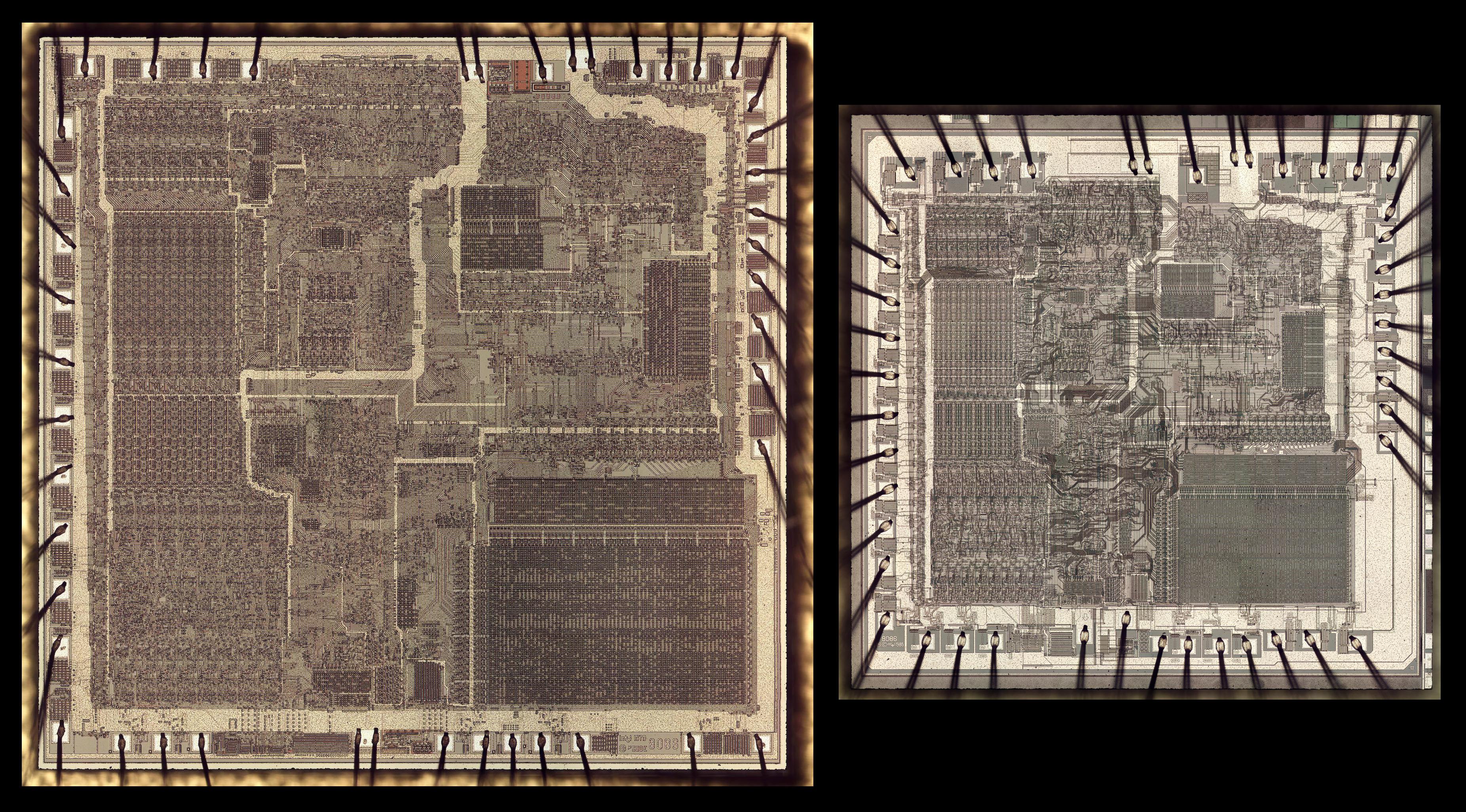
Two versions of 8086 on the same scale. The crystal on the right is a later version, reduced in size.
Almost all computers use clock signals to control the timing of the processor. The 8086, like many microprocessors, uses a two-phase clock driver internally. A two-phase clock driver has two clocks - when the first is high, the second is low, and vice versa, as shown below. Some circuits are turned on with the first sync signal, and others with the second. The scheme of operation of the 8086 implies that there is no overlap between the two phases of the sync signals and their asymmetry - there is a gap between the moments when one sync signal becomes low and the second rises.
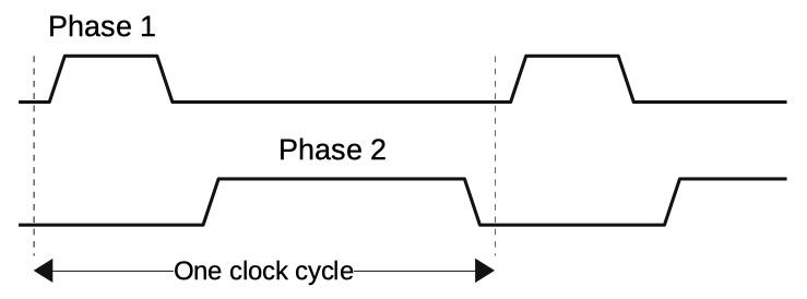
A two-phase clock driver consists of two clock signals of opposite polarity
Although almost all computers use clock signals for synchronization, the machineThe IAS architecture (popular in the 1950s) was asynchronous, and operated without clock signals. Instead, each circuit, when finished, sent a pulse to the next, triggering the next step. Many of the early 1950s computers were based on this architecture, including CYCLONE, ILLIAC, JOHNNIAC, MANIAC, SEAC, and the IBM 701. Research into the possibilities of asynchronous computing continues , but synchronous systems certainly dominate.
Processors, among other things, use clock signals to prevent unwanted feedback in the circuits. For example, consider a software counter whose chain increments its value and feeds it back to the counter. You don't want the new value to keep increasing.
One method is to use triggers that update the value when the signal goes from low to high. Then the counter will be updated the only time, which is required. However, with a two-phase sync signal, the circuit can be made on level-sensitive latches, the design of which is much simpler than for triggers that are sensitive to signal changes. When the first sync signal is high, the first half of the rung receives an input value and performs logical calculations. When the second sync signal is high, the second part of the chain receives the result from the first half and performs all the necessary calculations, and the first part is blocked. The point is that only half of the chain can be updated at a time, which prevents unwanted feedback.
The 8086 has strict input clock requirements, which must be high for a third of the time. Typically, the 8086 was generated by the 8284 chip and a quartz crystal. The chip divided the incoming clock signal by 3 to provide the 33% clock duty cycle required by the 8086.
In modern processors, the clock signal layout is very complex because the signal must travel to all parts of the chip simultaneously. Modern processors use a hierarchy of clock paths, balance the travel times along each path, and often provide separate buffering for each path. For comparison, the 8086's clock signal layout is straightforward, since its clock frequency of 5-10 MHz is several orders of magnitude lower than that of modern processors. At these relatively low frequencies, the path length doesn't really matter, so the 8086's clock pulses can follow winding paths.
Since the 8086 used dynamic logic, it also had a minimum clock speed of 2 MHz. If the frequency is lower, there is a risk of charge leakage before the charge is renewed, which can lead to failures. The minimum clock frequency was inconvenient from a debugging point of view, since it was impossible to slow down or stop the clock signal.

Sync paths in the 8086. Green is the first sync and red is the second, with opposite phase
The diagram above shows the 8086's clock paths. Phase 1 is green and phase 2 is red. At the bottom of the chip, the clock driver circuits appear as large spots. From there, the sync signals branch out across the entire chip. For the most part, the two clock phases run in parallel, as opposed to power and ground with their opposite branches.
Since the sync signals travel to all parts of the chip, they require much more current than conventional signals, and therefore they are mostly routed to the metal layer. When the sync signals need to cross the power tracks, they pass underneath them, as shown below. Note that sync workarounds are irregular in shape - they are much more than workarounds for other signals, such as the Q bus.
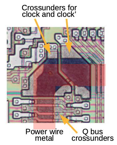
The bypass paths of the power supply are quite large. The Q bus (transmitting command from the command queue to the decoder) has much less.
To provide high-current sync signals, their shaper circuit is built on large transistors. The photo below compares one of these transistors with a typical logic transistor. The driver transistors are about 300 times larger, so it is capable of delivering about 300 times the current. The transistor is made up of 10 transistors placed in parallel - 10 vertical polysilicon lines form 10 gates. Each sync signal is generated by a pair of large transistors, one of which pulls it up and the other down.

Large transistor in the clock driver compared to the adjacent logic transistor
The photo below shows the schematic of the sync pulse generator. The circuit splits the external clock signal into two phases, ensures that they do not overlap, and amplifies them. The pink square on the left is a platform for an external clock driver. The signal travels through a series of transistors ending in the large driver transistors on the right side. The brown conductors are polysilicon forming the gates. Many transistors have zig-zag gates so that a large transistor fits in a small space.
On-chip clock driver circuit. The metal layer has been removed. Large transistors are visible. External sync input pin - pink square on the left.
Below is a slightly simplified schematic diagram of the synchronizing pulse generator. Triangles are high-current drivers made of two or three transistors. The inverting input (circle) pulls the output down. On the left side of the input sync pin, there is a small resistor and diode that protects it (just like the other input pins). The sync signal is then split into phase inverted (top) and phase inverted (bottom).
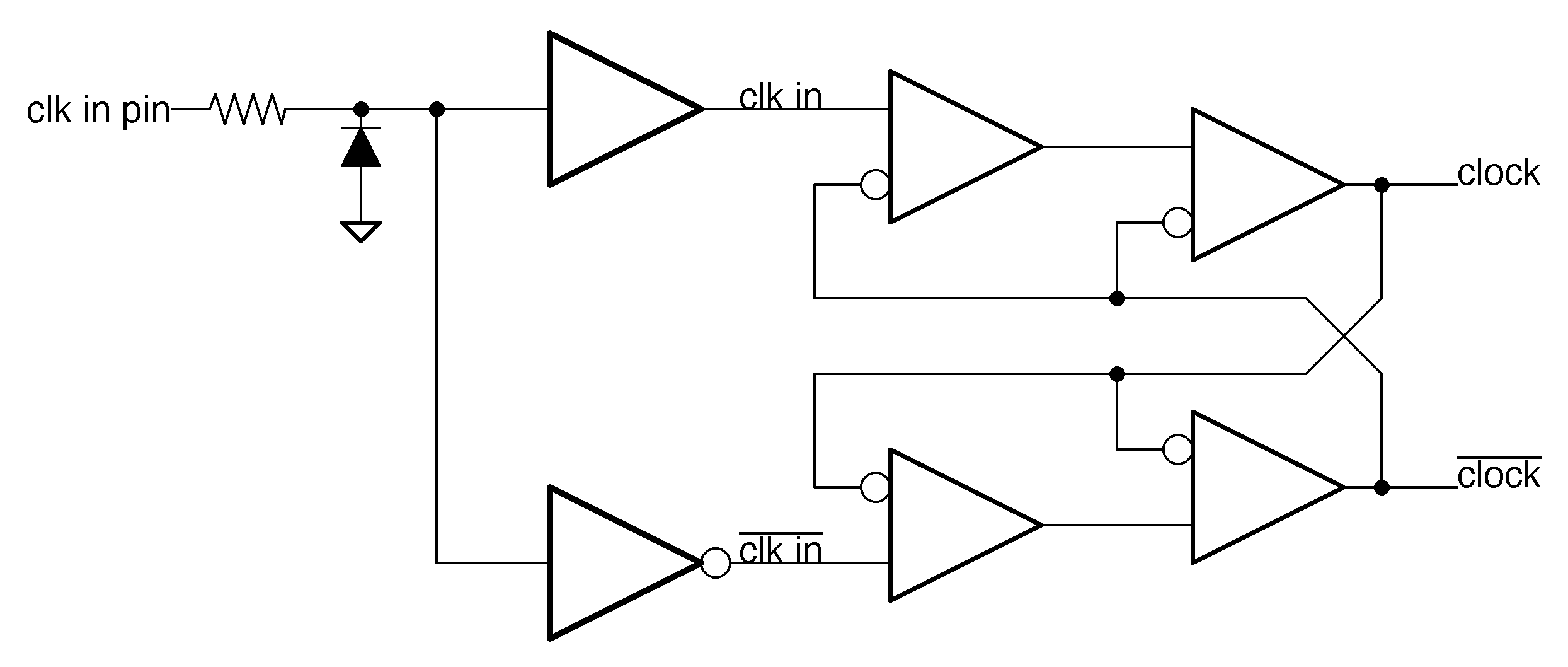
Simplified schematic diagram of the 8086 clock generator
Additional circuits prevent sync signals from overlapping: when one signal is high, this, through an inverted input, causes the second signal to be low. To understand how this works, let's start with the moment when the signal on the clk in pin is high. The signals clk in and clock are high, while ^ clk in ^ and ^ clock ^ are low. Now, let's say the incoming signal to clk in goes low, which causes the signal to clk in to go down and on ^ clk in ^ to go up. However, the output of ^ clock ^ cannot go up until clock goes down. After that, the signal ^ clk in ^ will go through the lower drivers, pulling ^ clock ^ up after two gate delays. The point is that clock and ^ clock ^ do not switch at the same time. After one goes low, there is a delay before the other goes high.As a result, we get non-overlapping sync signals.
This is a pretty rough description - in particular, I'm not sure what happens when one transistor pulls a signal up and another pulls the same signal down. The exact simulation of the process will depend on the relative sizes of the two transistors.
Conclusion
The 8086 uses an interesting power layout, but modern processors operate on a completely different level. If the 8086 required 350mA, then a modern processor may need more than 100A. The 8086 used 3 of its 40 legs for power and ground. Modern Intel Core i5 processors have 128 power pins and 377 - ground (out of a total of 1151 pins). While the numerous metal layers in modern chips solve the 8086's wiring problems, they introduce new complications such as dividing the chip into power sections, which allows you to turn off unused sections.
In modern processors with their multi-gigahertz speeds, the wiring of sync signals is much more complicated, because an extra millimeter of track can negatively affect the sync signal. To solve these problems, modern processors use things like H-trees or clock distribution networks, rather than just branching tracks like the 8086. Whereas the 8086 had a simple two-phase clock generating circuit, modern processors often use phase locked loop to synthesize the clock signal. , and many circuits scattered throughout the chip that provide and control clock signals. But while the 8086 is much simpler than modern processors, it contains many examples of interesting circuits.