The 8086 has over 80 latches. Some of them store the values of AD pins (address / data) or control pins. Others store the current address of the microcode and microcode, as well as the return address from the microcode routine. The third stores the bits of the source and output command register, and the ALU-operation of the command. Many store the statuses of the internal state, which I still understand.
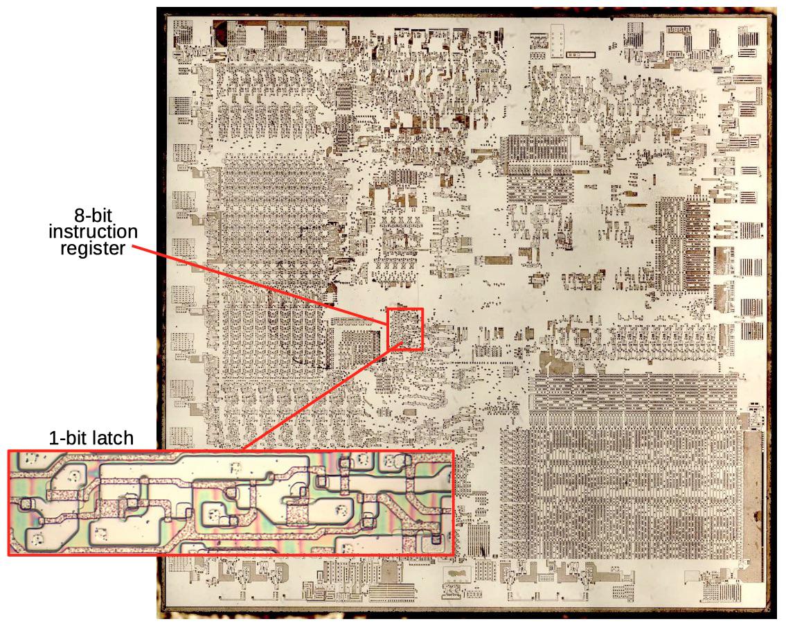
Crystal 86 showing the 8-bit instruction register
The photo above shows the 8086 silicon die under a microscope. I removed the metal and polysilicon layers so that you can see the transistors - there are about 29,000 in total. The allocated area contains an 8-bit command buffer, consisting of eight latches. This 1978 processor was still simple enough for a single 8-bit register to take up a relatively large area. The magnification shows silicon and transistors that make up a single latch.
How a dynamic latch works
The latch is one of the most important elements of the 8086, as latches keep track of what the processor is doing. Latches can be done in different ways; the 8086 uses a compact circuit known as a dynamic latch. The dynamic latch relies on the operation of a two-phase clock generator, which was often used to control microprocessors of that era. The two-phase clock generates two clock signals that are active in turn. In the first phase, the main clock is high and the accompanying clock is low. Then they change places. The cycle is repeated at a clock frequency, for example 5 MHz.
Many microprocessors use NAND gates to form RS flip-flops. An RS flip-flop usually takes up more space than a dynamic latch, especially if additional circuits are added to it to maintain the clock frequency. D-triggers (delay triggers) are also popular, but they get even more complex and use six gates. In many cases, a pass transistor is sufficient; it can store a value for one clock cycle, but does not provide long-term storage.
The highest possible clock speed is always chosen for processors. The first 8086 worked at up to 5 MHz, and later the 8086-1 supported up to 10 MHz. However, due to the use of dynamic logic, the 8086 also has a minimum clock frequency: 2 MHz. If the clock generator runs slower, there is a risk of charge leakage from the conductors before the circuits access it, leading to errors.
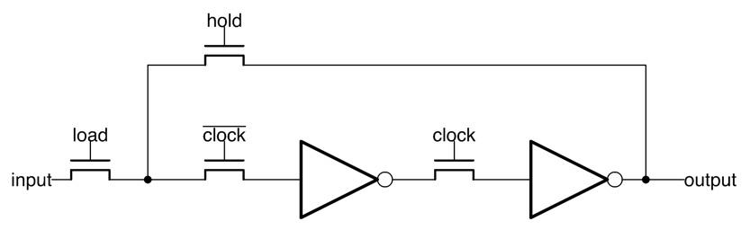
The latch in the 8086 processor consists of four pass transistors and two inverters. The latch operates on intermittent clock signals.
The diagram above shows a typical 8086 latch. It consists of two inverters and several pass transistors. For our purposes, the pass transistor can be considered a switch: if 1 comes to the gate, the transistor transmits the signal further. If 0 comes, the transistor blocks the signal. The pass transistor is controlled by several signals: load, which loads a bit into the latch; hold (hold), holding the existing bit value; the clock of the first phase and the clock of the second, inverted.
The diagram below shows how a value (in this case, 1) is loaded into the latch. The load signal rises, allowing the input signal (1) to pass through the transistor. Since the clock signalhigh, the signal passes through the second transistor to the inverter, which outputs 0. At this moment, the third (clock) transistor blocks the signal.
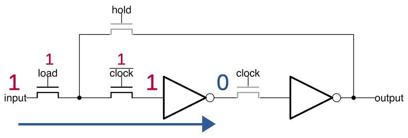
The input signal is loaded into the latch when the load signal is high
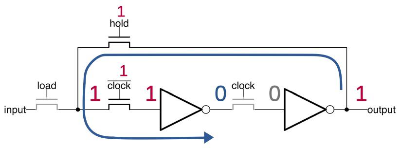
In the next clock phase, the clock signal goes high, causing the 0 signal to reach the second inverter, which outputs 1. Since the hold signal is high, the signal goes back but is blocked by the clock transistor... What makes this circuit dynamic is that no input signals are currently being sent to the first inverter. Its input remains 1 (shown in gray) due to the capacitance of the circuit. Someday this charge will leak, the value will be lost, but before that moment a new switching of the clock pulse generator will occur.

When the clock signal goes high, the value passes through the second inverter. The input to the first inverter (gray) is maintained by the capacitance of the circuit.
After switching the state of the clock generator, the input to the second inverter will provide the circuit capacity (see below). The signal is fed back, recharging and updating the input to the first inverter. On subsequent clock switches, the latch will toggle between this and the previous pattern, maintaining the stored value and keeping the output stable.
The key to the operation of the latch is the presence of two inverters, which keep the output signal stable. An odd number of inverters would cause oscillation - this feature is used by the 8086 charge pump. Also, a pair of inverters uses a set of 8086 registers to store bits. However, in a set of registers, the two inverters are directly connected, without the clock-driven pass transistors, resulting in a more compact but difficult to manage storage system.
When the clock signal is high, the value passes through the first inverter.
Implementation in silicon
The 8086 and other processors of that era were based on N-MOS transistors . They were made from a silicon substrate, to which arsenic or boron impurities were added during the doping process , which formed the transistors. On top of the silicon was polysilicon, which created the gates of the transistors and the conductors that connected all the components together. Another layer, metal, provided additional conductive connections. Modern processors, by comparison, use CMOS technology , a combination of N-MOS and P-MOS technologies, and they have more than one metallic conductive layer.
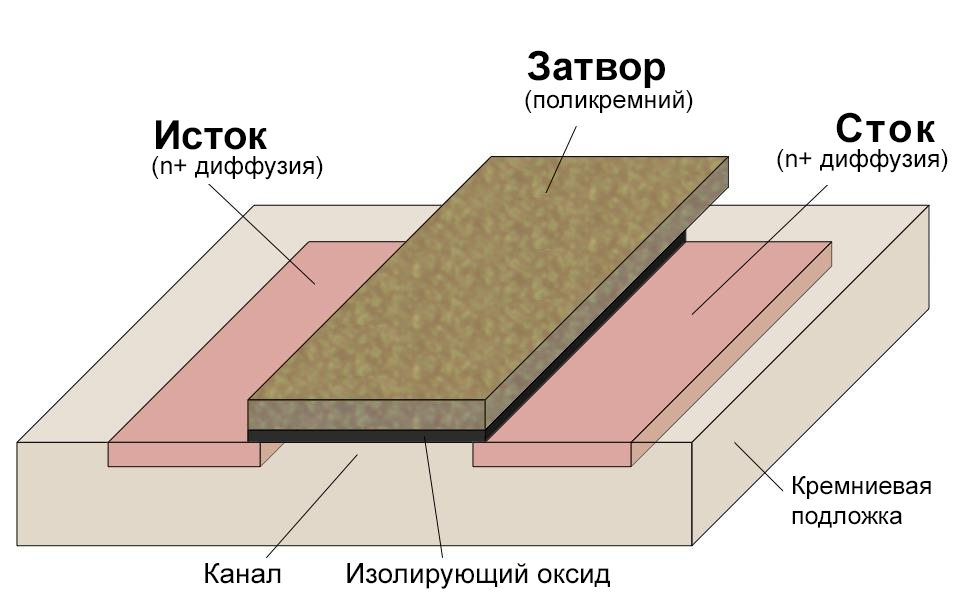
How an N-MOS transistor ( MOS structure ) is implemented in an IC
The diagram above shows the structure of the transistor. A transistor can be thought of as a switch that allows current to flow from one section (source) to another (drain). The transistor is driven by a gate made of a special type of silicon - polysilicon. Applying a voltage to the gate allows current to flow between the source and drain, while pulling the gate to 0 V blocks the current. The gate is separated from silicon by an insulating oxide layer - because of this, the gate works like a capacitor, as can be seen in the example of a dynamic latch.
The inverter (below) is made up of an N-MOS transistor and a resistor. When the signal is low, the transistor is off, so the pull-up resistor pulls the output signal up. When the signal is high, the transistor turns on, connecting the output to ground and pulling the output down. Thus, the circuit inverts the input signal.
The pull-up resistor in the N-MOS gate is implemented using a special type of transistor. A depletion-mode transistor works like a resistor but takes up less space and is more efficient.
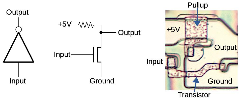
The diagram shows how an inverter is made from a transistor and a resistor. The photo shows how the circuit is implemented on the chip. The metal layer has been removed to reveal polysilicon and silicon.
The photo on the right shows how the 8086 physically implements an inverter. The yellowish areas are conductive silicon with impurities, and the spotty areas are polysilicon on top. The transistor is made where the polysilicon crosses the doped silicon. Polysilicon forms the gate of the transistor, and sections of silicon on both sides provide the source and drain of the transistor. A large polysilicon rectangle forms a pull-up resistor between + 5V and the output. You can compare the structure of these physical structures with a diagram.
The diagram below shows the implementation of the latch on the chip. A pass-through transistor and two inverters are marked; the first inverter is described above. Polysilicon conductors connect components to each other. Additional connections were provided by a metal layer (removed for the photo). The complex shape of transistors allows for the most efficient use of space.
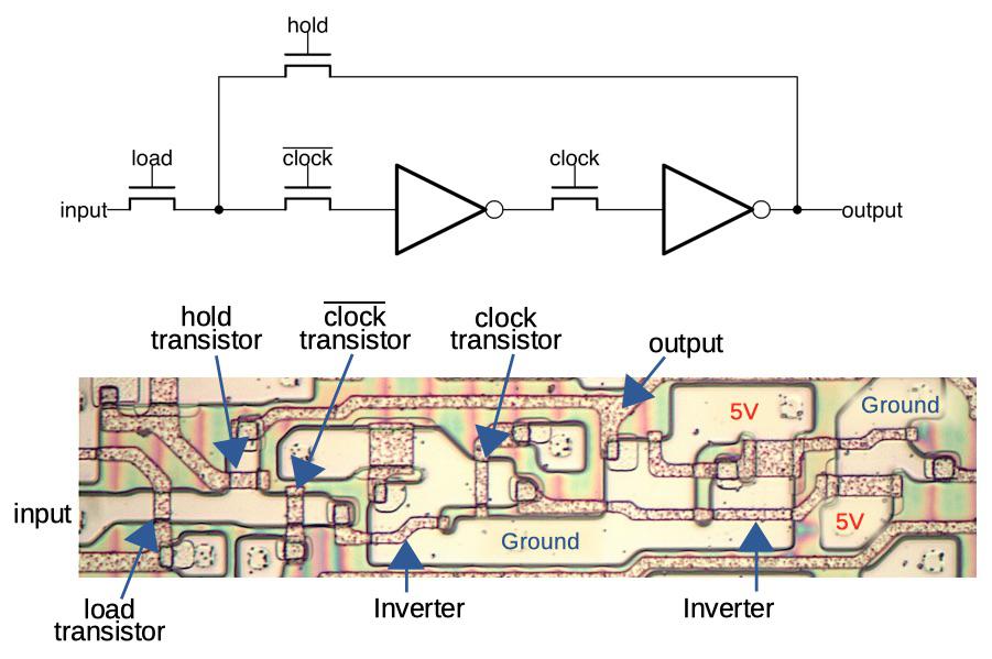
Microscopic photo of the latch in the 8086 processor. The metal layer with the conductors has been removed, but its traces are visible in the form of reddish vertical lines. Photo rotated 180 ° to fit the layout.
The latch uses output buffers not marked in the diagram to provide high current signals for the output and inverted output. These buffers have a funny name, "superbuffers" - because they deliver much higher current than a typical N-MOS inverter. The problem with an N-MOS inverter is that it runs slowly when driving some high capacity circuit. Since the superbuffer delivers more current, it switches the signal much faster. It achieves this by replacing the pull-up resistor with a transistor that delivers more current. The downside is that the pull-up transistor requires an inverter to operate, so the superbuffer circuit is more complicated. Therefore, the superbuffer is used only when needed - usually when sending a signal to many gates or when driving a long bus.
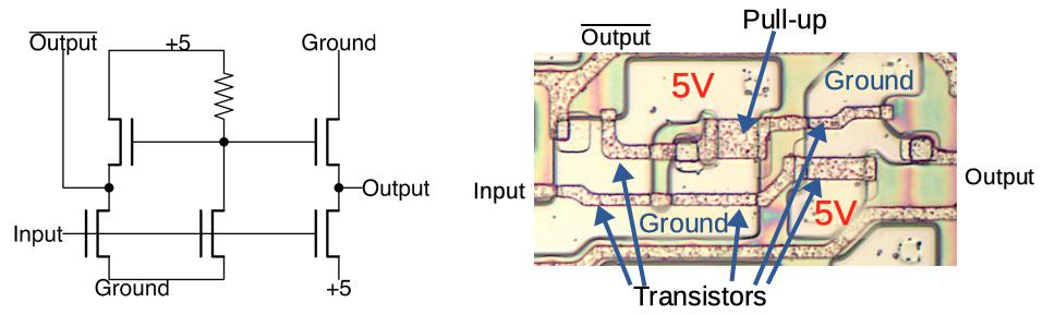
The 8086 latch implementation of the superbuffer. Note that the +5 V and ground connections are moved to the right-most transistors.
The diagram above shows a schematic of the 8086 latch superbuffer. Unlike a conventional superbuffer, this has both an inverting and a non-inverting superbuffer. To understand the circuit, note that the center resistor and transistor form an inverter. The inverter output is connected to the upper transistors, and the non-inverted input is connected to the lower transistors. Then, if the input is 1, the lower transistors turn on, and if the input is 0, then thanks to the inverter, the upper transistors turn on. Then, if the input is 1, the lower transistors will pull the output up, and the corresponding output - down. If the input is 0, then the upper transistors will pull the output down, and the corresponding output- up.
The problem with the N-MOS inverter is that the pull-up resistor has a limited current. When the output is 0, the transistor in the inverter quickly and with relatively high current pulls the output down. However, if the output is 1, the output is pulled up by a much weaker pull-up resistor.
A superbuffer is similar to a CMOS inverter in that it has a pull-up transistor and a pull-down transistor. The difference is that CMOS uses P-MOS and N-MOS transistors, while P-MOS uses an inverted gate input. Conversely, an N-MOS superbuffer requires a separate inverter. In other words, a CMOS inverter uses two transistors, and a superbuffer is much less efficient because it requires four transistors.
The superbuffer uses an enhancement mode transistor for pulling up and an enhancement mode transistor for pulling down. The threshold voltage of a transistor with its own channel is below zero, which allows its output to be pulled up to 5 V, and not to be turned off at a lower voltage. When the output is low, the self-channeling transistor will still be on, and will act like a normal pull-up in a conventional inverter, so a certain current will flow through it. You can read more about the superbuffer here .
Command register
Like most processors, the 8086 has an instruction register where the currently executing instruction is stored. In the 8086, the command register holds the first byte of the command (which can be multiple bytes), so it is made up of eight latches. One would think that they would be identical, however, each of them has its own shape. The layout of the 8086 is highly optimized, so the shape of each latch is designed to make the best use of the available space due to the limitations of the surrounding conductors. In particular, note that some latches connect together and share power and ground. Apparently, for the same reason, the latches do not go in a row.
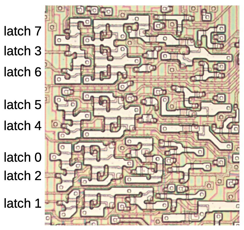
All 8 latches have slightly different shapes, optimized for the surrounding conductors. Earlier in the article, latch # 1 was rotated 180 °. Red vertical lines are traces of the removed metal layer.
The team travels the 8086 in a winding path. The processor uses performance-enhancing prefetching, loading instructions from memory before they are needed. They are stored in the command queue, a 6-byte queue located in the middle of a set of registers. By comparison, modern processors have a command cache that can be as large as several megabytes.
When a command is executed, it is stored in the command register, approximately in the center of the chip. The relatively large distances explain the need for a superbuffer. The command register feeds the command to the "group decryption ROM". This ROM defines the high-level characteristics of the command - whether it is single-byte, or multibyte, or it is the command prefix. And this is only a small part of the complex 8086 instruction processing system. Other latches hold parts of the instructions, marking register usage and ALU operations, and a separate circuit controls the microcode engine - but I will describe this separately.
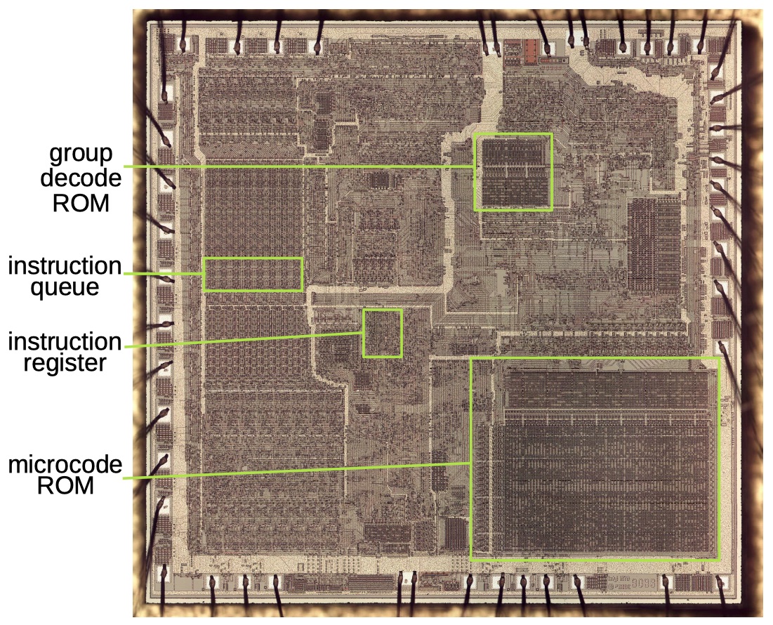
Crystal 8086, key components for command processing are marked. Along the perimeter, soldering wires connect the crystal to external contacts.
Conclusion
The 8086 makes extensive use of dynamic latches to store internal states. They are visible under a microscope and their circuits can be traced and understood. The 8086 crystal is interesting to analyze because, unlike modern processors, its transistors are large enough to be seen under a microscope. It was a sophisticated processor with 29,000 transistors for its day, yet simple enough for its circuits to be traced and understood.