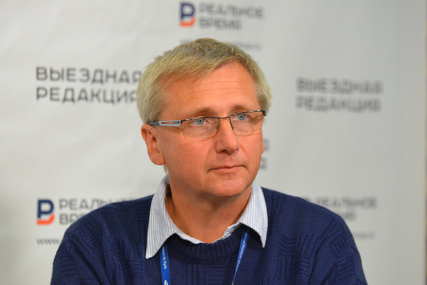
Inside - briefly about the essence of the opening with comments from the head of SAIT Russia, Ph.D. Stanislav Polonsky.

2D materials are key to overcoming scalability issues
SAIT is dedicated to the research and development of two-dimensional (2D) materials - crystalline substances made up of a single layer of atoms. In particular, the institute's specialists worked on the study and development of graphene and achieved revolutionary results in this area - they created a new graphene transistor, as well as a new method for the production of large-area single-crystal plates from flake graphene. In addition, SAIT scientists are busy accelerating the commercialization of the material.
“To improve the compatibility of graphene with silicon-based semiconductor processes, growing graphene films on semiconductor substrates must be carried out at temperatures below 400 ° C,” said Hyun Jin Shin, project manager for graphene development and principal investigator at SAIT. "We are also constantly working to expand the scope of graphene, not limited to semiconductors."
Transformed 2D material - amorphous boron nitride
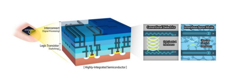
A recently discovered material called amorphous boron nitride (a-BN) is composed of boron and nitrogen atoms with an amorphous molecular structure. Despite the fact that amorphous boron nitride is obtained from white graphene, which includes boron and nitrogen atoms located in a hexagonal structure, due to its molecular structure, the new material has unique differences from white graphene.
Amorphous boron nitride has a best-in-class ultra-low dielectric constant of 1.78 with strong electrical and mechanical properties and can be used as an interconnect insulation material to reduce electrical interference. It has also been demonstrated that scaly material can be grown at low temperatures, as low as 400 ° C. As such, amorphous boron nitride is expected to be widely used in semiconductors such as DRAM and NAND solutions, and especially in next generation memory for large-scale servers.
 Stanislav Polonsky, Head of Advanced Research and Development, Samsung Research Center:
“The speed of modern semiconductor integrated circuits is determined not only by the switching speed of transistors, but also by the speed of propagation of electrical signals from one transistor to another. From the point of view of a signal-sending transistor, a signal-transmitting wire is a capacitor that needs to be charged. The smaller the capacity of such a capacitor, the faster it charges, the faster the signal is transmitted. The capacitance of a capacitor decreases with the dielectric constant of the insulator surrounding the metal wire. The record low values of this parameter obtained by Korean scientists will lead to record high signal transmission rates on the microcircuit, increasing its performance. It's simple! "
Briefly about the achievements of SAIT in recent years:
2012: Graphene Barristor, Triode Device with Gate Operated Schottky Barrier (SAIT, Published in Science)
2014: Flake Growth of a Monocrystalline Graphene Monolayer Plate on Reusable Hydrogen-Terminated Germanium (SAIT and Songyungwan University, Published in Science)
2017: Realization of a Continuous Carbon Monolayer Zachariasen (SAIT and Sunggyungwan University, published in Science Advances)
2020: Ultra-low dielectric constant of amorphous boron nitride (SAIT, UNIST and University of Cambridge, published in Nature) News
source .