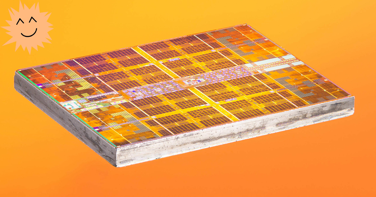
All the central processing units of any computer, be it a cheap laptop or a server for millions of dollars, have a device called a cache. And with a very high probability it has several levels.
It's probably important, otherwise why install it? But what does the cache do, and why does it have different levels? And what does "12-way set associative" mean?
What is cache?
TL; DR: This is a small but very fast memory located in close proximity to the logical blocks of the CPU.
However, we can of course learn much more about the cache ...
Let's start with an imaginary magic storage system: it is infinitely fast, can handle an infinite number of data transfers at the same time, and always provides reliable and secure storage. Of course, nothing of the kind exists anywhere near, but if this were so, the structure of the processor would be much simpler.
Processors would then only need logical blocks for addition, multiplication, etc., as well as a data transmission control system, because our theoretical storage system is capable of instantly transmitting and receiving all the necessary numbers; no logic block has to stand idle while waiting for data to be transferred.
But as we know, there is no such magic storage technology. Instead, we have hard drives or solid state drives, and even the best of them fall far short of the processing capabilities required of a modern processor.
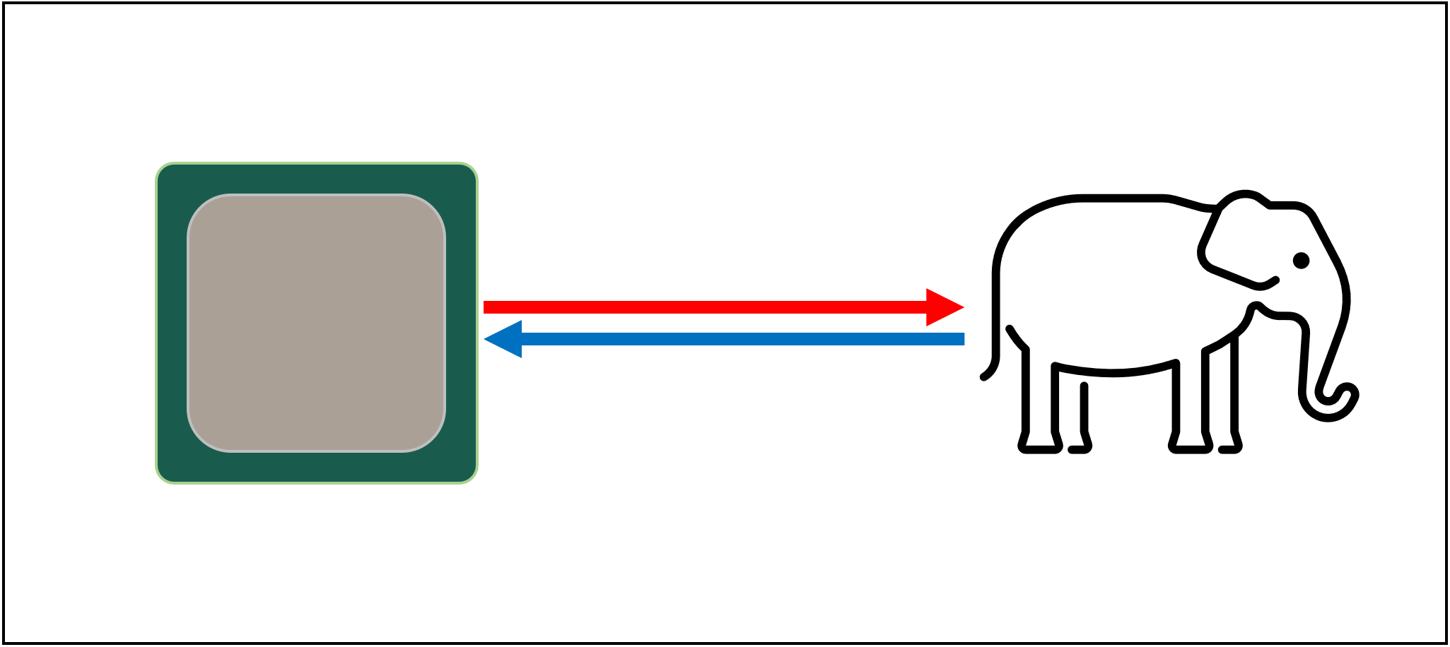
The Great T'Fon of Storage
The reason for this is that modern processors are incredibly fast - they only need one clock cycle to add two 64-bit integers; if the processor is running at 4 GHz, this is only 0.00000000025 seconds, or a quarter of a nanosecond.
At the same time, a spinning hard disk takes thousands of nanoseconds just to find data on the disks, let alone transfer it, and solid-state drives take tens or hundreds of nanoseconds.
Obviously, such drives cannot be built insideprocessors, so there will be a physical separation between them. Therefore, time is added to move data, which aggravates the situation.
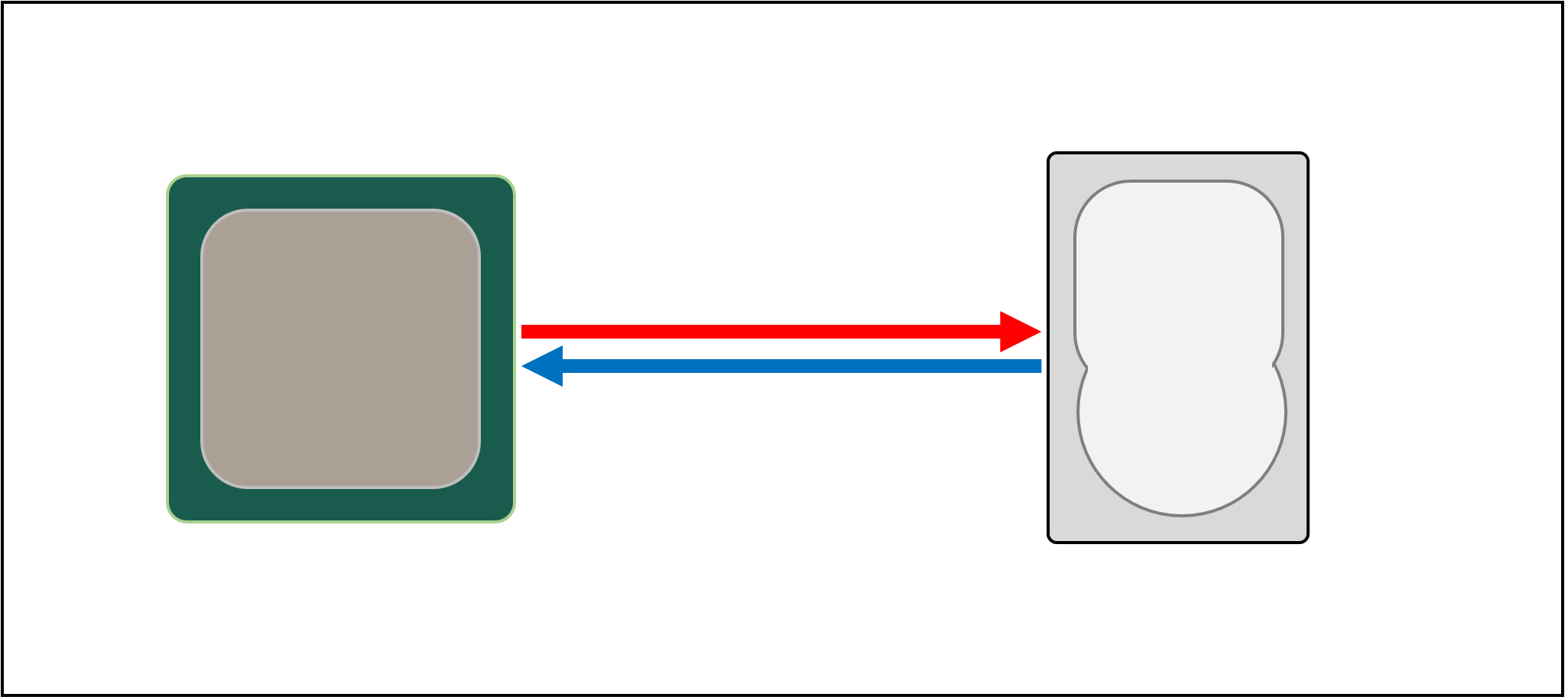
Alas, this is the Great A'Tuin of data storage
That is why we need another storage system located between the processor and the main drive. It should be faster than a storage device, capable of handling multiple data transfers simultaneously, and be much closer to the processor.
Well, we already have such a system, and it's called RAM ; it is present in every computer and performs exactly this task.
Almost all such storages are of the DRAM (dynamic random access memory) type ; they are capable of transferring data much faster than any storage device.

However, despite its enormous speed, DRAM is not capable of storing such amounts of data.
Some of the largest DDR4 memory chips developed by Micron store 32 Gb, or 4 GB of data; the largest hard drives store 4,000 times more.
So, although we have increased the speed of our data network, we will need additional systems (hardware and software) to figure out what data should be stored in a limited amount of DRAM, ready for processing by the processor.
DRAM can be manufactured in a chip package (this is called embedded DRAM). However, processors are quite small, so they cannot fit a lot of memory.
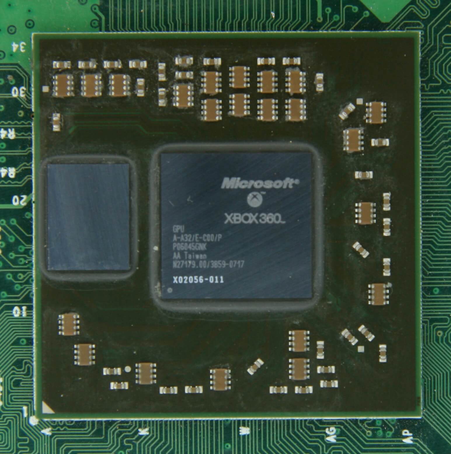
10MB DRAM to the left of the Xbox 360 GPU. Source: CPU Grave Yard
The vast majority of DRAM is located in the immediate vicinity of the processor, connected to the motherboard, and is always the component closest to the processor. However, this memory is still not fast enough ...
DRAM takes about 100 nanoseconds to find data, but at least it is capable of transferring billions of bits per second. It looks like we need another memory stage that can be placed between the CPU and DRAM blocks.
The remaining stage appears on the scene: SRAM ( static random access memory). DRAM uses microscopic capacitors to store data in the form of an electrical charge, while SRAM uses transistors for the same task, which operate at the same speed as the logical blocks of the processor (about 10 times faster than DRAM).

Of course, SRAM has a drawback, and again it has to do with space.
Transistor memory takes up much more space than DRAM: in the same size as a 4GB DDR4 chip, you can get less than 100MB of SRAM. But since it is manufactured using the same manufacturing process as the CPU, SRAM can be embedded directly inside the processor, as close as possible to the logical blocks.
With each additional step, we increased the speed of the transferred data at the cost of the stored volume. We can go on and add new steps, which will be faster, but smaller.
And so we got to a stricter definitioncache concepts: a collection of SRAMs located inside the processor; they maximize processor utilization by transferring and storing data at very high speeds. Are you satisfied with this definition? Great, because things will get much more complicated from now on!
Cash: multilevel parking
As we said above, the cache is necessary because we do not have a magic storage system that can handle the data consumption of logical blocks of the processor. Modern CPUs and GPUs contain many SRAMs, arranged in a hierarchy within - a sequence of caches with the following structure:

In the above image, the processor (CPU) is denoted by a dashed rectangle. On the left are ALUs (arithmetic logic units); these are structures that perform mathematical operations. Although not strictly a cache, the closest memory level to the ALU is registers (they are ordered in a register file ).
Each of them stores one number, for example, a 64-bit integer; the value itself can be an element of some data, a code of a specific instruction, or a memory address of some other data.
The register file in desktop processors is quite small, for example, in each of the Intel Core i9-9900K coresthere are two banks of such files, and the one for integers contains only 180 64-bit integers. Another register file for vectors (small arrays of numbers) contains 168 256-bit elements. That is, the total register file for each core is slightly less than 7 KB. For comparison, the Nvidia GeForce RTX 2080 Ti register file for streaming multiprocessors (as GPUs call CPU core analogs) is 256 KB in size.
Registers, like cache, are SRAMs, but their speed does not exceed the speed of the ALUs they serve; they transfer data in one clock cycle. But they are not designed to store large amounts of data (only one element), so there are always larger blocks of memory next to them: this is the first level cache (Level 1).
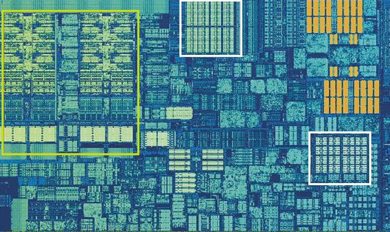
One Intel Skylake processor core. Source: Wikichip
The above image is an enlarged view of one of the cores of the Intel Skylake desktop processor .
ALU and register files are located on the left and are surrounded by a green frame. At the top of the photo, the Level 1 Data cache is indicated in white. It does not contain much information, only 32 KB, but like registers, it is located very close to logical blocks and operates at the same speed with them.
Another white rectangle on the right shows the Level 1 Instruction cache, also 32 KB in size. As the name implies, it stores various commands ready to be split into smaller micro-ops.(usually denoted by μops) that ALUs must execute. There is also a cache for them, which can be classified as Level 0, because it is smaller (contains only 1,500 operations) and closer than L1 caches.
You may be wondering why are these SRAMs so small? Why aren't they megabytes in size? Together, the data and instruction caches occupy almost the same area on the chip as the main logic blocks, so their increase will lead to an increase in the total die area.
But the main reason for their size of several kilobytes is that as the memory capacity increases, the time required to search and retrieve data increases. L1 cache needs to be very fast, so there is a tradeoff between size and speed - at best, it takes about 5 clock cycles to get data from this cache (more for floating point values).
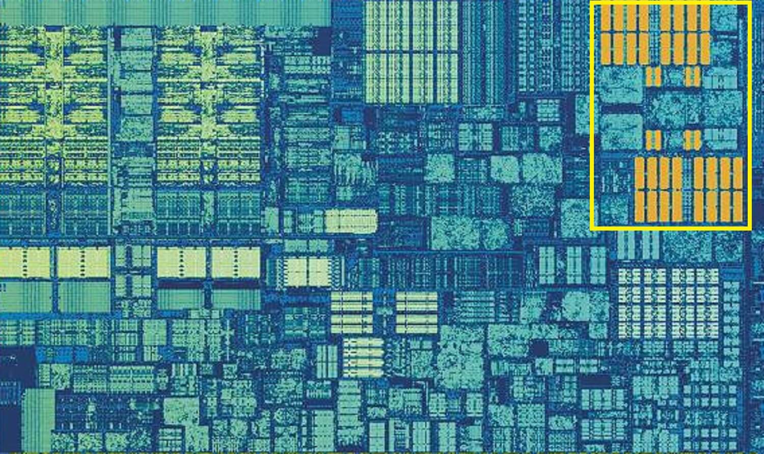
Skylake's L2 cache: 256KB SRAM
But if this were the only cache inside the processor, its performance would run into an unexpected hurdle. That is why another layer of memory is built into the kernels: the Level 2 cache. This is a generalized storage block containing instructions and data.
It is always larger than Level 1: in AMD Zen 2 processors, it takes up to 512KB to provide enough data for the lower-level caches. However, the large size requires sacrifice - it takes about twice as long to find and transfer data from this cache compared to Level 1.
In the days of the first Intel Pentium, the Level 2 cache was a separate chip, either installed on a separate small board (like DIMM RAM), or built into the main motherboard. Gradually, it moved into the case of the processor itself, and finally, it was fully integrated into the chip crystal; this happened in the era of processors such as the Pentium III and AMD K6-III.
This achievement was soon followed by another level of cache needed to support lower levels, and it arrived just in time for the heyday of multi-core chips.
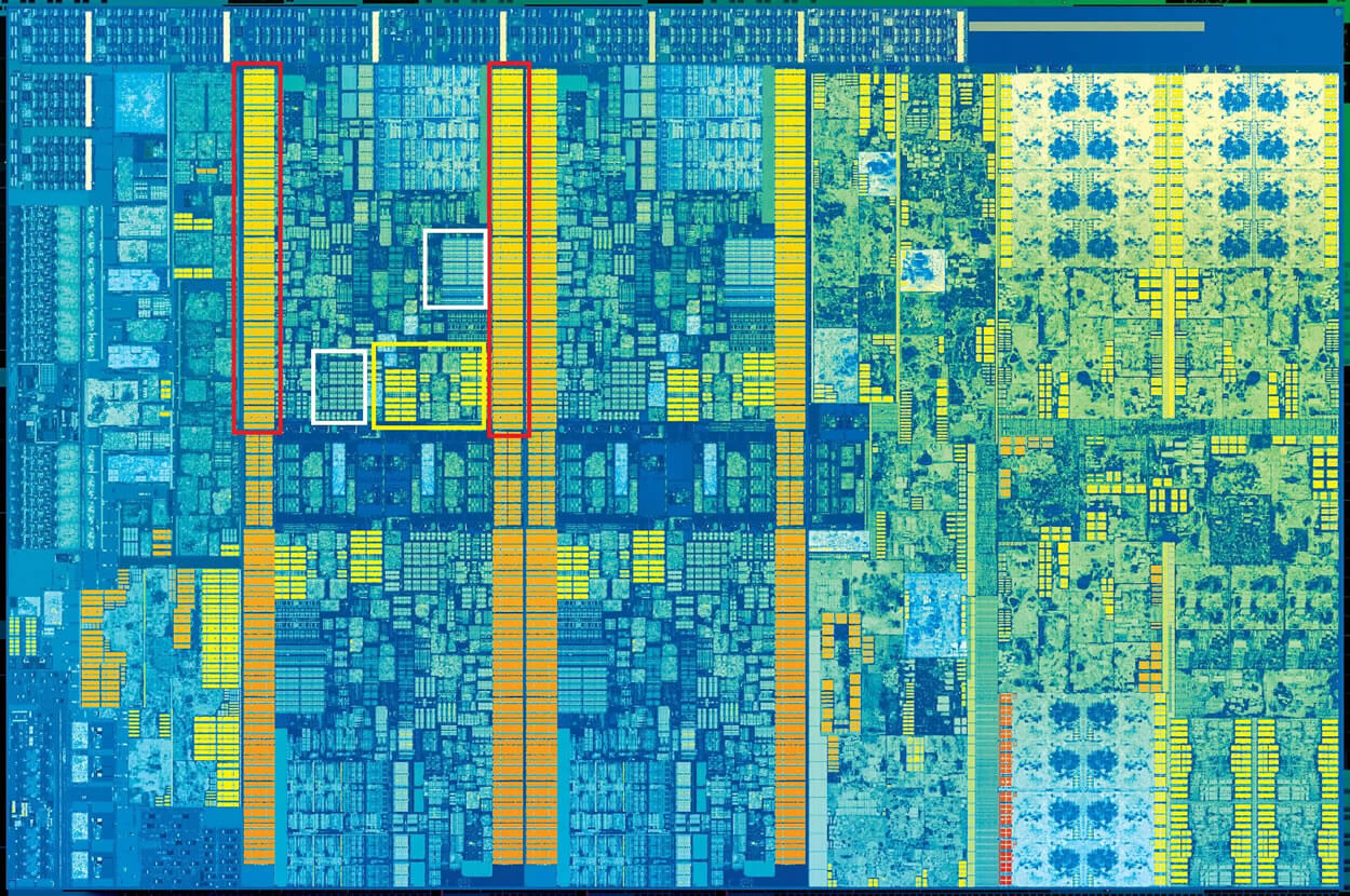
Intel Kaby Lake chip. Source: Wikichip
This image of the Intel Kaby Lake chip shows four cores on the left (the integrated GPU takes up almost half the die and is on the right). Each core has its own "personal" set of Level 1 and 2 caches (highlighted in white and yellow boxes), but they also have a third set of SRAM blocks.
The third level cache (Level 3), although located directly next to one core, is completely common to all the others - each core can freely access the contents of the L3 cache of another core. It is much larger (2 to 32 MB), but also much slower, averaging over 30 cycles, especially when the kernel needs to use data residing in a cache block far away.
Shown below is one core of AMD Zen 2 architecture: 32KB Level 1 data and instruction caches (in white boxes), 512KB Level 2 cache (in yellow boxes), and a huge 4MB L3 cache block (in red box).

Zoomed in on a single core of an AMD Zen 2 processor. Source: Fritzchens Fritz
But wait: how can 32KB take up more physical space than 512KB? If Level 1 stores so little data, why is it disproportionately large compared to L2 and L3 caches?
Not just numbers
The cache improves performance by speeding up the transfer of data to logical blocks and keeping a copy of frequently used instructions and data nearby. The information stored in the cache is divided into two parts: the data itself and the place where it is originally located in the system memory / storage - this address is called the cache tag .
When the processor performs an operation that needs to read or write data from / to memory, it starts by checking the tags in the Level 1 cache. If the required data is there (a cache hit has occurred ), then this data is almost At once. A cache miss occurs when the required tag is not found at the lowest level in the cache.
A new tag is created in the L1 cache, and the rest of the processor architecture takes over, looking in other levels of the cache (up to the main storage, if necessary) for the data for that tag. But to free up space in the L1 cache for this new tag, something must be thrown into L2.
This results in near-constant shuffling of data, performed in just a few clock cycles. The only way to achieve this is by creating a complex structure around SRAM to handle data management. In other words, if the processor core consisted of only one ALU, then the L1 cache would be much simpler, but since there are dozens of them (and many of them juggle with two instruction streams), the cache requires many connections to move data.
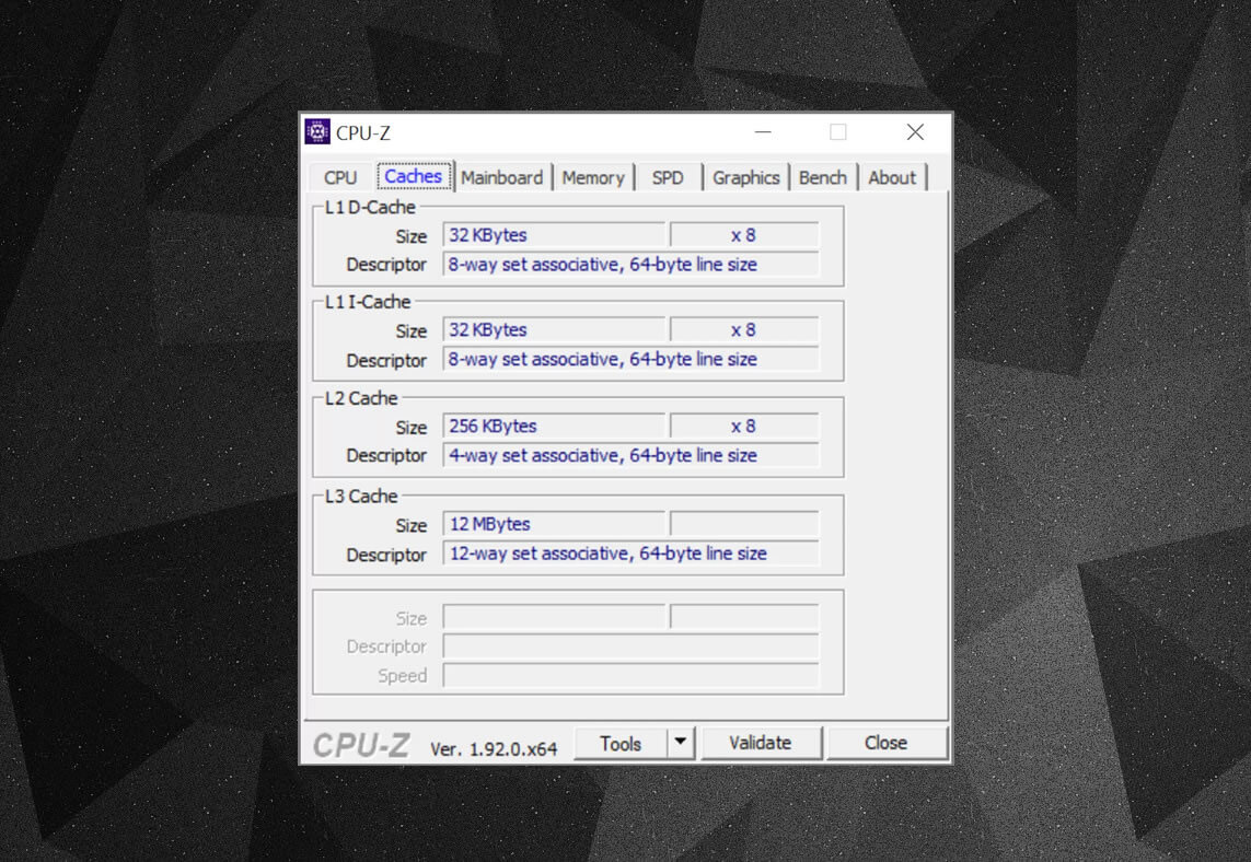
You can use free software such as CPU-Z to examine the cache information in your computer's processor . But what does all this information mean? An important element is the set associative label , which indicates the rules used to copy blocks of data from system memory to the cache.
The above cache information is for Intel Core i7-9700K . Each of its Level 1 caches is divided into 64 small blocks, called sets , and each of these blocks is also broken into cache lines.(64 bytes in size). "Set associative" means that a block of data from the system is bound to cache lines in one particular set, and cannot be freely bound to some other place.
"8-way" means that one block can be associated with 8 cache lines in the set. The higher the level of associativity (that is, the larger the “way”), the more chances of a cache hit during a processor lookup and the less loss caused by cache misses. The disadvantages of such a system are the increased complexity and power consumption, as well as lower performance, because more cache lines must be processed for each block of data.
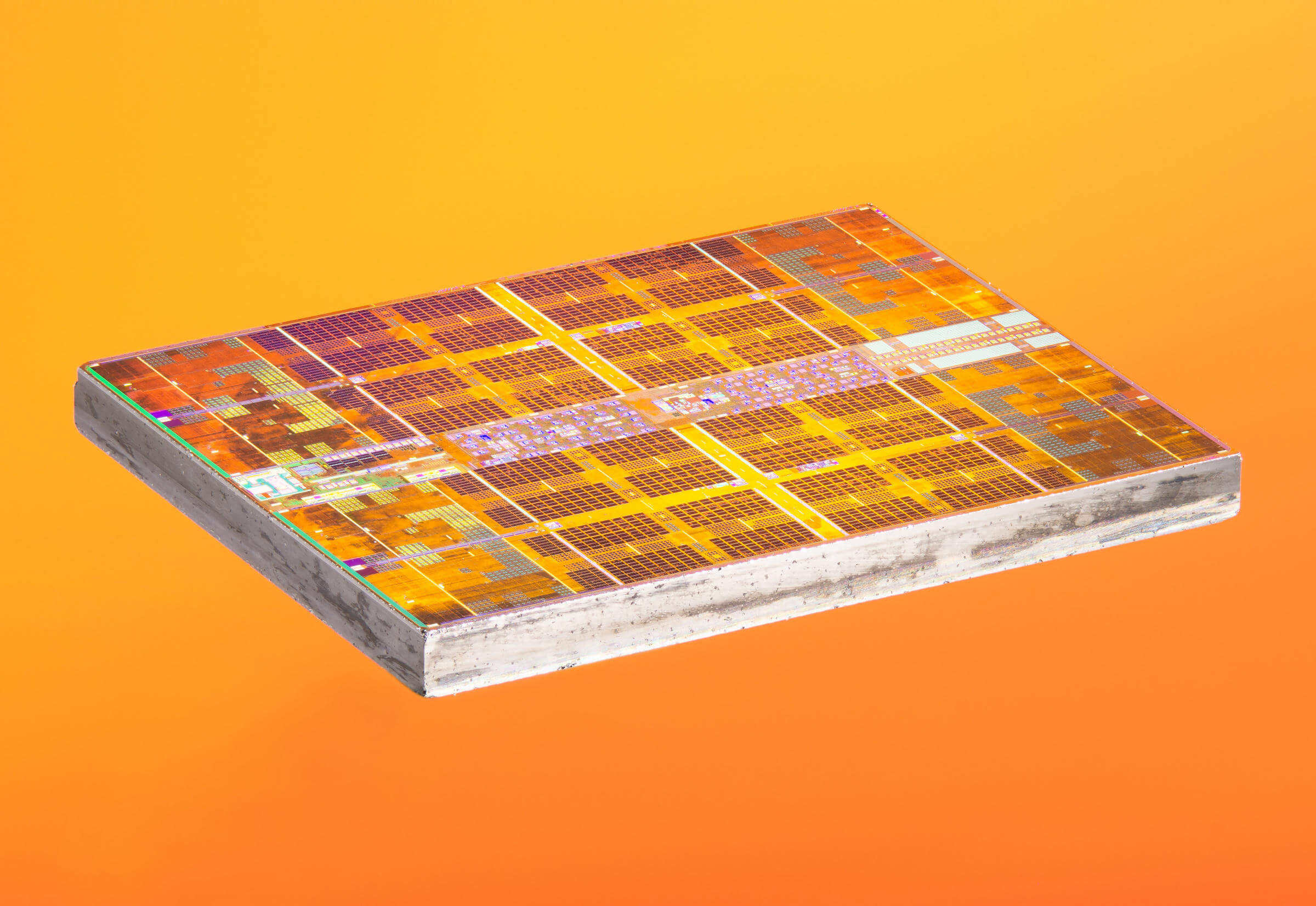
Inclusive cache L1 + L2, victim cache L3, write-back policies, there is even ECC. Source: Fritzchens Fritz
Another aspect of cache complexity has to do with how data is stored between different tiers. The rules are set in the inclusion policy . For example, Intel Core processors have fully inclusive L1 + L3 caches. This means that some data in Level 1, for example, may be present in Level 3. It may seem like a waste of valuable cache space, but the advantage is that if the processor misses the tag in the lower level, it does not need search the top level for data.
In the same processors, the L2 cache is non-inclusive: all data stored there is not copied to any other layer. This saves space, but causes the chip's memory system to look for a missing tag in L3 (which is always much larger). Victim caches have a similar principle, but they are used to store information carried from lower levels. For example, AMD Zen 2 processors use the victim cache L3, which simply stores data from L2.
There are other cache policies, such as writing data to both the cache and main system memory. These are called write policies ; most modern processors use write-back caches- this means that when data is written to the cache layer, there is a delay before writing a copy of it to system memory. Most often, this pause lasts as long as the data remains in the cache - RAM receives this information only when it is "popped" from the cache.
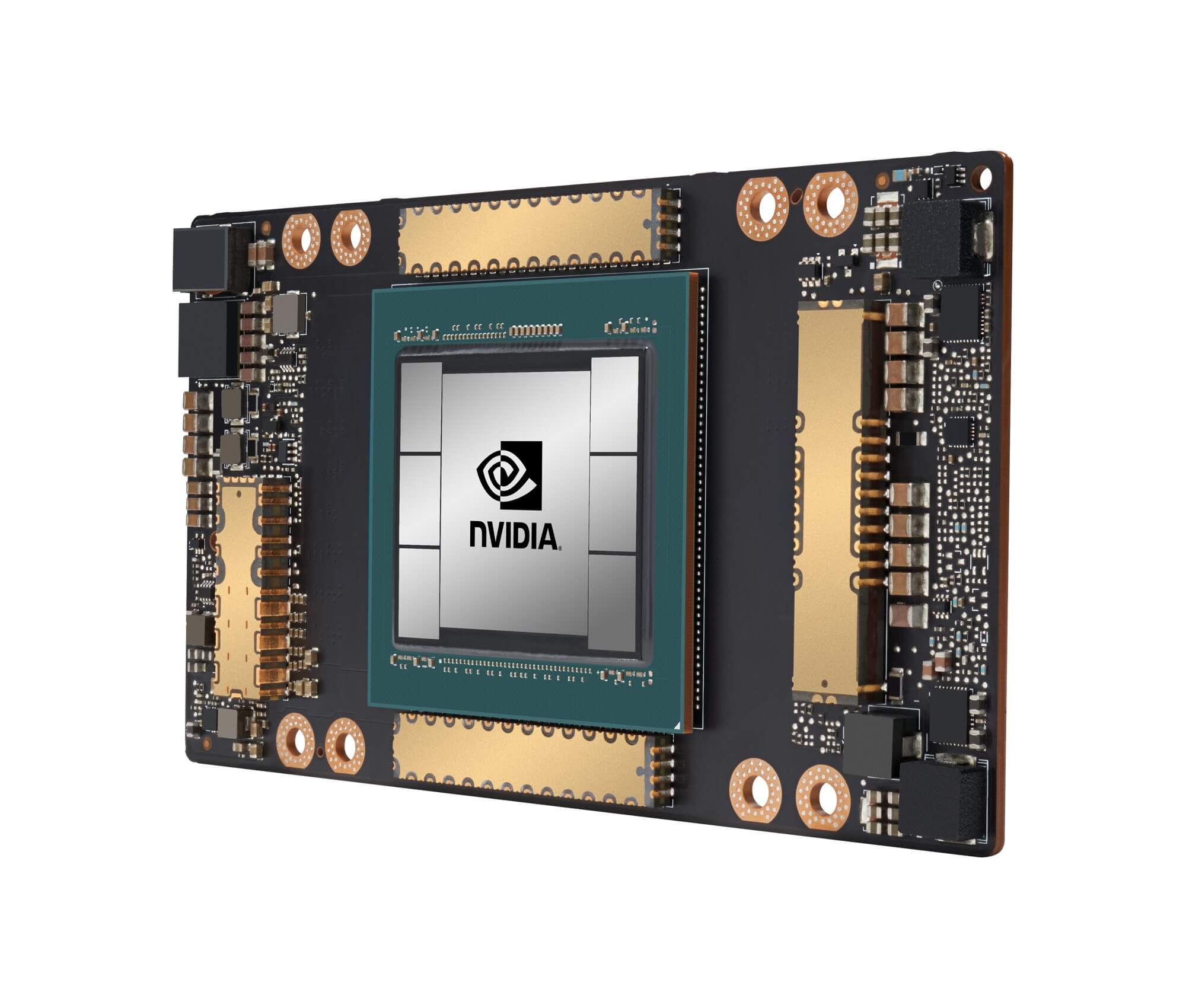
Nvidia GA100 GPU with 20 MB L1 cache and 40 MB L2 cache
For processor designers, the choice of cache size, type, and policy is a matter of balancing the drive to increase processor power with increasing complexity and chip footprint. If it were possible to create 1000-channel 20MB Level 1 associative caches such that they did not occupy the area of Manhattan (and did not consume the same amount of power), then we would all have computers with such chips!
The lowest level of caches in modern processors has remained virtually unchanged over the past decade. However, the Level 3 cache continues to grow in size. If you had $ 999 for an Intel i7-980X ten years ago, you could have a 12MB cache. Today for half that amountavailable for purchase 64 MB .
To summarize, the cache is an absolutely essential and awesome device. We have not covered other types of caches in the CPU and GPU (for example, associative translation buffers or texture caches), but since they all have the same simple structure and layout of levels, it will not be difficult to understand them.
Have you had a computer with L2 cache on the motherboard? How about slotted Pentium II and Celeron (eg 300a ) daughterboards? Remember your first shared L3 processor?
Advertising
Our company offers for rent servers with processors from Intel and AMD. In the latter case, these are epic servers! VDS with AMD EPYC , CPU core frequency up to 3.4 GHz. The maximum configuration is 128 CPU cores, 512 GB RAM, 4000 GB NVMe.
