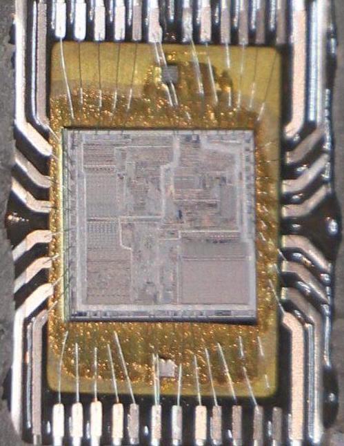
Enlarged photo of the 8086 chip; silicon die and wire-wiring visible The
revolutionary Intel 8086 microprocessor, introduced in 1978, spawned a whole family of x86 processors that are still used in desktop and server computers today. The chip is built on digital circuits, but it also contains analog circuits: charge pump generators that turn the processor's 5 V power supply into a negative voltage to increase performance. I am reverse-engineering an 8086 based on a photo of the crystal, and in this post I describe the design of these charge pump generators and how they work.
Strictly speaking, of course, the entire chip is made of analog components. As the old saying goes, "digital computers are made from analog components." Its author is DEC engineer Don Vonada, and his aphorisms were published in Computer Engineering magazine in 1978.
Vonada's Engineering Aphorisms
- There is no “land”.
- Digital computers are made from analog components.
- Circuit prototypes always work.
- First, approved temporary conditions are developed, and then unapproved ones are found.
- If all but one switch in a conductor group, then it also switches.
- If all but one switch in the gate group is switched, then it also switches.
- Each picofarad has its own nanogenry.
- Capacitors convert voltage faults into current faults (energy conservation law).
- – , , .
- .
- – , .
- .
- , .
- 95% . 5% — .

Photo of the crystal of the 8086 microprocessor. On the left are the ALU and registers. Bottom right - ROM with microcode. The link with the photo opens a larger photo. Follow this link - the original photo (10,000 × 10,000 px, 24 MB - does not fit on habrastorage).
The photo above shows a tiny 8086 chip under a microscope. A metal layer is visible on top of the chip, under which silicon is hidden. Along the outer edge, you can see the soldering wires connecting the contact pads of the crystal with 40 external contacts of the chip. But if you look closely, you can see that the crystal has 42 sites. Why does he need two extra?
An integrated circuit is built on a silicon substrate on which transistors are applied. For high-speed ICs, it is useful to apply a negative " bias voltage to the substrate.For this, many chips from the 1970s have an external contact, which is supplied with 5 V, but it was inconvenient for engineers to use an additional power supply. negative voltage in place. These chips use the convenient single +
5V supply , and all engineers are happy. There are several advantages to supplying negative bias voltage. It reduces parasitic capacitance, which makes the chip faster, makes the threshold voltage of transistors more predictable, and reduces current leakage.
Early DRAM and microprocessor chips often required three supply voltages: +5 V (Vcc), +12 V (Vdd), and -5 V (Vbb). In the late 1970s, improvements in chip technology made it possible to use a single voltage. For example, the MK4116 (16K bit DRAM from Mostek from 1977) required three voltages, and the improved MK4516 (1981) operated with a single + 5V, which simplified circuit design. It's funny that some of the newer chips had Vbb and Vcc pins not connected to anything for backward compatibility.
Intel's memory chips took a similar path: DRAM 2116 (16 KB, 1977) used three voltages, while the improved 2118 (1979) used just one. Similarly, the famous Intel 8080 microprocessor (1974) used induced channel MOSFETs and required three voltages to operate. The Microprocessor Motorola 6800 (1974) took a different approach, operating with a single supply voltage; although the 6800 was built with an old-style transistor, it did not need + 12V external power as it implemented a voltage doubler in place.
The two extra pads on the 8086 chip are needed to apply bias voltage to the substrate. The photo at the beginning of the article shows the location of the silicon crystal on the chip, with jumper wires connecting it to the contact pad that forms the external contacts. The photo shows two small gray squares above and below. Each of them is connected to one of the "extra" sites. The charge pump on the 8086 chip generates a negative voltage passing through the desoldering wires to these squares, and then through the metal plate under the 8086 substrate.
How charge pump generators work
In the photo below, two generators for pumping the charge of the 8086 processor are highlighted. the lower one works the same way, it is simply arranged differently to fit into the available space. Each generator has a driver circuit, a large capacitor and a pad with a wire connecting it to the substrate. Each generator is located adjacent to one of the 8086's two ground pads, probably to minimize electrical noise.

Photo of an 8086 chip with oversized bias voltage generators
You may be wondering how the charge pump turns a positive voltage into a negative voltage. The trick in using a "flying" capacitor, the diagram of which is below. On the left, the capacitor is charged to 5 V. Disconnect it and connect the positive side to ground. The capacitor still has a 5V charge, so the bottom of the capacitor should deliver -5V. By quickly switching the capacitor between the two states, the charge pump generates negative voltage.

The 8086 charge pump uses a MOSFET and diodes to switch the capacitor between states, and a generator to drive the transistor - as shown in the diagram below. The ring generator consists of three inverters connected in a loop (ring). Since the number of inverters is odd, the system is unstable and fluctuates. If it had an even number of inverters, it would be stable in one of two states. This technique is used in registers 8086 - a pair of inverters store a bit.
For example, if the first inverter receives 0, it will output 1, the second output will be 0, and the third output 1. This switches the first inverter, and this switching moves in a loop, resulting in oscillations. To slow down the speed of the oscillation, two RC circuits are inserted into the ring... Since it takes some time to charge and discharge the capacitor, the oscillation slows down, giving the charge pump time to operate.
I tried to measure the frequency of the charge pump by studying the chip current in search of oscillations. I measured fluctuations at 90 MHz, but I suspect I could actually measure noise.

Circuit of a charge pump generator in the Intel 8086, giving negative bias voltage on the substrate
The outputs from the capacitor come to the transistor capacitor driver. The first step turns on the top transistor, which forces the capacitor to charge through the first diode to 5V with respect to ground. In the second step, all the magic happens. The bottom transistor turns on, and connects the top of the capacitor to ground. Since the capacitor is still charged to 5V, the bottom should be delivering -5V, which gives us the negative voltage we want. The current flows through the second diode and the soldering wire to the substrate. When the oscillator switches again, the upper transistor turns on and the cycle repeats. The charge pump is so called because it pumps the charge from the outlet to the ground. Diodes are similar to water pump isolation valves in that they move the charge in the right direction.
Of course, I have simplified the scheme of work a little. Due to the voltage drop across the transistor, the substrate voltage will be -3 V, not -5 V. If the chip needs a higher voltage drop, you can make a cascade of several charge pump generators. When I talk about the direction of the generator, I mean the direction of the current. If you imagine pumping electrons, then assume that negatively charged electrons are pumped in the opposite direction into the substrate.
Implementation in silicon
The photo below shows the implementation of the charge pump generator on the chip. The photo above shows the metal conductors, under which there is a reddish polysilicon. Below is beige silicon. In the center is the main capacitor, with H-shaped conductors connecting it to the circuit on the left. Part of the capacitor is hidden under the wide metal power path at the top. On the right, the jumper wire is connected to the pad. There is a test pattern under the pad - a square for each mask used to apply the next layer to the chip.

Metal layer charge pump
After removing the metal layer, the diagram becomes more visible. The right half of the photo is occupied by a large charge pump capacitor. It is, of course, microscopic, but huge by chip standards - roughly comparable to a 16-bit register. The capacitor consists of polysilicon above the silicon, between which an insulating oxide is interposed. Polysilicon and silicon form the capacitor plates. On the left are a smaller capacitor and resistors that give the generator an RC delay. Below them is the generator circuit and transistors.
The generator is assembled from 13 transistors. Seven transistors form 3 inverters (one transistor has an additional inverter for additional output current). Of the six driver transistors, two pull the output up and four down. The circuit is oddly different from a normal inverter circuit because the current requirements are different from normal digital logic.

Key components of the 8086 Charge Pump. The metal layer has been removed and the polysilicon and silicon layers are visible.
One interesting feature of the charge pump is that there are two diodes, each with eight transistors spaced at regular intervals. The diagram below shows the structure of the transistor. A transistor can be thought of as a switch that allows current to flow between its two sections, the source and drain. The transistor is controlled by a gate made of a special type of silicon, polysilicon. A high gate voltage allows current to flow between source and drain, while a low gate blocks current. These tiny transistors can be combined to form logic gates — components of microprocessors and other digital chips. However, in this case, transistors are used as diodes.

The structure of transistors implemented in IC
The photo below shows a top view of the transistor in the charge pump generator. As in the diagram, polysilicon forms a gate between the silicon doped regions on both sides. A diode can be made from a MOS structure by connecting the gate and drain through the silicon / polysilicon junction located at the bottom of the photo. Silicon can also be bonded to the metal layer through through contacts. For this photo, the metal layer has been removed, but the remaining faint circles indicate the location of the through contacts.

A transistor in the charge pump generator circuit. A polysilicon gate separates the source and drain of the transistor.
The diagram below shows how two diodes are assembled from 16 transistors. To support a relatively large current of the charge pump generator, 8 parallel transistors are used in each diode. Note that the neighboring transistors have a common source and drain, which is why they were packed so tightly. Blue lines mark where the metal wires were - they were removed for this photo. The dark circles are the places where there were through contacts between the metal and silicon.

The charge pump has two diodes, each made of 8 transistors. The source, gate and drain are identified by the letters S, G and D.
As a result, the origins of the top eight transistors are connected to ground by a metal wire. Their gates and drains are connected by polysilicon under the transistors, as a result of which diodes are obtained from them. They are connected to the capacitor with a metal wire. The eight lower transistors form the second diode. Their gates and drains are connected by a lower metal loop. Note how the layout of the elements has been optimized; for example, the breeches are bent so as not to touch the through contacts.
Conclusion
The bias voltage generator on the 8086 chip is an interesting combination of a digital circuit (a ring generator made up of inverters) and an analog charge pump. It may seem like a long-forgotten device from the history of computers in the 1970s, but in fact it is present in modern ICs as well. In modern chips, this is a much more complex circuit, carefully tuned to provide several adjustable bias voltages in areas with separate power supplies. In some ways, it is similar to the x86 architecture, which began its way in the 1970s and has become even more popular today, but as part of the constant improvement in efficiency, its complexity has increased incredibly.
Bias generators are marketed today as off-the-shelf proprietary ideas- you can buy a circuit of such a generator and insert it into your chip project (see links 1 , 2 , 3 , 4 , 5 , 6 ). There is even an IEEE 1801 power standard that IC design tools can generate the required circuits.
The Intel 8087 math coprocessor attached to the 8086 also has its own bias voltage generator. It works on the same principles, however, oddly enough, it uses a different circuit with 5 inverters.