However, using or debugging a DAC / ADC can be difficult due to the limitations set by the hardware manufacturer, for example, on the software used or on how the device can be controlled. This suggests designing your own interaction model.
In this article we will consider the possibility of organizing interaction between a PC and a DAC / ADC using FPGAs.

Foreword
The main purpose of this article is to describe the solution to a specific problem, as well as familiarity with the interfaces of interaction of integrated circuits (IC). The main purpose of the DAC / ADC is not considered here.
This article requires some knowledge of object-oriented programming and circuitry, so if you are not familiar with these concepts, it is recommended to start with them.
I hope that the experience of a person who first encounters the problem of communication of electronic devices will be useful to someone.
Good luck and new achievements to everyone!
A small educational program on interfaces
Disclaimer
If you are familiar with the structure of the main interfaces used for IC communication, you can safely skip this point.
educational program
, .
, (, .) . , .
, . , , , .. , . . – , . , . , .
, .
( ), :
«-» — , . , — .

«» (, « » «») , . . , , , . .

( «») . , , , - . .
:
, . . . , .

, . , , .

(-/)
:
. .

, .
: , «» .
. .
:
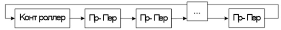
. . . ( – , – , , ). « » ( ). .

, , .

() SPI I2C UART.
I2C – . I2C . I2C «-», .
, , . , . 7- 16 . , 112 . I2C (SDA) (SCL).

I2C
SPI – , .
SPI «-». MOSI SCLK, . MISO, . SS.
SPI
UART – – , .
RxD ( ) TxD ( ).
UART TxD . . UART , , UART , . , . 8 ( ), , .
UART «-». , UART . « » «».

UART
, .
, (, .) . , .
, . , , , .. , . . – , . , . , .
, .
( ), :
- «-»;
- «»;
- «» («»).
«-» — , . , — .
«» (, « » «») , . . , , , . .
( «») . , , , - . .
:
- ;
- ;
- -.
, . . . , .
, . , , .
(-/)
:
- ();
- ();
- ().
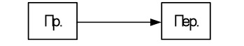
. .
, .
: , «» .
. .
:
- ;
- .
. . . ( – , – , , ). « » ( ). .
, , .
?
() SPI I2C UART.
I2C
I2C – . I2C . I2C «-», .
, , . , . 7- 16 . , 112 . I2C (SDA) (SCL).
I2C
SPI
SPI – , .
SPI «-». MOSI SCLK, . MISO, . SS.
SPI
UART
UART – – , .
RxD ( ) TxD ( ).
UART TxD . . UART , , UART , . , . 8 ( ), , .
UART «-». , UART . « » «».
UART
What is this DAC?

It seems not this
To begin with, let's define the DAC / ADC used: The
Analog Devices AD9993-EBZ debug board is a device that combines four 14-bit ADCs and two 14-bit DACs.
The operating modes of this IC are controlled by changing the state of its internal registers. The AD9993 uses 66 registers with a stored (processed) word size of 8 bits, the addresses of which are described by three-bit hexadecimal values (12 data bits). Two types of commands are supported - read command and write command. In other words, in order to correct the operation of the IC, it is necessary to send a command to write some valid 8-bit value to a specific register address. Access to the registers of this IC is carried out through the serial peripheral interface (SPI), the connection to which on the debug board is realized through the 40-pin FIFO_0 connector or through an additionally installed contact group.

Like this one (FIFO_0 - top gray connector)
Basic requirements for SPI limit parameters:
- Maximum data transmission frequency - 25 MHz;
- The duration of the upper and lower levels on the sync signal generation line is 10 ns;
- Level setting time on data transmission lines and on resolution lines - 2 ns;
- Level holding time on data transmission lines and on resolution line - 2 ns;
- The guaranteed time of validity of one data bit on the transmission line of the slave device is 2 ns.
A complete description of the device's features can be found in its documentation .
What does the manufacturer say?
Recommended control scheme
Based on the AD9993-EBZ documentation, the recommended way to control the IC is to use the Analog Devices HSC-ADC-EVALC debug board connected to the IC via a 40-pin port and to a PC via the USB interface.
SPIController is used as control software.

Recommended

Analog Devices HSC-ADC-EVALC circuit (based on Xilinx Virtex-4 FPGA)
cons:
- High price. Debug board HSC-ADC-EVALC on the official website of Analog Devices is offered for $ 698.28.
- Inconvenient user interface. SPIController software, in addition to the main function of writing and reading registers, does not provide the ability to save or scheduled start of commands.
- . SPI SPIController, . Analog Devices, SPI.

SPIController
:
- .
HSC-ADC-EVALC
It should be noted that the use of the Analog Devices HSC-ADC-EVALC board as a DAC / ADC control device is not its main purpose.
The HSC-ADC-EVALC is mainly used as a buffer memory card for the ADC, however it also has the functionality of configuring debug cards via SPI if the connected cards support it.
Own interaction model
Reason for using an intermediate device
It is obvious that the interaction of the DAC / ADC and the PC cannot be organized directly, since the SPI, with which the AD9993-EBZ is programmed, is not a typical interface of a modern PC.
To solve this problem, it was necessary to use an intermediary device that would convert data from the USB interface sent from the computer to the SPI interface format supported by the IC.
In the course of working out the options, the choice fell on the use of the Terasic DE10-Nano debug board, based on the Cyclone V FPGA.

Own interaction model
Why is FPGA so cool?
The main advantages of using FPGAs:
- . DE10-Nano , , , . IDE, Verilog.
- . DE10-Nano HSC-ADC-EVALC ($110 $698.28). DE10-Nano , .
- . , .
- . FPGA- (FPGA – field-programmable gate array – , ), ( ). rocketboards c .
...
During the design of the interaction model, it was decided to implement the SPI interface based on GPIO (general purpose pins), the contact base of which is available on the DE10-Nano. The FPGA-based SPI controller implementation shouldn't have created any special problems due to the large amount of materials on a similar topic.
However, the implementation of connecting the FPGA to the computer via the USB interface caused difficulties.
DE10-Nano has the following USB ports:
- USB mini-B powered by FT232R chip, realizing UART to USB connection.
- USB mini-B controlled by the SMSC USB3300 chip, which implements the physical layer of the USB interface, as well as used for programming FPGAs.
The use of these ports is complicated by the fact that the DE10-Nano communicates with these ports through the so-called HPS ( hard processor system ) - a part of the Cylone V chip, which contains a microprocessor module, an ARM Cortex processor, flash memory controllers and much more. The main difference between HPS and FPGAs is that HPS are blocks of an invariable structure, optimized for a specific function and do not have its programming tools (therefore, hard).
The HPS and FPGA parts of the Cyclone V chip have their own pins. These pins are not freely shared between the HPS and the FPGA. The HPS contacts are configured by software running in the HPS. The FPGA pins are programmed using an FPGA configuration image via the HPS or any other supported external source.
In order to organize the interaction of the programmable logic of the Cyclone V chip with these ports, it is necessary to create a special Linux bootloader running on the HPS, and also it is necessary to develop a program that is capable of transmitting signals from the controllers of the available USB ports to the free contacts of the FPGA.
At the current stage of knowledge, this question turned out to be overwhelming, so it was decided to find another way. However, for people who are faced with a similar problem and decided to figure it out, it may be helpful to read an article about a possible solution.
There is an exit!
Having thoroughly scoured the Internet, it was decided to use an external UART controller.
The external UART controller is a small board based on the FT232RL chip. The board has miniUSB-B connectors for communication with a computer and a 6-pin connector for communication with microcontrollers and devices.
The controller is connected via the USB interface to the PC, and via the GPIO contact base to the DE10-Nano.

The controller itself from Waveshare (used in the project)
Using a UART interface over USB to transfer data from a PC virtually eliminates the need to deal with the complex and multilayered USB protocol device. From now on, interaction via the USB interface is no longer our concern, since this task is assigned to drivers preinstalled in the system or independently installed by the user.
In addition to power and ground lines, as well as data transmission and reception lines, there are pins on the board, signed as RTS and CTS. These contacts are used for the so-called flow control - a mechanism designed to signal the readiness to receive data from the master or slave device, depending on the state of the lines. The use of these lines is not necessary, therefore, to disable the mechanism, it is necessary to indicate in the settings of the computer driver that flow control is not used (this is usually the default configuration).
When connected to a Windows PC, the UART controller is identified as a virtual serial port. Therefore, the development of a scheme for interacting with a PC comes down to creating software with the functionality of interacting with a serial virtual port, as well as developing a project for an FPGA that implements receiving / transmitting data via the UART interface.
The external UART controller is in fact an absolute analogue of the controller already on the DE10-Nano, but its only advantage is the ability to directly connect to the free pins of the FPGA. The cost of such a device ranges from $ 5 to $ 10.
Software development
general information
As already mentioned, software development for a PC is reduced to creating a program that supports the exchange of information with a virtual serial port. During the analysis of the available software tools for software development, the choice fell on the Java 8th edition programming language using the RTXT library.
Java is a strongly typed object-oriented programming language with a number of key features. In particular, programs written in the Java programming language are translated into a special bytecode, which allows them to run on any computer architecture for which there is an implementation of a Java virtual machine.
The Java standard libraries do not have the ability to interact with the virtual serial port. This is what the RTXT library was used for. RTXT is distributed under a free software license. The library uses the system implementation of interacting with interfaces and provides classes for parsing, connecting, reading and writing operations using the serial port. More about this library can be found here .
The old but reliable built-in Swing library is used as a tool for developing the user interface. Due to the ability to change themes, a simple UI in Swing may not look
The program itself is spartanly simple and mainly uses the documented capabilities of the RTXT library.
The main functionality of the program
This is how the available ports are determined:
    public String[] getPorts() {
        ports = CommPortIdentifier.getPortIdentifiers();
        while (ports.hasMoreElements()) {
            CommPortIdentifier curPort = (CommPortIdentifier) ports.nextElement();

            if (curPort.getPortType() == CommPortIdentifier.PORT_SERIAL) {
                portMap.put(curPort.getName(), curPort);
            }
        }
        return portMap.keySet().toArray(new String[0]);
    }
Connecting to the selected port:
    public void connect() {
        String selectedPort = (String)gui.ports.getSelectedItem();
        selectedPortIdentifier = portMap.get(selectedPort);
        CommPort commPort;
        try{
            commPort = selectedPortIdentifier.open("UART controller", TIMEOUT);
            serialPort = (SerialPort)commPort;
            serialPort.setSerialPortParams(BAUD_RATE, SerialPort.DATABITS_8, SerialPort.STOPBITS_1, SerialPort.PARITY_NONE);
            gui.writeLog(selectedPort + " opened successfully.");
        }catch (PortInUseException e){
            gui.writeLogWithWarning(selectedPort + " is in use. (" + e.toString() + ")");
        }catch (Exception e){
            gui.writeLogWithWarning("Failed to open " + selectedPort + " (" + e.toString() + ")");
        }
    }
Data transfer process:
    public boolean writeData(byte[] bytes){
        boolean successfull = false;
        try {
            gui.writeLog("WRITING: " + HexBinUtil.stringFromByteArray(bytes));
            output.write(bytes);
            output.flush();
            successfull = true;
        }
        catch (Exception e) {
            gui.writeLogWithWarning("Failed to write data. (" + e.toString() + ")");
        }
        return successfull;
    }
Receiving data:
    public void serialEvent(SerialPortEvent serialPortEvent) {
        if (serialPortEvent.getEventType() == SerialPortEvent.DATA_AVAILABLE) {
            try {
                byte singleData = (byte)input.read();
                gui.writeLog("READING: " + HexBinUtil.stringFromByteArray(singleData));
            }
            catch (Exception e) {
                gui.writeLogWithWarning("Failed to read data. (" + e.toString() + ")");
            }
        }
    }
As already mentioned, the DAC / ADC is controlled by sending a command to write some valid 8-bit value to a specific register address described in the documentation. To determine the current state of the register, you must send the read command and specify the address of the requested register. Full description as always in the documentation .
UART data transmission
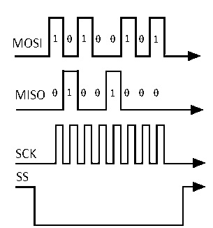
In the course of studying the AD9993-EBZ, it was found that only 8 data bits are used in the available 12-bit register address space. Also, the transmitted value of the register state is described by 8 bits. To determine the type of data transfer (write / read), it is required to transfer 1 data bit.
Since the current limitation on the maximum size of a message over the UART interface is 8 data bits, it was decided to transmit 3 consecutive 8-bit messages during the write process and 2 messages during the reading process.
The first package will contain the type of data transmission, duplicated for the entire package size. Therefore, there can be only two possible values: 00000000 for reading and 11111111 for writing, respectively. The use of an integer burst for the transmission of one data bit was done to simplify further processing of the received signals.
Next, the address of the requested register and the transmitted value of the register state during the recording process are transmitted.
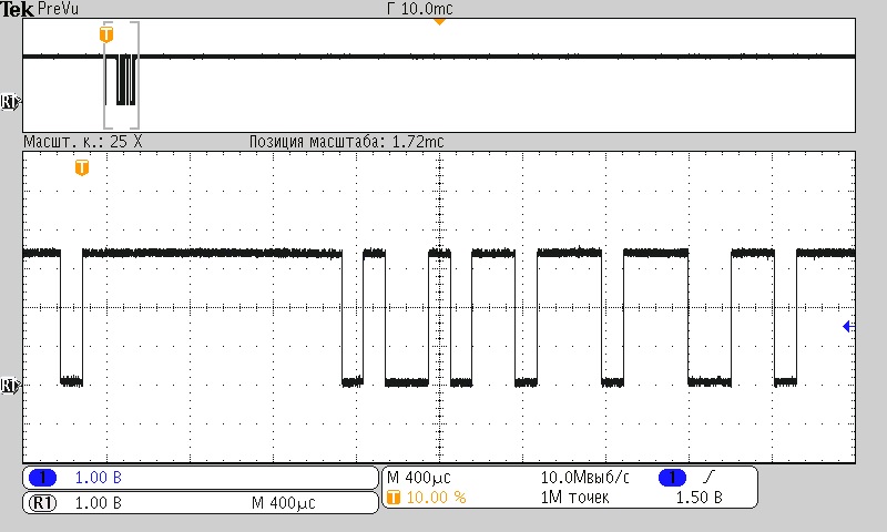
Oscillogram of the developed UART package
User interface

The main elements of the software user interface are buttons for connecting / disconnecting from available serial ports (elements 3,4), fields for entering the address and register values (elements 7,8), a log window (element 6). The software is designed to interact with it in two states: "connected to the port" and "disconnected from the port". States determine the activity of some elements on the program interface, and also restrict the execution of certain methods in order to reduce the probability of errors and incorrect software use. When enabled, the program is in the "disconnected from the port" state. Also, in order to facilitate work with the program (which I was one of the main goals of the project), the functionality of connecting files with already saved commands in JSON format was added (element 10).
Command loading process:

File selection

Commands interface The
functionality allows you to sort the loaded commands into sections (element 12), customize the process of working with connected commands (whether to send a command to the serial port immediately when pressed, or fill in the address fields and values in accordance with the selected command) ...
Development of a project for FPGA
general information
Before you start developing a project for an FPGA, you need to decide on the task that he must solve.
It sounds something like this: the project for the FPGA must support the following data conversion: Data conversion

diagram
The DE10-Nano receives signals from the Tx line of the UART interface (upper signal). Next, the FPGA needs to correctly determine the received data from three messages of 8 bits each and convert them into the SPI message format corresponding to the documentation (presented in 4 lines).
The main modules required to implement this conversion are a UART controller module and an SPI controller module. It is to them that the remainder of the chapter is assigned.
When developing projects for FPGAs, the IDE Qartus Prime Lite Edition 17th version was used.
If you have no experience using Quartus or have not programmed FPGAs at all, it is recommended to start with a clear (in my opinion) example of the first project on Quartus.
I would like to note that all the extracts from the Verilog code described below are a compilation of solutions found on the Internet that do not claim to be original. Again, the main goal of this project is to solve a specific problem.
UART controller
Description
The UART controller consists of three modules:
- pulse generator;
- recording module;
- reading module.
It is recommended to look at this article , from which most of the information was taken. From now on I will focus only on the most important (in my opinion) implementation details.
Pulse generator
Since the UART interface is asynchronous, the receiver needs to generate its own reference signal to correctly receive the transmitted signal, which allows it to correctly determine the beginning of a new bit of information.
There is a generally accepted range of standard UART baud rates: 300; 600; 1200; 2400; 4800; 9600; 19200; 38400; 57600; 115200; 230400; 460800; 921600 baud In our case, data transfer occurs at 9600 baud. Next, we need to get a generator with a frequency 16 times the symbol rate. This is necessary in order to correctly detect the level of the transmitted signal.
To generate pulses, a 50 MHz generator is used on the chip. To obtain the desired frequency, it is required to take into account every 325th pulse of the generator.
This is how it will look in Verilog:
input           Clk;                   //   50
input           Rst_n;               //
input [15:0]    BaudRate;      //   ,  325
output          Tick;                //
reg [15:0]      baudRateReg; //

always @(posedge Clk or negedge Rst_n)
    if (!Rst_n) baudRateReg <= 16'b1;
    else if (Tick) baudRateReg <= 16'b1;
         else baudRateReg <= baudRateReg + 1'b1;
assign Tick = (baudRateReg == BaudRate);
endmodule
Reader module
The reader converts the input signal from the RX line into an output 8-bit data array.
Directly reading and transferring the read data to the output:
input Clk, Rx,Tick;  //   50,  Rx,
input [3:0]NBits;                  //     ,  8
output RxDone;	         //
output [7:0]RxData;                         //

reg  read_enable = 1'b0;                   //
reg  RxDone = 1'b0;                         //
reg [3:0] counter = 4'b0000;            //
reg  start_bit = 1'b1;	                      //
reg [4:0]Bit = 5'b00000;                  //
reg [7:0] RxData;                            //
reg [7:0] Read_data= 8'b00000000; //


always @ (posedge Tick)  //
	begin
	if (read_enable)
	begin
	RxDone <= 1'b0;			//
	counter <= counter+1'b1;		//


	if ((counter == 4'b1000) & (start_bit))	//
	begin
	start_bit <= 1'b0;
	counter <= 4'b0000;
	end

	if ((counter == 4'b1111) & (!start_bit) & (Bit < NBits)) //
	begin
	Bit <= Bit+1'b1;
	Read_data <= {Rx,Read_data[7:1]};
	counter <= 4'b0000;
	end

	if ((counter == 4'b1111) & (Bit == NBits)  & (Rx))  //
	begin
	Bit <= 4'b0000;
	RxDone <= 1'b1;          //
	counter <= 4'b0000;          //
	start_bit <= 1'b1;		//
	end
	end

end


always @ (posedge Clk)
begin

if (NBits == 4'b1000)            //  8  ,
begin
RxData[7:0] <= Read_data[7:0];
end

end
Transmission module
The transmission module converts the 8-bit input signal into a UART serial data packet.
Direct data transfer:
input Clk, Rst_n, TxEn;  // 50,  ,
input Tick;                    //
input [3:0]NBits;          //
input [7:0]TxData;

output Tx;
output TxDone;

reg  Tx;
reg  TxDone = 1'b0;
reg write_enable = 1'b0;
reg start_bit = 1'b1;
reg stop_bit = 1'b0;
reg [4:0] Bit = 5'b00000;
reg [3:0] counter = 4'b0000;
reg [7:0] in_data=8'b00000000;

always @ (posedge Tick)  //
begin

	if (!write_enable)
	begin
	TxDone = 1'b0;
	start_bit <=1'b1;
	stop_bit <= 1'b0;
	end

	if (write_enable)
	begin
	counter <= counter+1'b1;	//

	if(start_bit & !stop_bit)//
	begin
	Tx <=1'b0;
	in_data <= TxData;

	if ((counter == 4'b1111) & (start_bit) )    //
	begin
	start_bit <= 1'b0;
	in_data <= {1'b0,in_data[7:1]};
	Tx <= in_data[0];
	end

	if ((counter == 4'b1111) & (!start_bit) &  (Bit < NBits-1))	//
	begin
	in_data <= {1'b0,in_data[7:1]};
	Bit<=Bit+1'b1;
	Tx <= in_data[0];
	start_bit <= 1'b0;
	counter <= 4'b0000;
	end

	if ((counter == 4'b1111) & (Bit == NBits-1) & (!stop_bit))	//
	begin
	Tx <= 1'b1;
	counter <= 4'b0000;
	stop_bit<=1'b1;
	end

	if ((counter == 4'b1111) & (Bit == NBits-1) & (stop_bit) )	//
	begin
	Bit <= 4'b0000;
	TxDone <= 1'b1;
	counter <= 4'b0000;
	//start_bit <=1'b1;
	end

	end

end
SPI controller
Important digression
Since the SPI controller, implemented on the basis of an FPGA, is a more complex logical structure than the UART controller, the further explanation of the operation logic is easier to carry out on the circuit model of the controller.
General scheme of the controller

The developed model can be divided into 3 main modules:
- sequential write module;
- bit counter module;
- error analyzer module.
The division into modules is rather arbitrary, since the circuit has high connectivity between the elements used. The division is based on the tasks performed by individual groups of elements, presented in the general diagram.
The clocking of the circuit is provided by a 12.5 MHz signal supplied through the CLK_125 line.
The start of the controller's work on the formation of a control message is carried out by the "START" signal. By this signal, all modules of the circuit are set to their initial state and the beginning of the cycle of generating the required signals on the output lines CLK, SS, MOSI of the SPI interface is initialized
Sequential write module

The serial write module will perform the main task of the SPI controller, namely, the output of parallel bit data to the serial MOSI line. This is due to the RG_24_PI_SO element, which operates on the principle of a shift register based on D-flip-flops.
The RG_24_PI_SO element has 24 data inputs corresponding to the AD9993-EBZ documentation on the SPI send format. They include:
- Command data (DATA_0 – DATA_7);
- Register address data (ADR_0 – ADR_12);
- W / R write / read mode bit.
The presented signals are written in parallel at a logic level "1" at the LoadP_ShiftN input. Further, at the logic level "0" at the LoadP_ShiftN input, at each clock cycle at the CLK input, the element alternately reproduces the recorded data to the serial line of the MOSI output.
Bit counter module
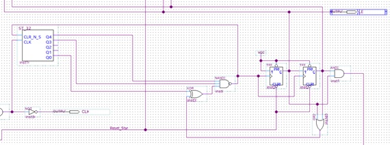
The bit counter module is required to determine the duration of the data write enable signal on the SS line of the SPI interface. Since, according to the AD9993-EBZ documentation, the duration of the enable signal must be equal to the total duration of the transmitted data, it becomes necessary to count 24 sync pulses from the beginning of data transmission to determine the required duration of the enable signal. The counting function is performed by the ST_32 element, which, when the 24th clock signal is detected, reproduces a signal that is used to reset the counter, as well as to end the transmitted enable signal.
In addition to the main functionality, the bit counter module is also responsible for initializing the error analysis process, the initial action of which is to send the read value command to the address of the last recorded register. Since the error analysis process must be started after a time interval equivalent to the duration of 23 sync pulses from the moment the last transmitted data bit was transmitted (established experimentally), the bit counter after the reset signal switches to the 23 sync pulse counting mode, which ensures the operation of the error analysis process.
Error analysis module

As mentioned in the explanation of the previous module, to provide the functionality of error analysis, a method was developed based on reading the value of the command stored on the IC at the register address used in the data recording process. The reading process is necessary to compare the written value with the read data to identify inconsistencies, and therefore to determine the error that occurred. The error analysis module is based on the RG_8_SI_PO element, which operates on the principle of a shift register. The element converts the signals received via the MISO serial port into a parallel 8-bit output. Then the data is compared with the value of the command used during the data recording process. The comparison functionality is performed by the CMP_8 element based on the exclusive-or logic. If a discrepancy is found,the module sends a signal to the LED output, which will be in the state of a logical unit until the next data recording process. It is assumed that the LED output will be connected to one of the LEDs, a group of which is present on the DE10 Nano development board, which will visually signal an error that has occurred.
Conclusion
As a result of solving this problem, the scheme of interaction between the PC and the DAC / ADC device was designed and physically implemented with a number of key advantages. In the process of implementation, the problem with the connection of the FPGA and PC was solved. The solution to this was to use an external UART module. PC software was written in Java. The software has an interface with basic capabilities for transmitting and receiving data in the developed UART sending format, in addition, it has the function of loading saved commands. FPGA-based UART and SPI controllers were developed.
The issues considered within the framework of this project allow:
- evaluate the ways of interaction of integrated circuits with external devices;
- evaluate ways of using FPGAs as a matching device, a buffer for data exchange;
- explore one of the most effective approaches to developing software for practical use.
PS I will be glad to any additions, remarks and indications of mistakes.