KDPV. Tiger Lake laptop prototype.
Brief summary
Most of the leaked information is intended for OEM / ODM developers and manufacturers, but will be of interest to enthusiasts researching BIOS and undocumented modes of Intel processors. They do not contain internal Intel documentation, critical to the release, or capable of revealing secret developments. Also, you will not find information about previously unknown vulnerabilities here.
Files
Files not listed here are either just Intel news updates, undescribed binaries, or not worthy of attention.
File 576931-potter-city-576931-v1-0-schem.pdf
Diagrams, wiring diagrams, layout recommendations for motherboards with four sockets for processors on the SandyBridge core from 2010.
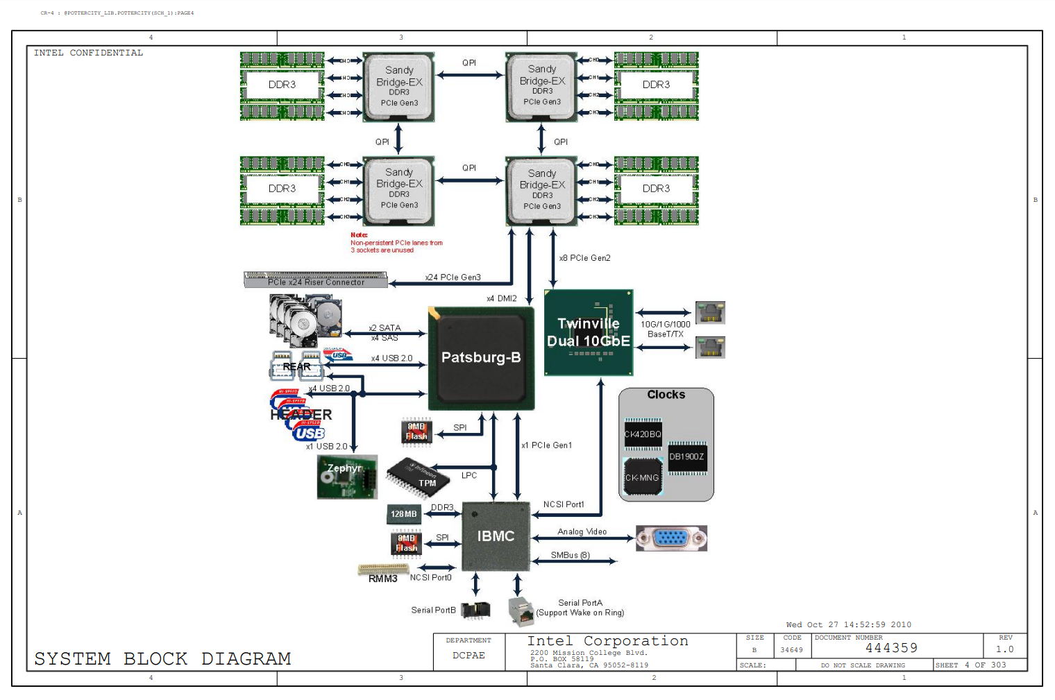
Interestingly, only the reassignable PCIe lanes of one processor are used.
The rest of the pages contain data for all blocks indicated in the diagram. It can be useful for academic knowledge; it will not work to transfer to real motherboards.

For example, blocking capacitors for different circuits showing the exact component labeling and placement
guidelines File 367228-367228-rev-1-5.pdf
Wiring documentation for something like a debug / demo board for the first generation of atoms.

Block diagram with explanations on the operation of the power circuit when turned on
File 544767-intel-ethernet-connection-i219-reference-schematic-rev1-0.pdf
Typical wiring diagram for a gigabit network adapter i219 , 2015.

File 555388-purley-platform-power-delivery-schematic-layout-checklist-rev1-1.xlsx
A spreadsheet for engineers or testers of third party boards. It is necessary to check the wiring diagram and topology (specifically the power section) for compliance with the recommended requirements. At the end, excel will calculate the "points" and give the result as a percentage:

File 621487-cml-itbmt3-ta-ww14-2020.pdf
General description of how Turbo Boost 3.0 works in Kaby Lake (this is the 7th generation Core from 2017). In particular, it is described from which processor registers the BIOS subsystem should read the maximum boost multipliers of individual cores.

File 20170823_HDCP_EB-1.0_MEDIA_Eng_release.tar.gz
Daemon and test utility for testing HDCP operation under Arch Linux. The archive contains only binaries and readme.
File BVT_Package_10.0.0.1086.exe
Utility and Documentation for verifying system compliance with Intel requirements for marking a computer with the Intel vPro logo . The utility runs several tests, and then a report can be sent to Intel if all tests pass.
File cmls102-prq-report-rev0.pdf
April 2020 Chip Test Methodology and Predicted Failure Rates for Core and Xeon Processors. From this document, you can find out what processors go through before getting into our computers:

Infant Mortality Test - this is the first test of microcircuits after packaging in operation at elevated temperatures. The name is not the most morally acceptable , but what to expect from the authors of master / slave?
More details about the microcircuit testing procedure can be found in the movie, which I will publish soon.
File prq-prq-customer-report-skl-2-2-lga-dt-rev0.pdf
Same report for Pentium and i3 processors from 2015.
File c-state-test-case-intel-soc-watch-bkc-626226-rev0-5.pdf
Testing options for c-state and p-state processor modes (optimization in terms of power consumption and frequency with voltage). Step-by-step instructions on BIOS settings and using a special testing utility.
File FMX.Data.Flows.Training.v1.0_2020-02-11_AVM.pdf
Some poorly laid out presentation on the topic of network transmission. It is half abbreviated, so I didn't know what it was exactly. 2020 year.
File glk_platform_intel®_txe_4.0.25.1324_mr.pdf
Some (incomplete) description of a set of utilities for building and signing firmware for the Intel TXE module . For example, there is a table of TXE components with their sizes and recommendations for choosing the capacity of the flash chip for the BIOS. 2020 year.
How to obtain intel system debugger nda.pdf file
Provides guidance for obtaining the Intel Processor Development Kit. Literally how and what fields to fill in the form on the site. 2020 year.
File qts-qpp-5v1-17-1.pdf
Instruction for Quartus Pro - software for development for FPGA (before the purchase by Intel it was known as Altera Quartus).
File SeamlessUpdate_CapsuleGeneration_UserGuide_v0.5.2.pdf
Instructions for hardware manufacturers to build patches for updating BIOS, Intel ME, microcode and the like.
File SeamlessUpdate_CapsuleGenerationEnv_v0.5.2.zip
The set of utilities for assembly.
Simicsmodellibrary_eaglestream_rn_v0_6_00.pdf
Brief instructions for installing and using the system emulation utility. It is used in the development of BIOS firmware for processors not yet released.
Folder Intel ME Contains utilities, documentation and binaries for Intel ME . Absolutely nothing useful was found. There is a source code for an example utility for flashing, but it uses the FWUpdateLib.lib C library, which does all the interesting work. In the code in all functions, there is a kind of exit from functions by goto (the End label is the same in all functions), nothing more remarkable.
View listing
static UINT32 checkUpdateType(IN  const char *fileName, IN  UINT32 *updateType)
{
    UINT32 status;
    UINT16 flashMajor = 0;
    UINT16 flashMinor = 0;
    UINT16 flashHotfix = 0;
    UINT16 flashBuild = 0;
    UINT16 fileMajor = 0;
    UINT16 fileMinor = 0;
    UINT16 fileHotfix = 0;
    UINT16 fileBuild = 0;
    INT32  comparedVersion = 0;

    if (fileName == NULL || updateType == NULL)
    {
        status = INTERNAL_ERROR;
        goto End;
    }

    status = FwuPartitionVersionFromFlash(FPT_PARTITION_NAME_FTPR, &flashMajor, &flashMinor, &flashHotfix, &flashBuild);
    if (status != SUCCESS)
    {
        goto End;
    }

    status = FwuPartitionVersionFromFile(fileName, FPT_PARTITION_NAME_FTPR, &fileMajor, &fileMinor, &fileHotfix, &fileBuild);
    if (status != SUCCESS)
    {
        goto End;
    }

    comparedVersion = versionCompare(fileMajor, fileMinor, fileHotfix, fileBuild,
                                     flashMajor, flashMinor, flashHotfix, flashBuild);

    if (comparedVersion < 0)
    {
        *updateType = DOWNGRADE;
    }
    else if (comparedVersion > 0)
    {
        *updateType = UPGRADE;
    }
    else
    {
        *updateType = SAME_VERSION;
    }

End:
    return status;
}
Intel Restricted Secret folder
And here is already something interesting. The KabylakePlatform_3_7_9 \ KabylakePlatSamplePkg folder contains an example BIOS for the Kaby Lake platform (this is the 7th generation of Core processors, released in 2017). I did not try to collect it, but it looks like it has everything you need.

The Features folder contains the source code for device drivers For example, for SATA, in appearance, it is quite a working code for searching and initializing a device on PCIe.

Listing
/**
  This routine is called right after the .Supported() is called and returns
  EFI_SUCCESS. Notes: The supported protocols are checked but the Protocols
  are closed.

  @param[in] This                 A pointer points to the Binding Protocol instance
  @param[in] Controller           The handle of controller to be tested. Parameter
                                  passed by the caller
  @param[in] RemainingDevicePath  A pointer to the device path. Should be ignored by
                                  device driver

  @retval EFI_SUCCESS             The device is started
  @retval Other values            Something error happened
**/
EFI_STATUS
EFIAPI
SataControllerStart (
  IN EFI_DRIVER_BINDING_PROTOCOL    *This,
  IN EFI_HANDLE                     Controller,
  IN EFI_DEVICE_PATH_PROTOCOL       *RemainingDevicePath
  )
{
  EFI_STATUS                        Status;
  EFI_IDE_CONTROLLER_INIT_PROTOCOL  *IdeInit;
  EFI_PCI_IO_PROTOCOL               *PciIo;
  UINT8                             NumberOfPort;
  UINT64                            CommandVal;

  DEBUG ((DEBUG_INFO, "SataControllerStart() Start\n"));

  ///
  /// Now test and open the EfiPciIoProtocol
  ///
  Status = gBS->OpenProtocol (
                  Controller,
                  &gEfiPciIoProtocolGuid,
                  (VOID **) &PciIo,
                  This->DriverBindingHandle,
                  Controller,
                  EFI_OPEN_PROTOCOL_BY_DRIVER
                  );
  ///
  /// Status == 0 - A normal execution flow, SUCCESS and the program proceeds.
  /// Status == ALREADY_STARTED - A non-zero Status code returned. It indicates
  ///           that the protocol has been opened and should be treated as a
  ///           normal condition and the program proceeds. The Protocol will not
  ///           opened 'again' by this call.
  /// Status != ALREADY_STARTED - Error status, terminate program execution
  ///
  if (EFI_ERROR (Status)) {
    ///
    /// EFI_ALREADY_STARTED is also an error
    ///
    return Status;
  }

  ///
  /// Get device capabilities
  ///
  Status = PciIo->Attributes (
                    PciIo,
                    EfiPciIoAttributeOperationSupported,
                    0,
                    &CommandVal
                    );
  ASSERT_EFI_ERROR (Status);

  ///
  /// Enable Command Register
  ///
  Status = PciIo->Attributes (
                    PciIo,
                    EfiPciIoAttributeOperationEnable,
                    CommandVal & EFI_PCI_DEVICE_ENABLE,
                    NULL
                    );
  ASSERT_EFI_ERROR (Status);

  ///
  /// Get Number of Ports
  ///
  PciIo->Mem.Read (
               PciIo,
               EfiPciIoWidthUint8,
               EFI_AHCI_BAR_INDEX,
               (UINT64) R_AHCI_CAPABILITY,
               1,
               & NumberOfPort
               );
  NumberOfPort = (NumberOfPort & 0x1F) + 1;

  IdeInit = AllocatePool (sizeof (EFI_IDE_CONTROLLER_INIT_PROTOCOL));
  if (IdeInit == NULL) {
    return EFI_OUT_OF_RESOURCES;
  }
  IdeInit->GetChannelInfo = IdeInitGetChannelInfo;
  IdeInit->NotifyPhase    = IdeInitNotifyPhase;
  IdeInit->SubmitData     = IdeInitSubmitData;
  IdeInit->DisqualifyMode = IdeInitDisqualifyMode;
  IdeInit->CalculateMode  = IdeInitCalculateMode;
  IdeInit->SetTiming      = IdeInitSetTiming;
  IdeInit->EnumAll        = SATA_ENUMER_ALL;
  IdeInit->ChannelCount   = NumberOfPort;

  ///
  /// Install IDE_CONTROLLER_INIT protocol & private data to this instance
  ///
  Status = gBS->InstallMultipleProtocolInterfaces (
                  &Controller,
                  &gEfiIdeControllerInitProtocolGuid,
                  IdeInit,
                  NULL
                  );

  ///
  /// Close protocols opened by SATA controller driver
  ///
  gBS->CloseProtocol (
        Controller,
        &gEfiPciIoProtocolGuid,
        This->DriverBindingHandle,
        Controller
        );

  DEBUG ((DEBUG_INFO, "SataControllerStart() End\n"));

  return Status;
}
Also in the Intel Restricted Secret folder are the sources:
- Initialization codes for Kaby Lake processors with documentation;
- Something called Client Silicon API package;
- Instructions for integrating all this into your BIOS (for hardware developers).
File 482486-crystal-forest-gladden-stargo-schematic-design-files-rev2-1.zip Cadence
libraries for development for Intel platform codenamed Crystal Forest . There are no projects with board routing. EEPROM logic Discrete components Connectors Common set of libraries. Most likely from the Cadence distribution package. The files themselves are dated 2012. File 555146-kipsbay2-archive.zip Same for arduino compatible Intel Galileo boards . Also without trace files. File 607872-tgl-up3-up4-pdg-schchk-rev1-2.zip


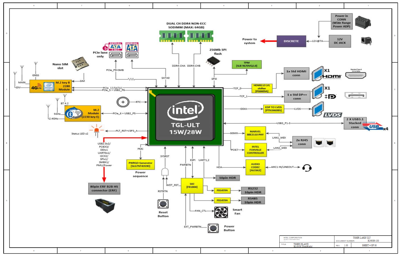
Very detailed instructions for developing wiring diagrams and tracing boards for the 11th generation Core processors that have not yet been released, codenamed Tiger Lake.

There are many such illustrative illustrations with explanations.
File 615188-wilson-city-schematic-walkthrough-bmc.zip
Video presentation with explanations to the diagram of a chipset codenamed Wilson City. Soundtrack by voice synthesizer.

Still from this exciting video
File 615704-cml-s-udimm-3200-cmp-h-rvp-tdk-rev0p7.zip Wiring diagrams
and Cadence project with traces of a typical board for Comet Lake S processors with UDIMM memory.

Nice 10 layers

Level converter for HDMI
File 618525-tigerlake-up3-tsn-aic.zip
It looks like a wiring diagram and a description of a test board with peripherals for the yet-to-be-released Tiger Lake processor.

PCIe board with two Ethernet controllers and PHY for them.

Explanations of changes in this revision
File 618730-ehl-mcl-hierarchical-schematic-lp4x-0-7.zip
Cadence component library for not yet released Elkhart Lake processors (Intel Atom line). No project files, but complete wiring diagram for all peripherals and power supply. You can already estimate which ports will be on the board.

File adk_source.2.0.11.09.standalone.snowridge_transportip.tar.gz
Source codes and instructions for the utility for emulating the network subsystem of not yet released Snowfish processors... As I understand it, it connects to the Snowfish processor emulator and allows you to test network capabilities.
File aml_cfl_s_kbl_skl-vbios_9.0.1062.zip
Some script for a VBIOS editing utility for OEM developers. The structure of the VBIOS firmware file is described in text form.
File apl-i_sic_1.1.1_v227_51_d20190502.zip Apollo Lake
processor initialization code sources and documentation. File core 10x00k 10x00kf v 1.0.5.zip Contains an installer for a utility with a very promising name: I don't have such a processor, so I couldn't check it. Elkhartlake_silicon_and_platformsamplecode_v1.0.0.zip file

The sources of the initialization codes are now for Elkhart Lake, with a part of the sources for the BIOS and the Client Silicon. I suspect you can use the Kaby Lake sample BIOS to build the BIOS for these processors.
Intel®pch chipset_init kit file - tglpchlp_z0v5_a0v11.zip
BIOS patch in binary form and instructions for the utility for installing this patch into the firmware. The patch itself fixes some errors in the initialization of the chipset for Tiger Lake processors.
Intel®powerandthermaldesignstudio_ext_2.1.1.zip
Intel Power and Thermal Design Studio cryptic utility.

KBL SST FDK training session 2.1.zip files - KBL SST FDK training session 4.2.zip
Recording video tutorials on developing either firmware, or drivers in some kind of graphical utility. The voice of a Hindu with a bad pronunciation is heard off-screen.
File main_pld_adr_engineering_release_ww19.zip
Verilog -codes for the already mentioned Wilson City chipset. Apparently for testing in FPGAs before fabrication in silicon.
Very long listing
// (C) 2020 Intel Corporation. All rights reserved.
// Your use of Intel Corporation's design tools, logic functions and other
// software and tools, and its AMPP partner logic functions, and any output
// files from any of the foregoing (including device programming or simulation
// files), and any associated documentation or information are expressly subject
// to the terms and conditions of the Intel Program License Subscription
// Agreement, Intel FPGA IP License Agreement, or other applicable
// license agreement, including, without limitation, that your use is for the
// sole purpose of programming logic devices manufactured by Intel and sold by
// Intel or its authorized distributors. Please refer to the applicable
// agreement for further details.
`timescale 1ns/1ns
`define dedicated_debug_logic
module Wilson_City_Main (
// Input CLK
input iClk_2M,
input iClk_50M,
output o1mSCE,
//GSX Interface with BMC
input SGPIO_BMC_CLK,
input SGPIO_BMC_DOUT,
output SGPIO_BMC_DIN,
input SGPIO_BMC_LD_N,
//I2C Support
inout SMB_PLD_SDA, // SMB_PCH_PMBUS2_STBY_LVC3_SDA
input SMB_PLD_SCL, // SMB_PCH_PMBUS2_STBY_LVC3_SCL
output onSDAOE,
//LED and 7-Seg Control Logic
output [7:0] LED_CONTROL,
output FM_CPU1_DIMM_CH1_4_FAULT_LED_SEL,
output FM_CPU1_DIMM_CH5_8_FAULT_LED_SEL,
output FM_CPU2_DIMM_CH1_4_FAULT_LED_SEL,
output FM_CPU2_DIMM_CH5_8_FAULT_LED_SEL,
output FM_FAN_FAULT_LED_SEL_N,
output FM_POST_7SEG1_SEL_N,
output FM_POST_7SEG2_SEL_N,
output FM_POSTLED_SEL,
//CATERR DLY
output FM_CPU_CATERR_DLY_LVT3_N,
input FM_CPU_CATERR_PLD_LVT3_N, //% No Input FF
//ADR
input FM_ADR_COMPLETE, //% Input FF
output FM_ADR_COMPLETE_DLY,
output FM_ADR_SMI_GPIO_N,
inout FM_ADR_TRIGGER_N,
input FM_PLD_PCH_DATA, //% Input FF
input FM_PS_PWROK_DLY_SEL, //% Input FF
input FM_DIS_PS_PWROK_DLY, //% Input FF
//ESPI Support
output FM_PCH_ESPI_MUX_SEL,
//System THROTTLE
input FM_PMBUS_ALERT_B_EN, //% Input FF
input FM_THROTTLE_N, //% Input FF
input IRQ_SML1_PMBUS_PLD_ALERT_N, //% Input FF
output FM_SYS_THROTTLE_LVC3_PLD,
// Termtrip dly
input FM_CPU1_THERMTRIP_LVT3_PLD_N, //% Input FF
input FM_CPU2_THERMTRIP_LVT3_PLD_N, //% Input FF
input FM_MEM_THERM_EVENT_CPU1_LVT3_N, //% Input FF
input FM_MEM_THERM_EVENT_CPU2_LVT3_N, //% Input FF
output FM_THERMTRIP_DLY,
//MEMHOT
input IRQ_PVDDQ_ABCD_CPU1_VRHOT_LVC3_N,//% Input FF
input IRQ_PVDDQ_EFGH_CPU1_VRHOT_LVC3_N,//% Input FF
input IRQ_PVDDQ_ABCD_CPU2_VRHOT_LVC3_N,//% Input FF
input IRQ_PVDDQ_EFGH_CPU2_VRHOT_LVC3_N,//% Input FF
output FM_CPU1_MEMHOT_IN,
output FM_CPU2_MEMHOT_IN,
//MEMTRIP
input FM_CPU1_MEMTRIP_N, //% Input FF
input FM_CPU2_MEMTRIP_N, //% Input FF
//PROCHOT
input FM_PVCCIN_CPU1_PWR_IN_ALERT_N, //% Input FF
input FM_PVCCIN_CPU2_PWR_IN_ALERT_N, //% Input FF
input IRQ_PVCCIN_CPU1_VRHOT_LVC3_N, //% Input FF
input IRQ_PVCCIN_CPU2_VRHOT_LVC3_N, //% Input FF
output FM_CPU1_PROCHOT_LVC3_N,
output FM_CPU2_PROCHOT_LVC3_N,
//PERST & RST
input FM_RST_PERST_BIT0, //% No-Input FF
input FM_RST_PERST_BIT1, //% No-Input FF
input FM_RST_PERST_BIT2, //% No-Input FF
output RST_PCIE_PERST0_N,
output RST_PCIE_PERST1_N,
output RST_PCIE_PERST2_N,
output RST_CPU1_LVC3_N,
output RST_CPU2_LVC3_N,
output RST_PLTRST_B_N,//RST_PLTRST_PLD_B_N
input RST_PLTRST_N, //RST_PLTRST_PLD_N //% Input FF
//FIVR
input FM_CPU1_FIVR_FAULT_LVT3, //FM_CPU1_FIVR_FAULT_LVT3_PLD //% Input FF
input FM_CPU2_FIVR_FAULT_LVT3, //FM_CPU2_FIVR_FAULT_LVT3_PLD //% Input FF
//CPU Misc
input FM_CPU1_PKGID0, //% No-Input FF
input FM_CPU1_PKGID1, //% No-Input FF
input FM_CPU1_PKGID2, //% No-Input FF
input FM_CPU1_PROC_ID0, //% No-Input FF
input FM_CPU1_PROC_ID1, //% No-Input FF
input FM_CPU1_INTR_PRSNT, //% No-Input FF
input FM_CPU1_SKTOCC_LVT3_N, //FM_CPU1_SKTOCC_LVT3_PLD_N //% No-Input FF
input FM_CPU2_PKGID0, //% No-Input FF
input FM_CPU2_PKGID1, //% No-Input FF
input FM_CPU2_PKGID2, //% No-Input FF
input FM_CPU2_PROC_ID0, //% No-Input FF
input FM_CPU2_PROC_ID1, //% No-Input FF
input FM_CPU2_INTR_PRSNT, //% No-Input FF
input FM_CPU2_SKTOCC_LVT3_N, //FM_CPU2_SKTOCC_LVT3_PLD_N //% No-Input FF
//BMC
input FM_BMC_PWRBTN_OUT_N, //% Input FF
input FM_BMC_ONCTL_N, //FM_BMC_ONCTL_N_PLD //% Input FF
output RST_SRST_BMC_PLD_N, //RST_SRST_BMC_PLD_R_N
output FM_P2V5_BMC_EN, //FM_P2V5_BMC_EN_R
input PWRGD_P1V1_BMC_AUX, //% Input FF
//PCH
output RST_RSMRST_N, // RST_RSMRST_PLD_R_N
output PWRGD_PCH_PWROK, // PWRGD_PCH_PWROK_R
output PWRGD_SYS_PWROK, // PWRGD_SYS_PWROK_R
input FM_SLP_SUS_RSM_RST_N, //% Input FF
input FM_SLPS3_N, // FM_SLPS3_PLD_N //% Input FF
input FM_SLPS4_N, // FM_SLPS4_PLD_N //% Input FF
input FM_PCH_PRSNT_N, //% No-Input FF
output FM_PCH_P1V8_AUX_EN, // FM_PCH_P1V8_AUX_EN_R
input PWRGD_P1V05_PCH_AUX, //% Input FF
input PWRGD_P1V8_PCH_AUX, // PWRGD_P1V8_PCH_AUX_PLD //% Input FF
output FM_PFR_MUX_OE_CTL_PLD, //% PFR Mux Sel
input RST_DEDI_BUSY_PLD_N, //% Dediprog RST
//PSU Ctl
output FM_PS_EN, // FM_PS_EN_PLD_R
input PWRGD_PS_PWROK, // PWRGD_PS_PWROK_PLD_R //% Input FF
//Clock Logic
output FM_PLD_CLKS_OE_N,// FM_PLD_CLKS_OE_R_N
output FM_CPU_BCLK5_OE_R_N,
//Base Logic
input PWRGD_P3V3_AUX, //PWRGD_P3V3_AUX_PLD_R //% Input FF
//Main VR & Logic
input PWRGD_P3V3, //% Input FF
output FM_P5V_EN,
output FM_AUX_SW_EN,
//Mem
input PWRGD_CPU1_PVDDQ_ABCD, //% Input FF
input PWRGD_CPU1_PVDDQ_EFGH, //% Input FF
input PWRGD_CPU2_PVDDQ_ABCD, //% Input FF
input PWRGD_CPU2_PVDDQ_EFGH, //% Input FF
output FM_PVPP_CPU1_EN,
output FM_PVPP_CPU2_EN,
//CPU
output PWRGD_CPU1_LVC3,
output PWRGD_CPU2_LVC3,
input PWRGD_CPUPWRGD, //PWRGD_CPUPWRGD_PLD_R //% Input FF
output PWRGD_DRAMPWRGD_CPU,
output FM_P1V1_EN, // Used to turn on PCIE re-timmer vr
output FM_P1V8_PCIE_CPU1_EN,
output FM_P1V8_PCIE_CPU2_EN,
output FM_PVCCANA_CPU1_EN,
output FM_PVCCANA_CPU2_EN,
output FM_PVCCIN_CPU1_EN,
output FM_PVCCIN_CPU2_EN,
output FM_PVCCIO_CPU1_EN,
output FM_PVCCIO_CPU2_EN,
output FM_PVCCSA_CPU1_EN,
output FM_PVCCSA_CPU2_EN,
input PWRGD_BIAS_P1V1, //% Input FF
input PWRGD_P1V8_PCIE_CPU1, //% Input FF
input PWRGD_P1V8_PCIE_CPU2, //% Input FF
input PWRGD_PVCCIN_CPU1, //% Input FF
input PWRGD_PVCCIN_CPU2, //% Input FF
input PWRGD_PVCCIO_CPU1, //% Input FF
input PWRGD_PVCCIO_CPU2, //% Input FF
input PWRGD_PVCCSA_CPU1, //% Input FF
input PWRGD_PVCCSA_CPU2, //% Input FF
input PWRGD_VCCANA_PCIE_CPU1, //% Input FF
input PWRGD_VCCANA_PCIE_CPU2, //% Input FF
//DBP
input DBP_POWER_BTN_N, //% Input FF
input DBP_SYSPWROK, //DBP_SYSPWROK_PLD //% Input FF
//Debug
input FM_FORCE_PWRON_LVC3,
output FM_PLD_HEARTBEAT_LVC3,
// Front Panel
output FP_LED_FAN_FAULT_PWRSTBY_PLD_N, // Emeral ridge support
output FP_BMC_PWR_BTN_CO_N, // need add support OD
//Debug pins I/O
output SGPIO_DEBUG_PLD_CLK,
input SGPIO_DEBUG_PLD_DIN,
output SGPIO_DEBUG_PLD_DOUT,
output SGPIO_DEBUG_PLD_LD_N,
input SMB_DEBUG_PLD_SCL,
input SMB_DEBUG_PLD_SDA,
output oSMB_DEBUG_PLD_SDA_OE,
input FM_PLD_REV_N,
input SPI_BMC_BOOT_R_CS1_N,
output SPI_PFR_BOOT_CS1_N
);
//////////////////////////////////////////////////////////////////////////////////
// Parameters
//////////////////////////////////////////////////////////////////////////////////
parameter LOW =1'b0;
parameter HIGH=1'b1;
parameter FPGA_MAJOR_REV = 8'd00;
parameter FPGA_MINOR_REV = 8'd06;
parameter FPGA_DEBUG_MINIMUM_MAJOR_REV = 8'd00;
parameter FPGA_DEBUG_MINIMUM_MINOR_REV = 8'd01;
//////////////////////////////////////////////////////////////////////////////////
// Internal Signals
//////////////////////////////////////////////////////////////////////////////////
wire wCLK_20mSCE, wCLK_250mS, wCLK1SCE;
wire w1uSCE;
wire w5uSCE;
wire w10uSCE;
wire w500uSCE;
wire w1mSCE;
wire w250mSCE;
wire w20mSCE;
wire w1SCE;
wire wvRstPCIePERst_n [2:0];
wire wRstPchPerstN,wRstCPU0PerstN,wRstCPU1PerstN;
wire wPsuPwrEn,wPsuPwrFlt,wPsuPwrgd,wPwrgd_Ps_Pwrok_Dly;
wire wRst_n, wMemPwrEn;
wire wBmcPwrgd,wBmcPwrFlt;
wire wPchPwrgd,wPchPwrFlt;
wire wMemPwrgd,wMemPwrFlt;
wire wCpuPwrEn,wCpuPwrgd,wCpuPwrFlt;
wire wFault;
wire wTimeout;
wire [2:0] wDbgMemSt_CPU1;
wire [2:0] wDbgMemSt_CPU2;
wire [3:0] wDbgCpuSt_CPU1;
wire [3:0] wDbgCpuSt_CPU2;
wire [3:0] wDbgMstSt;
wire [3:0] wDbgMstSt7Seg;
wire [3:0] wFaultStage;
wire [7:0] wFaultState;
wire [254:0] wMonitorFaultState;
wire wGoOutFltSt;
wire FM_THROTTLE_N_FF;
wire IRQ_SML1_PMBUS_PLD_ALERT_N_FF;
wire FM_CPU1_THERMTRIP_LVT3_PLD_N_FF;
wire FM_CPU2_THERMTRIP_LVT3_PLD_N_FF;
wire FM_MEM_THERM_EVENT_CPU1_LVT3_N_FF;
wire FM_MEM_THERM_EVENT_CPU2_LVT3_N_FF;
wire IRQ_PVDDQ_ABCD_CPU1_VRHOT_LVC3_N_FF;
wire IRQ_PVDDQ_EFGH_CPU1_VRHOT_LVC3_N_FF;
wire IRQ_PVDDQ_ABCD_CPU2_VRHOT_LVC3_N_FF;
wire IRQ_PVDDQ_EFGH_CPU2_VRHOT_LVC3_N_FF;
wire FM_CPU1_MEMTRIP_N_FF;
wire FM_CPU2_MEMTRIP_N_FF;
wire FM_PVCCIN_CPU1_PWR_IN_ALERT_N_FF;
wire FM_PVCCIN_CPU2_PWR_IN_ALERT_N_FF;
wire IRQ_PVCCIN_CPU1_VRHOT_LVC3_N_FF;
wire IRQ_PVCCIN_CPU2_VRHOT_LVC3_N_FF;
wire FM_BMC_PWRBTN_OUT_N_FF;
wire FM_BMC_ONCTL_N_FF;
wire FM_SLP_SUS_RSM_RST_N_FF;
wire DBP_POWER_BTN_N_FF;
wire RST_PLTRST_N_FF;
wire FM_SLPS3_N_FF;
wire FM_SLPS4_N_FF;
wire PWRGD_P1V1_BMC_AUX_FF;
wire PWRGD_P1V8_PCH_AUX_FF;
wire PWRGD_P1V05_PCH_AUX_FF;
wire PWRGD_PS_PWROK_FF;
wire PWRGD_P3V3_AUX_FF;
wire PWRGD_P3V3_FF;
wire PWRGD_CPU1_PVDDQ_ABCD_FF;
wire PWRGD_CPU1_PVDDQ_EFGH_FF;
wire PWRGD_CPU2_PVDDQ_ABCD_FF;
wire PWRGD_CPU2_PVDDQ_EFGH_FF;
wire PWRGD_CPUPWRGD_FF;
wire PWRGD_BIAS_P1V1_FF;
wire PWRGD_P1V8_PCIE_CPU1_FF;
wire PWRGD_P1V8_PCIE_CPU2_FF;
wire PWRGD_PVCCIN_CPU1_FF;
wire PWRGD_PVCCIN_CPU2_FF;
wire PWRGD_PVCCIO_CPU1_FF;
wire PWRGD_PVCCIO_CPU2_FF;
wire PWRGD_PVCCSA_CPU1_FF;
wire PWRGD_PVCCSA_CPU2_FF;
wire PWRGD_VCCANA_PCIE_CPU1_FF;
wire PWRGD_VCCANA_PCIE_CPU2_FF;
wire FM_ADR_COMPLETE_FF;
wire FM_PLD_PCH_DATA_FF;
wire FM_PS_PWROK_DLY_SEL_FF;
wire FM_DIS_PS_PWROK_DLY_FF;
wire FM_PMBUS_ALERT_B_EN_FF;
wire FM_CPU1_FIVR_FAULT_LVT3_FF;
wire FM_CPU2_FIVR_FAULT_LVT3_FF;
wire DBP_SYSPWROK_FF;
wire wCPUPwrGd_Dly;
wire [7:0] wvPOSTCodeLEDs;
wire [7:0] wvFanFaultLEDs;
wire [15:0] wvP1DIMMLEDs;
wire [15:0] wvP2DIMMLEDs;
wire [15:0] wvP3DIMMLEDs;
wire [15:0] wvP4DIMMLEDs;
wire wvMCPSilicon;
wire wSocketRemoved;
wire wValidForcePowerOn;
wire wPWRGD_CPU_LVC3;
wire wPchPwrFltP1V05;
wire wPchPwrFltP1V8;
wire wSysOk;
wire wCPUMismatch;
wire wPWRGD_PS_PWROK_DLY;
wire wPWRGD_PS_PWROK_DLY_ADR;
wire wMainVRPwrEn;
wire wMainPwrFlt;
wire wP3v3PwrFlt;
wire wMainVRPwrgd;
wire wFM_AUX_SW_EN;
wire wFM_P5V_EN;
wire wMemPwrFltVDDQ_CPU1_ABCD;
wire wMemPwrFltVDDQ_CPU1_EFHG;
wire wMemPwrgd_CPU1;
wire wMemPwrFlt_CPU1;
wire wMemPwrFltVDDQ_CPU2_ABCD;
wire wMemPwrFltVDDQ_CPU2_EFHG;
wire wMemPwrgd_CPU2;
wire wMemPwrFlt_CPU2;
wire wCpuPwrgd_CPU1;
wire wCpuPwrFlt_CPU1;
wire wPWRGD_PVCCIO_CPU1;
wire wCpuPwrFltVCCIO_CPU1;
wire wCpuPwrFltP1V8_PCIE_CPU1;
wire wCpuPwrFltVCCANA_CPU1;
wire wCpuPwrFltVCCIN_CPU1;
wire wCpuPwrFltVCCSA_CPU1;
wire wCpuPwrgd_CPU2;
wire wCpuPwrFlt_CPU2;
wire wFM_PVCCIO_CPU2_EN;
wire wCpuPwrFltVCCIO_CPU2;
wire wCpuPwrFltP1V8_PCIE_CPU2;
wire wCpuPwrFltVCCANA_CPU2;
wire wCpuPwrFltVCCIN_CPU2;
wire wCpuPwrFltVCCSA_CPU2;
wire FM_BMC_ONCTL_N_LATCH;
wire wPwrEn;
wire wFM_CPU1_THERMTRIP_N;
wire wFM_CPU2_THERMTRIP_N;
wire [127:0] wInputLEDMux;
wire [7:0] wvPOSTCodeLEDMux;
wire wFM_CPU1_SKTOCC_LVT3_N;
wire wFM_CPU2_SKTOCC_LVT3_N;
wire wRSMRST_Delay_Dedi, wRSMRST_N;
wire [6:0] wByteSeg1_RevMajor;
wire [6:0] wByteSeg2_RevMinor;
wire [7:0] FPGA_REV_Major_DebugPLD;
wire [7:0] FPGA_REV_Minor_DebugPLD;
wire FM_PLD_REV_N_FF;
wire wDebugPLD_Valid;
wire wICX; //This indicates PROC ID is the ICX one and 1.8 and 2.0 vrs are not enabled
/////////////////////////////////////////////////////////////////////////////////////
////////////////////////////////////////////////////////////////////////////////// //
// Continuous assignments //
////////////////////////////////////////////////////////////////////////////////// //
// Signal by ByPass for Force Power on, will turn on if the silicon is not populated
assign wFM_CPU1_SKTOCC_LVT3_N = wValidForcePowerOn ? LOW : FM_CPU1_SKTOCC_LVT3_N;
assign wFM_CPU2_SKTOCC_LVT3_N = wValidForcePowerOn ? LOW : FM_CPU2_SKTOCC_LVT3_N;
assign wValidForcePowerOn = FM_FORCE_PWRON_LVC3 && FM_PCH_PRSNT_N && (FM_CPU1_SKTOCC_LVT3_N || wSysOk) && (FM_CPU2_SKTOCC_LVT3_N || wSysOk); //this is only valid if silicon is not populated or STP is present (PROC_ID and PKG_ID are 1's)
assign FM_PLD_HEARTBEAT_LVC3 = RST_PLTRST_N_FF ? 1'b0 : (wDbgMstSt == 4'd0) ? wCLK_20mSCE : wCLK_250mS; // This will indicate if a fault coundtion is detected
GlitchFilter2 GlitchFilter2_inst
(
.iClk(iClk_2M),//% Clock Input
.iRst(wRst_n),//% Asynchronous Reset Input
.iSignal(PWRGD_CPUPWRGD && PWRGD_PCH_PWROK),//% Input Signals
.oFilteredSignals(wPWRGD_CPU_LVC3)//%Glitchless Signal
);
assign PWRGD_CPU1_LVC3 = (!wFM_CPU1_SKTOCC_LVT3_N) ? wPWRGD_CPU_LVC3 : LOW;
assign PWRGD_CPU2_LVC3 = (!wFM_CPU2_SKTOCC_LVT3_N) ? wPWRGD_CPU_LVC3 : LOW;
//% This logic is for enable VCCIO of CPU2 in case the SKTOCC for CPU2 is empty, both VCCIO VR need be ON.
assign FM_PVCCIO_CPU2_EN = (!wFM_CPU2_SKTOCC_LVT3_N) ? wFM_PVCCIO_CPU2_EN : FM_PVCCIO_CPU1_EN ; // VCCIO need be always ON to avoid SI issues.
assign wPWRGD_PVCCIO_CPU1= (wFM_CPU2_SKTOCC_LVT3_N) ? PWRGD_PVCCIO_CPU1_FF : (PWRGD_PVCCIO_CPU1_FF && PWRGD_PVCCIO_CPU2_FF) ; // VCCIO need be always ON to avoid SI issues.
assign RST_PLTRST_B_N = RST_PLTRST_N_FF;
assign RST_CPU1_LVC3_N = (!wFM_CPU1_SKTOCC_LVT3_N) ? RST_PLTRST_N_FF : LOW;
assign RST_CPU2_LVC3_N = (!wFM_CPU2_SKTOCC_LVT3_N) ? RST_PLTRST_N_FF : LOW;
assign FP_LED_FAN_FAULT_PWRSTBY_PLD_N = (wvFanFaultLEDs==8'h00) ? HIGH : LOW;
assign FM_P1V1_EN = (FM_CPU1_INTR_PRSNT && !wValidForcePowerOn) ? FM_PVCCIO_CPU1_EN : FM_P1V8_PCIE_CPU1_EN;
assign wMemPwrgd = (!wFM_CPU2_SKTOCC_LVT3_N) ? (wMemPwrgd_CPU1 && wMemPwrgd_CPU2) : (wMemPwrgd_CPU1);
assign wCpuPwrgd = (!wFM_CPU2_SKTOCC_LVT3_N) ? (wCpuPwrgd_CPU1 && wCpuPwrgd_CPU2) : (wCpuPwrgd_CPU1);
assign wMemPwrFlt = (!wFM_CPU2_SKTOCC_LVT3_N) ? (wMemPwrFlt_CPU1 || wMemPwrFlt_CPU2) : (wMemPwrFlt_CPU1);
assign wCpuPwrFlt = (!wFM_CPU2_SKTOCC_LVT3_N) ? (wCpuPwrFlt_CPU1 || wCpuPwrFlt_CPU2) : (wCpuPwrFlt_CPU1);
assign wRSMRST_N = RST_RSMRST_N;
assign FM_PFR_MUX_OE_CTL_PLD = ( !wRSMRST_Delay_Dedi ) ? LOW : RST_DEDI_BUSY_PLD_N;//Should be 0 until 500us after RSMRST is asserted. After this, follow RST_DEDI signal
assign SPI_PFR_BOOT_CS1_N = SPI_BMC_BOOT_R_CS1_N; //PLD does not run security checks at its own.
assign wByteSeg1_RevMajor = !wCLK1SCE ? FPGA_MAJOR_REV[6:0] : FPGA_REV_Major_DebugPLD[6:0];
assign wByteSeg2_RevMinor = !wCLK1SCE ? FPGA_MINOR_REV[6:0] : FPGA_REV_Minor_DebugPLD[6:0];
assign o1mSCE = w1mSCE;
assign wDebugPLD_Valid = ( (FPGA_REV_Major_DebugPLD <= FPGA_DEBUG_MINIMUM_MAJOR_REV[6:0]) && (FPGA_REV_Minor_DebugPLD <= FPGA_DEBUG_MINIMUM_MINOR_REV[6:0]))? HIGH : LOW;
//////////////////////////////////////////////////////////////////////////////////
// Global Reset
//////////////////////////////////////////////////////////////////////////////////
reset mReset (
.PWRGD_P3V3_AUX(PWRGD_P3V3_AUX),
.iClk_2M(iClk_2M),
.oRst_n(wRst_n)
);
//////////////////////////////////////////////////////////////////////////////////
// Clock generation and CE
//////////////////////////////////////////////////////////////////////////////////
//% Clock divider three - Generates the following synchronous clock enables: 10uS, 50uS, 500uS, 1mS, 20mS and 250mS
ClkDivTree mClkDivTree
(
.iClk ( iClk_2M ),
.iRst ( ~wRst_n ),
.o1uSCE ( w1uSCE ),
.o5uSCE ( w5uSCE ),
.o10uSCE ( w10uSCE ),
.o500uSCE ( w500uSCE ),
.o1mSCE ( w1mSCE ),
.o250mSCE ( w250mSCE ),
.o20mSCE ( w20mSCE ),
.o1SCE ( w1SCE )
);
Toggle mToggle250mSCE // module to Toggle
(
.iRst (~wRst_n), //%Reset Input
.iClk (iClk_2M), //% Clock Input
.iCE (w250mSCE), //% Clock Enable
.oTSignal(wCLK_250mS) //% Output Signal Toggle
);
Toggle mTogglew20mSCE // module to Toggle
(
.iRst (~wRst_n), //%Reset Input
.iClk (iClk_2M), //% Clock Input
.iCE (w20mSCE), //% Clock Enable
.oTSignal(wCLK_20mSCE) //% Output Signal Toggle
);
Toggle mTogglew1SCE // module to Toggle
(
.iRst (~wRst_n), //%Reset Input
.iClk (iClk_2M), //% Clock Input
.iCE (w1SCE), //% Clock Enable
.oTSignal(wCLK1SCE) //% Output Signal Toggle
);
//////////////////////////////////////////////////////////////////////////////////
//Inputs Synchronizer
//////////////////////////////////////////////////////////////////////////////////
//% Active Low
InputsSyncWithDefault #
(
.SIZE ( 5'd20 ),
.DEFAULT_OUT ( 1'b1 )
)mSlpSync0
(
.iClk ( iClk_2M ),
.iRst_n ( wRst_n ),
.ivSync ({
FM_THROTTLE_N,
IRQ_SML1_PMBUS_PLD_ALERT_N,
FM_CPU1_THERMTRIP_LVT3_PLD_N,
FM_CPU2_THERMTRIP_LVT3_PLD_N,
FM_MEM_THERM_EVENT_CPU1_LVT3_N,
FM_MEM_THERM_EVENT_CPU2_LVT3_N,
IRQ_PVDDQ_ABCD_CPU1_VRHOT_LVC3_N,
IRQ_PVDDQ_EFGH_CPU1_VRHOT_LVC3_N,
IRQ_PVDDQ_ABCD_CPU2_VRHOT_LVC3_N,
IRQ_PVDDQ_EFGH_CPU2_VRHOT_LVC3_N,
FM_CPU1_MEMTRIP_N,
FM_CPU2_MEMTRIP_N,
FM_PVCCIN_CPU1_PWR_IN_ALERT_N,
FM_PVCCIN_CPU2_PWR_IN_ALERT_N,
IRQ_PVCCIN_CPU1_VRHOT_LVC3_N,
IRQ_PVCCIN_CPU2_VRHOT_LVC3_N,
FM_BMC_PWRBTN_OUT_N,
FM_BMC_ONCTL_N,
FM_SLP_SUS_RSM_RST_N,
DBP_POWER_BTN_N
}),
.ovSync ({
FM_THROTTLE_N_FF,
IRQ_SML1_PMBUS_PLD_ALERT_N_FF,
FM_CPU1_THERMTRIP_LVT3_PLD_N_FF,
FM_CPU2_THERMTRIP_LVT3_PLD_N_FF,
FM_MEM_THERM_EVENT_CPU1_LVT3_N_FF,
FM_MEM_THERM_EVENT_CPU2_LVT3_N_FF,
IRQ_PVDDQ_ABCD_CPU1_VRHOT_LVC3_N_FF,
IRQ_PVDDQ_EFGH_CPU1_VRHOT_LVC3_N_FF,
IRQ_PVDDQ_ABCD_CPU2_VRHOT_LVC3_N_FF,
IRQ_PVDDQ_EFGH_CPU2_VRHOT_LVC3_N_FF,
FM_CPU1_MEMTRIP_N_FF,
FM_CPU2_MEMTRIP_N_FF,
FM_PVCCIN_CPU1_PWR_IN_ALERT_N_FF,
FM_PVCCIN_CPU2_PWR_IN_ALERT_N_FF,
IRQ_PVCCIN_CPU1_VRHOT_LVC3_N_FF,
IRQ_PVCCIN_CPU2_VRHOT_LVC3_N_FF,
FM_BMC_PWRBTN_OUT_N_FF,
FM_BMC_ONCTL_N_FF,
FM_SLP_SUS_RSM_RST_N_FF,
DBP_POWER_BTN_N_FF
})
);
//% Active Low
InputsSyncWithDefault #
(
.SIZE ( 3'd4 ),
.DEFAULT_OUT ( 1'b0 )
)mSlpSync1
(
.iClk ( iClk_2M ),
.iRst_n ( wRst_n ),
.ivSync ({
RST_PLTRST_N,
FM_SLPS3_N,
FM_SLPS4_N,
FM_PLD_REV_N
}),
.ovSync ({
RST_PLTRST_N_FF,
FM_SLPS3_N_FF,
FM_SLPS4_N_FF,
FM_PLD_REV_N_FF
}) );
//% Active High
InputsSyncWithDefault #
(
.SIZE ( 5'd22 ),
.DEFAULT_OUT ( 1'b0 )
)mSlpSync2
(
.iClk ( iClk_2M ),
.iRst_n ( wRst_n ),
.ivSync ({
PWRGD_P1V1_BMC_AUX,
PWRGD_P1V8_PCH_AUX,
PWRGD_P1V05_PCH_AUX,
PWRGD_PS_PWROK,
PWRGD_P3V3_AUX,
PWRGD_P3V3,
PWRGD_CPU1_PVDDQ_ABCD,
PWRGD_CPU1_PVDDQ_EFGH,
PWRGD_CPU2_PVDDQ_ABCD,
PWRGD_CPU2_PVDDQ_EFGH,
PWRGD_CPUPWRGD,
PWRGD_BIAS_P1V1,
PWRGD_P1V8_PCIE_CPU1,
PWRGD_P1V8_PCIE_CPU2,
PWRGD_PVCCIN_CPU1,
PWRGD_PVCCIN_CPU2,
PWRGD_PVCCIO_CPU1,
PWRGD_PVCCIO_CPU2,
PWRGD_PVCCSA_CPU1,
PWRGD_PVCCSA_CPU2,
PWRGD_VCCANA_PCIE_CPU1,
PWRGD_VCCANA_PCIE_CPU2
}),
.ovSync ({
PWRGD_P1V1_BMC_AUX_FF,
PWRGD_P1V8_PCH_AUX_FF,
PWRGD_P1V05_PCH_AUX_FF,
PWRGD_PS_PWROK_FF,
PWRGD_P3V3_AUX_FF,
PWRGD_P3V3_FF,
PWRGD_CPU1_PVDDQ_ABCD_FF,
PWRGD_CPU1_PVDDQ_EFGH_FF,
PWRGD_CPU2_PVDDQ_ABCD_FF,
PWRGD_CPU2_PVDDQ_EFGH_FF,
PWRGD_CPUPWRGD_FF,
PWRGD_BIAS_P1V1_FF,
PWRGD_P1V8_PCIE_CPU1_FF,
PWRGD_P1V8_PCIE_CPU2_FF,
PWRGD_PVCCIN_CPU1_FF,
PWRGD_PVCCIN_CPU2_FF,
PWRGD_PVCCIO_CPU1_FF,
PWRGD_PVCCIO_CPU2_FF,
PWRGD_PVCCSA_CPU1_FF,
PWRGD_PVCCSA_CPU2_FF,
PWRGD_VCCANA_PCIE_CPU1_FF,
PWRGD_VCCANA_PCIE_CPU2_FF
}) );
//% Active High
InputsSyncWithDefault #
(
.SIZE ( 4'd8 ),
.DEFAULT_OUT ( 1'b0 )
)mSlpSync3
(
.iClk ( iClk_2M ),
.iRst_n ( wRst_n ),
.ivSync ({
FM_ADR_COMPLETE,
FM_PLD_PCH_DATA,
FM_PS_PWROK_DLY_SEL,
FM_DIS_PS_PWROK_DLY,
FM_PMBUS_ALERT_B_EN,
FM_CPU1_FIVR_FAULT_LVT3,
FM_CPU2_FIVR_FAULT_LVT3,
DBP_SYSPWROK
}),
.ovSync ({
FM_ADR_COMPLETE_FF,
FM_PLD_PCH_DATA_FF,
FM_PS_PWROK_DLY_SEL_FF,
FM_DIS_PS_PWROK_DLY_FF,
FM_PMBUS_ALERT_B_EN_FF,
FM_CPU1_FIVR_FAULT_LVT3_FF,
FM_CPU2_FIVR_FAULT_LVT3_FF,
DBP_SYSPWROK_FF
}) );
//////////////////////////////////////////////////////////////////////////////////
// Power Secuence
//////////////////////////////////////////////////////////////////////////////////
Bmc_Seq mBmc_Seq
(
.iClk (iClk_2M),
.iRst_n (wRst_n),
.i1mSCE (w1mSCE),
.iGoOutFltSt (wGoOutFltSt),
//input
.PWRGD_P1V1_BMC_AUX (PWRGD_P1V1_BMC_AUX_FF),
.PWRGD_P3V3_AUX (PWRGD_P3V3_AUX_FF),
.PWRGD_PCH_P1V8 (PWRGD_P1V8_PCH_AUX_FF),
.FM_SLP_SUS_N (FM_SLP_SUS_RSM_RST_N_FF),
.RST_DEDI_BUSY_PLD_N(wRST_DEDI_BUSY_PLD_N),
//output
.FM_BMC_P2V5_AUX_EN (FM_P2V5_BMC_EN),
.RST_SRST_BMC_N (RST_SRST_BMC_PLD_N),
.oBmcPwrgd (wBmcPwrgd),
.oBmcPwrFlt (wBmcPwrFlt)
);
Pch_Seq mPch_Seq
(
.iClk (iClk_2M),
.iRst_n (wRst_n),
.i1mSCE (w1mSCE),
.i1uSCE (w1uSCE),
.iGoOutFltSt (wGoOutFltSt),
//input
.FM_PCH_PRSNT_N (wValidForcePowerOn ? LOW : FM_PCH_PRSNT_N),
.PWRGD_P3V3_AUX (PWRGD_P3V3_AUX_FF),
.FM_SLP_SUS_N (FM_SLP_SUS_RSM_RST_N_FF),
.RST_SRST_BMC_N (RST_SRST_BMC_PLD_N),
.PWRGD_PCH_P1V8_AUX (PWRGD_P1V8_PCH_AUX_FF),
.PWRGD_PCH_P1V05_AUX (PWRGD_P1V05_PCH_AUX_FF),
.RST_DEDI_BUSY_PLD_N (RST_DEDI_BUSY_PLD_N),
//output
.FM_PCH_P1V8_AUX_EN (FM_PCH_P1V8_AUX_EN),
.RST_RSMRST_N (RST_RSMRST_N),
.oPchPwrFltP1V05 (wPchPwrFltP1V05),
.oPchPwrFltP1V8 (wPchPwrFltP1V8),
.oPchPwrgd (wPchPwrgd),
.oPchPwrFlt (wPchPwrFlt)
);
SysCheck mSysCheck
(
.iClk (iClk_2M),
.iRst (wRst_n),
.invCPUSktOcc ({wFM_CPU2_SKTOCC_LVT3_N,wFM_CPU1_SKTOCC_LVT3_N}),
.ivProcIDCPU1 ({FM_CPU1_PROC_ID1,FM_CPU1_PROC_ID0}),
.ivProcIDCPU2 ({FM_CPU2_PROC_ID1,FM_CPU2_PROC_ID0}),
.ivPkgIDCPU1 ({FM_CPU1_PKGID2,FM_CPU1_PKGID1,FM_CPU1_PKGID0}),
.ivPkgIDCPU2 ({FM_CPU2_PKGID2,FM_CPU2_PKGID1,FM_CPU2_PKGID0}),
.ivIntr ({FM_CPU2_INTR_PRSNT,FM_CPU1_INTR_PRSNT}),
.iAuxPwrDone ( PWRGD_P1V05_PCH_AUX_FF ),
.oSysOk ( wSysOk ),
.oCPUMismatch ( wCPUMismatch ),
.oMCPSilicon ( wvMCPSilicon ),
.oSocketRemoved (wSocketRemoved),
.oICX (wICX)
);
//S5 to S0 VR logic
PSU_Seq mPSU_Seq
(
.iClk (iClk_2M),
.iRst_n (wRst_n),
.i1mSCE (w1mSCE),
.iGoOutFltSt (wGoOutFltSt),
//input
.iPsuPwrEn (wPsuPwrEn),
.PWRGD_PS_PWROK (wPWRGD_PS_PWROK_DLY_ADR/*PWRGD_PS_PWROK_FF*/), // need cover ADR logic
//output
.oPsuPwrFlt (wPsuPwrFlt), // output
.oPsuPwrgd (wPsuPwrgd), // output
.PWRGD_PS_PWROK_DLY (wPWRGD_PS_PWROK_DLY), // output include power up 100ms delay
.FM_PS_EN (FM_PS_EN) // output
);
MainVR_Seq mMainVR_Seq
(
.iClk (iClk_2M), // input
.iRst_n (wRst_n), // input
.iGoOutFltSt (wGoOutFltSt),
//input
.iMainVRPwrEn (wMainVRPwrEn),
.PWRGD_PS_PWROK (wPWRGD_PS_PWROK_DLY_ADR),//% PWRGD PS PWROK .
.PWRGD_P3V3 (PWRGD_P3V3_FF),//% Pwrgd from P3V3 VR
// output
.oMainPwrFlt (wMainPwrFlt), //% Fault condition.
.oP3v3PwrFlt (wP3v3PwrFlt), //% Fault P3V3 VR
.oMainVRPwrgd (wMainVRPwrgd), //% Main Vr's Enable
.FM_AUX_SW_EN (FM_AUX_SW_EN), //% 12V Only PSU Control AUX to Main SW
.FM_P5V_EN (FM_P5V_EN) //% P5V and P3V3 main Voltage enable
);
ClockLogic mClockLogic
(
.iClk (iClk_2M), // input
.iRst_n (wRst_n), // input
.iMainVRPwrgd (wMainVRPwrgd),
.iMCP_EN_CLK (wvMCPSilicon), //ICX MCP
.PWRGD_PCH_PWROK (PWRGD_PCH_PWROK),
//output
.FM_PLD_CLKS_OE_N (FM_PLD_CLKS_OE_N),
.FM_CPU_BCLK5_OE_N (FM_CPU_BCLK5_OE_R_N)
);
Mem_Seq mMem_SeqCPU1
(
.iClk (iClk_2M),
.iRst_n (wRst_n),
.i1mSCE (w1mSCE),
.iMemPwrEn (wMemPwrEn), // input
.iGoOutFltSt (wGoOutFltSt), // input
.iEnableTimeOut (LOW),
.PWRGD_P3V3 (PWRGD_P3V3_FF), // input
.PWRGD_VDDQ_ABCD (PWRGD_CPU1_PVDDQ_ABCD_FF), // input
.PWRGD_VDDQ_EFGH (PWRGD_CPU1_PVDDQ_EFGH_FF), // input
.FM_SLPS4_N (FM_SLPS4_N_FF || wValidForcePowerOn),//input
.FM_MEM_VPP_EN (FM_PVPP_CPU1_EN), // output
.oMemPwrFltVDDQ_ABCD (wMemPwrFltVDDQ_CPU1_ABCD),
.oMemPwrFltVDDQ_EFHG (wMemPwrFltVDDQ_CPU1_EFHG),
.oMemPwrgd (wMemPwrgd_CPU1), // output
.oMemPwrFlt (wMemPwrFlt_CPU1), // output
.oDbgMemSt (wDbgMemSt_CPU1) // output [2:0] oDbgMemSt
);
Mem_Seq mMem_SeqCPU2
(
.iClk (iClk_2M),
.iRst_n (wRst_n),
.i1mSCE (w1mSCE),
.iMemPwrEn (wMemPwrEn && (!wFM_CPU2_SKTOCC_LVT3_N)), // input
.iGoOutFltSt (wGoOutFltSt), // input
.iEnableTimeOut (LOW),
.PWRGD_P3V3 (PWRGD_P3V3_FF), // input
.PWRGD_VDDQ_ABCD (PWRGD_CPU2_PVDDQ_ABCD_FF), // input
.PWRGD_VDDQ_EFGH (PWRGD_CPU2_PVDDQ_EFGH_FF), // input
.FM_SLPS4_N (FM_SLPS4_N_FF || wValidForcePowerOn), //input
.FM_MEM_VPP_EN (FM_PVPP_CPU2_EN), // output
.oMemPwrFltVDDQ_ABCD (wMemPwrFltVDDQ_CPU2_ABCD),
.oMemPwrFltVDDQ_EFHG (wMemPwrFltVDDQ_CPU2_EFHG),
.oMemPwrgd (wMemPwrgd_CPU2), // output
.oMemPwrFlt (wMemPwrFlt_CPU2), // output
.oDbgMemSt (wDbgMemSt_CPU2) // output [2:0] oDbgMemSt
);
Cpu_Seq mCpu_Seq_CPU1
(
.iClk (iClk_2M),
.iRst_n (wRst_n),
.i1mSCE (w1mSCE),
.iCpuPwrEn (wCpuPwrEn), // input
.iGoOutFltSt (wGoOutFltSt), // input
.iEnableTimeOut (LOW),
.iICX (wICX),
.FM_INTR_PRSNT (wValidForcePowerOn ? LOW : FM_CPU1_INTR_PRSNT),// input
.PWRGD_PVCCIO (wPWRGD_PVCCIO_CPU1), // input
.PWRGD_P1V8_PCIE (PWRGD_P1V8_PCIE_CPU1_FF && PWRGD_BIAS_P1V1_FF),// input // PWRGD_BIAS_P1V1 to support PCIE retimmer VR
.PWRGD_PVCCANA (PWRGD_VCCANA_PCIE_CPU1_FF),// input
.PWRGD_PVCCIN (PWRGD_PVCCIN_CPU1_FF),// input
.PWRGD_PVCCSA (PWRGD_PVCCSA_CPU1_FF),// input
.FM_PVCCIO_EN (FM_PVCCIO_CPU1_EN), // output
.FM_P1V8_PCIE_EN (FM_P1V8_PCIE_CPU1_EN), // output
.FM_PVCCANA_EN (FM_PVCCANA_CPU1_EN), // output
.FM_PVCCIN_EN (FM_PVCCIN_CPU1_EN), // output
.FM_PVCCSA_EN (FM_PVCCSA_CPU1_EN), // output
.oCpuPwrFltVCCIO (wCpuPwrFltVCCIO_CPU1),
.oCpuPwrFltP1V8_PCIE (wCpuPwrFltP1V8_PCIE_CPU1),
.oCpuPwrFltVCCANA (wCpuPwrFltVCCANA_CPU1),
.oCpuPwrFltVCCIN (wCpuPwrFltVCCIN_CPU1),
.oCpuPwrFltVCCSA (wCpuPwrFltVCCSA_CPU1),
.oCpuPwrgd (wCpuPwrgd_CPU1), // output
.oCpuPwrFlt (wCpuPwrFlt_CPU1), // output
.oDbgCpuSt (wDbgCpuSt_CPU1) // output [3:0] oDbgCpuSt
);
Cpu_Seq mCpu_Seq_CPU2
(
.iClk (iClk_2M),
.iRst_n (wRst_n),
.i1mSCE (w1mSCE),
.iCpuPwrEn (wCpuPwrEn && !wFM_CPU2_SKTOCC_LVT3_N), // input
.iGoOutFltSt (wGoOutFltSt), // input
.iEnableTimeOut (LOW),
.iICX (wICX),
.FM_INTR_PRSNT (wValidForcePowerOn ? LOW : FM_CPU2_INTR_PRSNT),// input
.PWRGD_PVCCIO (PWRGD_PVCCIO_CPU2_FF), // input
.PWRGD_P1V8_PCIE (PWRGD_P1V8_PCIE_CPU2_FF),// input
.PWRGD_PVCCANA (PWRGD_VCCANA_PCIE_CPU2_FF),// input
.PWRGD_PVCCIN (PWRGD_PVCCIN_CPU2_FF),// input
.PWRGD_PVCCSA (PWRGD_PVCCSA_CPU2_FF),// input
.FM_PVCCIO_EN (wFM_PVCCIO_CPU2_EN), // output
.FM_P1V8_PCIE_EN (FM_P1V8_PCIE_CPU2_EN), // output
.FM_PVCCANA_EN (FM_PVCCANA_CPU2_EN), // output
.FM_PVCCIN_EN (FM_PVCCIN_CPU2_EN), // output
.FM_PVCCSA_EN (FM_PVCCSA_CPU2_EN), // output
.oCpuPwrFltVCCIO (wCpuPwrFltVCCIO_CPU2),
.oCpuPwrFltP1V8_PCIE (wCpuPwrFltP1V8_PCIE_CPU2),
.oCpuPwrFltVCCANA (wCpuPwrFltVCCANA_CPU2),
.oCpuPwrFltVCCIN (wCpuPwrFltVCCIN_CPU2),
.oCpuPwrFltVCCSA (wCpuPwrFltVCCSA_CPU2),
.oCpuPwrgd (wCpuPwrgd_CPU2), // output
.oCpuPwrFlt (wCpuPwrFlt_CPU2), // output
.oDbgCpuSt (wDbgCpuSt_CPU2) // output [3:0] oDbgCpuSt
);
PwrgdLogic mPwrgdLogic
(
.iClk (iClk_2M),
.iRst_n (wRst_n),
.i1mSCE (w1mSCE),
.iMemPwrgd (wMemPwrgd), // input
.iCpuPwrgd (wCpuPwrgd), // input
.iBmcPwrgd (wBmcPwrgd), // input
.iPchPwrgd (wPchPwrgd), // input
.FM_SLPS3_N (FM_SLPS3_N_FF || wValidForcePowerOn), // input
.FM_SLPS4_N (FM_SLPS4_N_FF || wValidForcePowerOn), // input
.PWRGD_PS_PWROK_DLY (wPWRGD_PS_PWROK_DLY_ADR),
.DBP_SYSPWROK (DBP_SYSPWROK_FF), //input
.PWRGD_CPUPWRGD (PWRGD_CPUPWRGD),
.PWRGD_DRAMPWRGD_CPU (PWRGD_DRAMPWRGD_CPU), // output
//.PWRGD_CPU_LVC3 (wPWRGD_CPU_LVC3), //output
.PWRGD_PCH_PWROK (PWRGD_PCH_PWROK), // output
.PWRGD_SYS_PWROK (PWRGD_SYS_PWROK) // output
);
ADR mADR
(
.iClk (iClk_2M), // input
.iRst_n (wRst_n), // input
.i10uSCE (w10uSCE),
.PWRGD_PS_PWROK (PWRGD_PS_PWROK_FF), // 100ms delay power-up
.FM_SLPS4_N (FM_SLPS4_N_FF),
.FM_PS_EN (FM_PS_EN),
.PWRGD_CPUPWRGD (PWRGD_CPUPWRGD_FF),
.RST_PLTRST_N (RST_PLTRST_N_FF),
.FM_PS_PWROK_DLY_SEL (FM_PS_PWROK_DLY_SEL_FF),
.FM_DIS_PS_PWROK_DLY (FM_DIS_PS_PWROK_DLY_FF),
.FM_ADR_COMPLETE (FM_ADR_COMPLETE_FF),
.FM_PLD_PCH_DATA (FM_PLD_PCH_DATA_FF), // this logic is not used since need FW support
// output
.FM_ADR_SMI_GPIO_N (FM_ADR_SMI_GPIO_N),
.FM_ADR_TRIGGER_N (FM_ADR_TRIGGER_N),
.FM_ADR_COMPLETE_DLY (FM_ADR_COMPLETE_DLY),
.PWRGD_PS_PWROK_DLY_ADR (wPWRGD_PS_PWROK_DLY_ADR)
);
Mstr_Seq Mstr_Seq_inst
(
.iClk(iClk_2M), // input
.iRst_n(wRst_n), // input
.iForcePwrOn (wValidForcePowerOn),
.iEnableGoOutFltSt (LOW), //disable RP dont need go out fault state.
.iEnableTimeOut (LOW),
.iSysOk (wSysOk), //input
.iDebugPLD_Valid(wDebugPLD_Valid),
.iMemPwrgd(wMemPwrgd), // input
.iMemPwrFlt(wMemPwrFlt), // input
.iCpuPwrgd(wCpuPwrgd), // input
.iCpuPwrFlt(wCpuPwrFlt), // input
.iBmcPwrgd(wBmcPwrgd), // input
.iBmcPwrFlt(wBmcPwrFlt), // input
.iPchPwrgd(wPchPwrgd), // input
.iPchPwrFlt(wPchPwrFlt), // input
.iPSUPwrgd(wPsuPwrgd), // input
.iPsuPwrFlt(wPsuPwrFlt), // input
.iMainVRPwrgd (wMainVRPwrgd), //input
.iMainPwrFlt (wMainPwrFlt), //input
.iSocketRemoved(wSocketRemoved),
.PWRGD_P3V3_AUX(PWRGD_P3V3_AUX_FF), // input
.PWRGD_SYS_PWROK(PWRGD_SYS_PWROK), // input
.PWRGD_CPUPWRGD(PWRGD_CPUPWRGD_FF), // input
.FM_BMC_ONCTL_N(FM_BMC_ONCTL_N_LATCH), // input
.FM_SLPS4_N( (!FM_PCH_PRSNT_N) ? FM_SLPS4_N_FF : wValidForcePowerOn), // input
.FM_SLPS3_N( (!FM_PCH_PRSNT_N) ? FM_SLPS3_N_FF : wValidForcePowerOn), // input
.RST_PLTRST_N( (!FM_PCH_PRSNT_N) ? RST_PLTRST_N_FF : wValidForcePowerOn), // input
.RST_RSMRST_PCH_N(RST_RSMRST_N), // input
.RST_SRST_BMC_N(RST_SRST_BMC_PLD_N), // input
.FM_ADR_TRIGGER_N(FM_ADR_TRIGGER_N),
.oMemPwrEn(wMemPwrEn), // output
.oCpuPwrEn(wCpuPwrEn), // output
.oPsuPwrEn(wPsuPwrEn), // output
.oMainVRPwrEn(wMainVRPwrEn), // output
.oGoOutFltSt(wGoOutFltSt), // output
.oTimeOut(wTimeout), // output
.oFault(wFault), // output
.oPwrEn (wPwrEn), // output
.oDbgMstSt7Seg(wDbgMstSt7Seg), // output [3:0] wDbgMstSt7Seg
.oDbgMstSt(wDbgMstSt) // output [3:0] oDbgMstSt
);
//////////////////////////////////////////////////////////////////////////////////
//Memhot
//////////////////////////////////////////////////////////////////////////////////
Memhot mMemhot_CPU1
(
.iClk (iClk_2M),
.iRst_n (wRst_n),
// input
.PWRGD_SYS_PWROK (PWRGD_SYS_PWROK),
.IRQ_PVDDQ_ABCD_VRHOT_LVC3_N (IRQ_PVDDQ_ABCD_CPU1_VRHOT_LVC3_N_FF),
.IRQ_PVDDQ_EFGH_VRHOT_LVC3_N (IRQ_PVDDQ_EFGH_CPU1_VRHOT_LVC3_N_FF),
.FM_SYS_THROTTLE_LVC3 (FM_SYS_THROTTLE_LVC3_PLD),
.FM_SKTOCC_LVT3_N (wFM_CPU1_SKTOCC_LVT3_N),
// output
.FM_MEMHOT_IN (FM_CPU1_MEMHOT_IN)//% The logic is inverted using a FET
);
Memhot mMemhot_CPU2
(
.iClk (iClk_2M),
.iRst_n (wRst_n),
// input
.PWRGD_SYS_PWROK (PWRGD_SYS_PWROK),
.IRQ_PVDDQ_ABCD_VRHOT_LVC3_N (IRQ_PVDDQ_ABCD_CPU2_VRHOT_LVC3_N_FF),
.IRQ_PVDDQ_EFGH_VRHOT_LVC3_N (IRQ_PVDDQ_EFGH_CPU2_VRHOT_LVC3_N_FF),
.FM_SYS_THROTTLE_LVC3 (FM_SYS_THROTTLE_LVC3_PLD),
.FM_SKTOCC_LVT3_N (wFM_CPU2_SKTOCC_LVT3_N),
//output
.FM_MEMHOT_IN (FM_CPU2_MEMHOT_IN)//% The logic is inverted using a FET
);
//////////////////////////////////////////////////////////////////////////////////
//Prochot
//////////////////////////////////////////////////////////////////////////////////
Prochot mProchot_CPU1
(
.iClk (iClk_2M),
.iRst_n (wRst_n),
.PWRGD_SYS_PWROK (PWRGD_SYS_PWROK),
.FM_PVCCIN_PWR_IN_ALERT_N (FM_PVCCIN_CPU1_PWR_IN_ALERT_N_FF),
.IRQ_PVCCIN_VRHOT_LVC3_N (IRQ_PVCCIN_CPU1_VRHOT_LVC3_N_FF),
.FM_SYS_THROTTLE_LVC3 (FM_SYS_THROTTLE_LVC3_PLD),
.FM_SKTOCC_LVT3_N (wFM_CPU1_SKTOCC_LVT3_N),
//output
.FM_PROCHOT_LVC3_N (FM_CPU1_PROCHOT_LVC3_N)
);
Prochot mProchot_CPU2
(
.iClk (iClk_2M),
.iRst_n (wRst_n),
.PWRGD_SYS_PWROK (PWRGD_SYS_PWROK),
.FM_PVCCIN_PWR_IN_ALERT_N (FM_PVCCIN_CPU2_PWR_IN_ALERT_N_FF),
.IRQ_PVCCIN_VRHOT_LVC3_N (IRQ_PVCCIN_CPU2_VRHOT_LVC3_N_FF),
.FM_SYS_THROTTLE_LVC3 (FM_SYS_THROTTLE_LVC3_PLD),
.FM_SKTOCC_LVT3_N (wFM_CPU2_SKTOCC_LVT3_N),
//output
.FM_PROCHOT_LVC3_N (FM_CPU2_PROCHOT_LVC3_N)
);
//////////////////////////////////////////////////////////////////////////////////
//SmaRT
//////////////////////////////////////////////////////////////////////////////////
SmaRT mSmaRT
(
.iClk (iClk_2M),
.iRst_n (wRst_n),
.IRQ_SML1_PMBUS_PLD_ALERT_N(IRQ_SML1_PMBUS_PLD_ALERT_N_FF),
.FM_PMBUS_ALERT_B_EN (FM_PMBUS_ALERT_B_EN_FF),
.FM_THROTTLE_N (FM_THROTTLE_N),
.PWRGD_SYS_PWROK (PWRGD_SYS_PWROK),
//output
.FM_SYS_THROTTLE_LVC3 (FM_SYS_THROTTLE_LVC3_PLD)//% The logic is inverted using a FET
);
//////////////////////////////////////////////////////////////////////////////////
//THERMTRIP DLY
//////////////////////////////////////////////////////////////////////////////////
//% CPUPWRGD 1.5ms delay
SignalValidationDelay#
(
.VALUE ( 1'b1 ),
.TOTAL_BITS ( 3'd4 ),
.POL ( 1'b1 )
)mThermTripDly
(
.iClk ( iClk_2M ),
.iRst ( ~wRst_n ),
.iCE ( w500uSCE ),
.ivMaxCnt ( 4'd3 ), // 500us * 3 = 1.5ms this because thermtrip condition is only valid after 1.5 ms
.iStart ( PWRGD_CPUPWRGD_FF ),
.oDone ( wCPUPwrGd_Dly )
);
thermtrip_dly mthermtrip_dly
(
.iClk_2M (iClk_2M),
.iRst_n (wRst_n),
.iCpuPwrgdDly (wCPUPwrGd_Dly),
.FM_CPU1_THERMTRIP_LVT3_N ( !wCPUPwrGd_Dly ? HIGH : FM_CPU1_THERMTRIP_LVT3_PLD_N_FF),
.FM_CPU2_THERMTRIP_LVT3_N ( !wCPUPwrGd_Dly ? HIGH : FM_CPU2_THERMTRIP_LVT3_PLD_N_FF),
.FM_MEM_THERM_EVENT_CPU1_LVT3_N ( !wMemPwrgd_CPU1 ? HIGH : FM_MEM_THERM_EVENT_CPU1_LVT3_N_FF),
.FM_MEM_THERM_EVENT_CPU2_LVT3_N ( !wMemPwrgd_CPU2 ? HIGH : FM_MEM_THERM_EVENT_CPU2_LVT3_N_FF),
.FM_CPU2_SKTOCC_LVT3_N (wFM_CPU2_SKTOCC_LVT3_N),
//output
.FM_THERMTRIP_DLY (FM_THERMTRIP_DLY)
);
//////////////////////////////////////////////////////////////////////////////////
// LED Logic control
//////////////////////////////////////////////////////////////////////////////////
led_control mled_control(
.iClk (iClk_2M),
.iRst_n (wRst_n),
.iPostCodeLed (wvPOSTCodeLEDs),
.iDimmFltLed_CPU1_1 (wvP1DIMMLEDs[7:0]),
.iDimmFltLed_CPU1_2 (wvP1DIMMLEDs[15:8]),
.iDimmFltLed_CPU2_1 (wvP2DIMMLEDs[7:0]),
.iDimmFltLed_CPU2_2 (wvP2DIMMLEDs[15:8]),
.iFanFltLed (wvFanFaultLEDs),
.iShowDebug7seg ( (!FM_PCH_PRSNT_N ? (!RST_PLTRST_N_FF) : 1'b1) || wValidForcePowerOn), // 7 Segment Support
.iShowDebugPostCode ( (!FM_PCH_PRSNT_N ? (!RST_PLTRST_N_FF) : 1'b1) || wValidForcePowerOn),
.iDebugPostcode (wvPOSTCodeLEDMux), //change wPostcodeLedMux to wDbgMstSt7Seg for PC
.iShowMainVer_N ( wCLK1SCE ),
.iShowPLDVersion ( FM_PLD_REV_N_FF ),
.iByteSeg1_RevMajor ( wByteSeg1_RevMajor ),
.iByteSeg2_RevMinor ( wByteSeg2_RevMinor ),
.iByteSeg1 ( wFault ? {3'b000,wFaultStage} : 7'd16 ), // 7 Segment Support (Left Display, value 16 is hypen)
.iByteSeg2 ( {3'b000,wDbgMstSt7Seg} ), // 7 Segment Support (Right Display)
.oLED_CONTROL (LED_CONTROL),
.oFanFlt_Sel_N (FM_FAN_FAULT_LED_SEL_N),
.oPostCode_Led_Sel (FM_POSTLED_SEL),
.oDimmFlt_CPU1_1_Led_Sel(FM_CPU1_DIMM_CH1_4_FAULT_LED_SEL),
.oDimmFlt_CPU1_2_Led_Sel(FM_CPU1_DIMM_CH5_8_FAULT_LED_SEL),
.oDimmFlt_CPU2_1_Led_Sel(FM_CPU2_DIMM_CH1_4_FAULT_LED_SEL),
.oDimmFlt_CPU2_2_Led_Sel(FM_CPU2_DIMM_CH5_8_FAULT_LED_SEL),
.oPost7Seg1_Sel_N (FM_POST_7SEG1_SEL_N), // 7 Segment Support
.oPost7Seg2_Sel_N (FM_POST_7SEG2_SEL_N) // 7 Segment Support
);
//////////////////////////////////////////////////////////////////////////////////
// Perst Logic
//////////////////////////////////////////////////////////////////////////////////
Rst_Perst #
(
.NUM_PCIE_SIGNALS (3) //% Number of PCIE resets
) mRst_Perst
(
.iClk (iClk_2M), //System Clock - 2MHz
.iRst_n (wRst_n), //System asynchronous reset
//PERST Table control
.ivOverride_Enable({~FM_RST_PERST_BIT2,~FM_RST_PERST_BIT1,~FM_RST_PERST_BIT0}),
.ivOvrValues ({PWRGD_CPUPWRGD_FF,PWRGD_CPUPWRGD_FF,PWRGD_CPUPWRGD_FF}),
.ivDefaultValues ({RST_PLTRST_N_FF,RST_PLTRST_N_FF,RST_PLTRST_N_FF}),
//Output PCIE Resets for PERST Table
.ovRstPCIePERst_n ({RST_PCIE_PERST2_N,RST_PCIE_PERST1_N,RST_PCIE_PERST0_N})
);
//////////////////////////////////////////////////////////////////////////////////
///CATERR
//////////////////////////////////////////////////////////////////////////////////
caterr mCaterr
(
.iClk_50M (iClk_50M),
.iCpuPwrgdDly (wCPUPwrGd_Dly),
.RST_PLTRST_N (RST_PLTRST_N_FF), //in This is used as the RESET
.FM_CPU_CATERR_PLD_LVT3_N (FM_CPU_CATERR_PLD_LVT3_N), //in
.FM_CPU_CATERR_DLY_LVT3_N (FM_CPU_CATERR_DLY_LVT3_N) //out
);
//////////////////////////////////////////////////////////////////////////////////
//eSPI control
//////////////////////////////////////////////////////////////////////////////////
eSPI_Ctl meSPI_Ctl
(
.iClk (iClk_2M),
.iRst_n (wRst_n),
.i1uSCE (w1uSCE),
.RST_SRST_BMC_N (RST_SRST_BMC_PLD_N),
.iRsmRst_N (RST_RSMRST_N),
.oEspiMuxPCHSel (FM_PCH_ESPI_MUX_SEL)
);
//////////////////////////////////////////////////////////////////////////////////
//BMC Workaround
//////////////////////////////////////////////////////////////////////////////////
onctl_fix mOnctl_fix
(
.iClk_2M(iClk_2M),
.iRst_n(wRst_n),
.FM_BMC_ONCTL_N(FM_BMC_ONCTL_N_FF),
.FM_SLPS3_N(FM_SLPS3_N_FF ),
.FM_SLPS4_N(FM_SLPS4_N_FF),
//.FM_BMC_PWRBTN_OUT_N(FM_BMC_PWRBTN_OUT_N_FF),
//output
.FM_BMC_ONCTL_N_LATCH(FM_BMC_ONCTL_N_LATCH)
);
assign FP_BMC_PWR_BTN_CO_N = DBP_POWER_BTN_N;
//////////////////////////////////////////////////////////////////////////////////
// BMC Serial GPIO Logic
//////////////////////////////////////////////////////////////////////////////////
//% BMC Serial GPIO expander: Tx - {CPUs info and CPLDs version} Rx - {Port80 decoded Data}
GSX #
(
.TOTAL_INPUT_MODULES ( 4'd10 ),
.TOTAL_OUTPUT_MODULES ( 4'd10 )
)mGSX
(
.iGSXDataIn ( SGPIO_BMC_DOUT ),
.iGSXClk ( SGPIO_BMC_CLK ),
.inGSXLoad ( SGPIO_BMC_LD_N ),
.inGSXReset ( RST_PLTRST_N_FF || wValidForcePowerOn ),
.ivTxData ({
// First Byte
FM_CPU1_PROC_ID1, // SGPIO 7
FM_CPU1_PROC_ID0, // SGPIO 6
IRQ_PVDDQ_EFGH_CPU1_VRHOT_LVC3_N_FF, // SGPIO 5
IRQ_PVDDQ_ABCD_CPU1_VRHOT_LVC3_N_FF, // SGPIO 4
(wCPUPwrGd_Dly && !wFM_CPU1_SKTOCC_LVT3_N) ? ~FM_CPU1_FIVR_FAULT_LVT3_FF :HIGH, // SGPIO 3
IRQ_PVCCIN_CPU1_VRHOT_LVC3_N_FF, // SGPIO 2
wFM_CPU1_THERMTRIP_N, // SGPIO 1
wFM_CPU1_SKTOCC_LVT3_N, // SGPIO 0
// Second Byte
IRQ_PVDDQ_EFGH_CPU2_VRHOT_LVC3_N_FF, // SGPIO 15
IRQ_PVDDQ_ABCD_CPU2_VRHOT_LVC3_N_FF, // SGPIO 14
(wCPUPwrGd_Dly && !wFM_CPU2_SKTOCC_LVT3_N)? ~FM_CPU2_FIVR_FAULT_LVT3_FF :HIGH, // SGPIO 13
IRQ_PVCCIN_CPU2_VRHOT_LVC3_N_FF, // SGPIO 12
wFM_CPU2_THERMTRIP_N, // SGPIO 11
wFM_CPU2_SKTOCC_LVT3_N, // SGPIO 10
(!wFM_CPU1_SKTOCC_LVT3_N) ? FM_MEM_THERM_EVENT_CPU1_LVT3_N_FF : HIGH, // SGPIO 9
wCPUMismatch, // SGPIO 8
// Third Byte
4'b1111, // SGPIO [23:20] - CPU3 info
(!wFM_CPU2_SKTOCC_LVT3_N) ? ~FM_MEM_THERM_EVENT_CPU2_LVT3_N_FF : HIGH, // SGPIO 19
wCPUMismatch, // SGPIO 18
FM_CPU2_PROC_ID1, // SGPIO 17
FM_CPU2_PROC_ID0, // SGPIO 16
// Fourth Byte
8'b11101111, // SGPIO [31:24] - CPU3 and CPU4 info
// Fifth Byte
8'b10111111, // SGPIO [39:32] - CPU4 info
// Sixth Byte
FPGA_MINOR_REV, // SGPIO [47:40] - Revision code
// Seventh Byte
FPGA_MAJOR_REV,// SGPIO [55:48] - PLD Rev
// Eighth Byte
~wPchPwrFlt , // SGPIO63
1'b1, // SGPIO62
1'b1, // SGPIO61
~wPsuPwrFlt,// SGPIO60
~wP3v3PwrFlt,// SGPIO59
~wCpuPwrFlt_CPU1 && ~wCpuPwrFlt_CPU2, // SGPIO58
~wMemPwrFlt_CPU1 && ~wMemPwrFlt_CPU2, // SGPIO57
1'b0, // SGPIO56
// Nineth Byte
(wCPUPwrGd_Dly && !wFM_CPU2_SKTOCC_LVT3_N) ? FM_CPU2_MEMTRIP_N_FF :HIGH, // SGPIO71
FM_CPU2_PKGID2,// SGPIO70
FM_CPU2_PKGID1,// SGPIO69
FM_CPU2_PKGID0,// SGPIO68
(wCPUPwrGd_Dly && !wFM_CPU1_SKTOCC_LVT3_N) ? FM_CPU1_MEMTRIP_N_FF :HIGH, // SGPIO67
FM_CPU1_PKGID2,// SGPIO66
FM_CPU1_PKGID1,// SGPIO65
FM_CPU1_PKGID0,// SGPIO64
// Tenth Byte
8'hff /// SGPIO [79-72] PKG CPU3 and CPU4 info
}),
.oGSXDataOut ( SGPIO_BMC_DIN ),
.ovRxData ({
//Pin definition pending
wvP4DIMMLEDs[15:12], // 4 76 - 79
wvP3DIMMLEDs[15:12], // 4 72 - 75
wvP2DIMMLEDs[15:12], // 4 68 - 71
wvP1DIMMLEDs[15:12], // 4 64 - 67
wvP4DIMMLEDs[11:0], // 12 52 - 63
wvP3DIMMLEDs[11:0], // 12 40 - 51
wvP2DIMMLEDs[11:0], // 12 28 - 39
wvFanFaultLEDs, // 8 20 - 27
wvP1DIMMLEDs[11:0], // 12 8 - 19
wvPOSTCodeLEDs // 8 0-7
// First Byte
})
);
//////////////////////////////////////////////////////////////////////////////////
// THERMTRIP Latcher
//////////////////////////////////////////////////////////////////////////////////
SingleLatcher#
(
.EDGELATCH (1'b0)
) mLatchThermTrip_N_CPU1
(
.iClk (iClk_2M ),
.iRst_n (wRst_n ),
.iEnableLatch (wCPUPwrGd_Dly),//Enable latch /
.iSignalLatch (( wFM_CPU1_SKTOCC_LVT3_N | ~wCPUPwrGd_Dly ) ? 1'b1 : (FM_CPU1_THERMTRIP_LVT3_PLD_N_FF)),
.oSignalLatched (wFM_CPU1_THERMTRIP_N)
);
SingleLatcher#
(
.EDGELATCH (1'b0)
) mLatchThermTrip_N_CPU2
(
.iClk (iClk_2M ),
.iRst_n (wRst_n ),
.iEnableLatch (wCPUPwrGd_Dly),//Enable latch /
.iSignalLatch (( wFM_CPU2_SKTOCC_LVT3_N | ~wCPUPwrGd_Dly ) ? 1'b1 : (FM_CPU2_THERMTRIP_LVT3_PLD_N_FF)),
.oSignalLatched (wFM_CPU2_THERMTRIP_N)
);
//////////////////////////////////////////////////////////////////////////////////
// Led Mux Logic
//////////////////////////////////////////////////////////////////////////////////
assign wInputLEDMux = { //Signals To measure
8'hFF, //7:0 - register F
//ST_PS_OFF
LOW, //7 - register E
LOW, //6 - register E
LOW, //5 - register E
LOW, //4 - register E
LOW, //3 - register E
LOW, //2 - register E
LOW, //1 - register E
FM_SLPS3_N_FF, //0 - register E
//ST_MAIN_OFF
LOW, //7 - register D
LOW, //6 - register D
LOW, //5 - register D
LOW, //4 - register D
FM_AUX_SW_EN, //3 - register D
PWRGD_PS_PWROK_FF, //2 - register D
PWRGD_P3V3_FF, //1 - register D
FM_P5V_EN, //0 - register D
//ST_SHUTDOWN
wDbgCpuSt_CPU2, //4:7 register C
wDbgCpuSt_CPU1, //0:3 register C
//ST_DONE
LOW, //7 - register B
LOW, //6 - register B
LOW, //5 - register B
LOW, //4 - register B
LOW, //3 - register B
FM_BMC_ONCTL_N_FF, //2 - register B
FM_SLPS3_N_FF, //1 - register B
RST_PLTRST_N_FF, //0 - register B
//ST_RESET
LOW, //7 - register A
LOW, //6 - register A
LOW, //5 - register A
LOW, //4 - register A
LOW, //3 - register A
LOW, //2 - register A
LOW, //1 - register A
RST_PLTRST_N_FF, //0 - register A
//ST_CPUPWRGD
LOW, //7 - register 9
LOW, //6 - register 9
LOW, //5 - register 9
LOW, //4 - register 9
LOW, //3 - register 9
LOW, //2 - register 9
LOW, //1 - register 9
PWRGD_CPUPWRGD_FF, //0 - register 9
//ST_SYSPWROK
LOW, //7 - register 8
wMemPwrgd, //6 - register 8
wCpuPwrgd, //5 - register 8
wBmcPwrgd, //4 - register 8
wPchPwrgd, //3 - register 8
FM_SLPS3_N_FF, //2 - register 8
wPWRGD_PS_PWROK_DLY_ADR, //1 - register 8
DBP_SYSPWROK_FF, //0 - register 8
//ST_CPU
wDbgCpuSt_CPU2, //4:7 register 7
wDbgCpuSt_CPU1, //0:3 register 7
//ST_MEM
LOW, //7 - register 6
wMemPwrEn, //6 - register 6
PWRGD_CPU2_PVDDQ_EFGH_FF, //5 - register 6
PWRGD_CPU2_PVDDQ_ABCD_FF, //4 - register 6
PWRGD_CPU1_PVDDQ_EFGH_FF, //3 - register 6
PWRGD_CPU1_PVDDQ_ABCD_FF, //2 - register 6
FM_PVPP_CPU2_EN, //1 - register 6
FM_PVPP_CPU1_EN, //0 - register 6
//ST_MAIN
LOW, //7 - register 5
LOW, //6 - register 5
LOW, //5 - register 5
LOW, //4 - register 5
FM_AUX_SW_EN, //3 - register 5
PWRGD_PS_PWROK_FF, //2 - register 5
PWRGD_P3V3_FF, //1 - register 5
FM_P5V_EN, //0 - register 5
//ST_PS
LOW, //7 - register 4
LOW, //6 - register 4
LOW, //5 - register 4
LOW, //4 - register 4
LOW, //3 - register 4
LOW, //2 - register 4
PWRGD_PS_PWROK_FF, //1 - register 4
FM_PS_EN, //0 - register 4
//ST_S3
FM_PVPP_CPU2_EN, //7 - register 3
FM_PVPP_CPU1_EN, //6 - register 3
PWRGD_CPU2_PVDDQ_EFGH_FF, //5 - register 3
PWRGD_CPU2_PVDDQ_ABCD_FF, //4 - register 3
PWRGD_CPU1_PVDDQ_EFGH_FF, //3 - register 3
PWRGD_CPU1_PVDDQ_ABCD_FF, //2 - register 3
FM_SLPS4_N_FF, //1 - register 3
FM_SLPS3_N_FF, //0 - register 3
//ST_OFF
FM_CPU2_INTR_PRSNT, //7 - register 2
FM_CPU1_INTR_PRSNT, //6 - register 2
FM_CPU2_SKTOCC_LVT3_N, //5 - register 2
FM_CPU1_SKTOCC_LVT3_N, //4 - register 2
wCPUMismatch, //3 - register 2
wSysOk, //2 - register 2
FM_SLPS3_N_FF, //1 - register 2
FM_BMC_ONCTL_N_FF, //0 - register 2
//ST_STBY
LOW, //7 - register 1
FM_PCH_PRSNT_N, //6 - register 1
RST_RSMRST_N, //5 - register 1
RST_SRST_BMC_PLD_N, //4 - register 1
PWRGD_P1V1_BMC_AUX_FF, //3 - register 1
PWRGD_P1V05_PCH_AUX_FF, //2 - register 1
PWRGD_P1V8_PCH_AUX_FF, //1 - register 1
PWRGD_P3V3_AUX_FF, //0 - register 1
//ST_FAULT
wFaultState //7-0 - register 0
};
Mux128BitsTo8 mLEDMuxy8
(
.iSel (wDbgMstSt), //%Selector this will select what group you need measure.
.ivSignals (wInputLEDMux),
.ovSignals (wvPOSTCodeLEDMux)
);
//////////////////////////////////////////////////////////////////////////////////
//Fault detection
//////////////////////////////////////////////////////////////////////////////////
assign wMonitorFaultState= {
236'd0,
wCpuPwrFltVCCIO_CPU2, //18
wCpuPwrFltP1V8_PCIE_CPU2, //17
wCpuPwrFltVCCANA_CPU2, //16
wCpuPwrFltVCCIN_CPU2, //15
wCpuPwrFltVCCSA_CPU2, //14
wCpuPwrFltVCCIO_CPU1, //13
wCpuPwrFltP1V8_PCIE_CPU1, //12
wCpuPwrFltVCCANA_CPU1, //11
wCpuPwrFltVCCIN_CPU1, //10
wCpuPwrFltVCCSA_CPU1, //9
wMemPwrFltVDDQ_CPU2_EFHG, //8
wMemPwrFltVDDQ_CPU2_ABCD, //7
wMemPwrFltVDDQ_CPU1_EFHG, //6
wMemPwrFltVDDQ_CPU1_ABCD, //5
wMainPwrFlt, //4
wPsuPwrFlt, //3
wPchPwrFltP1V05, //2
wPchPwrFltP1V8, //1
wBmcPwrFlt //0
};
Fault2Code8bits mFault2Code8bits
(
.iClk (iClk_2M),
.iRst_n (wRst_n),
.iFaultstate(wMonitorFaultState),
.i250mSCE (w250mSCE),
.iMaxNumberValue(8'd18),
.oFaultStage(wFaultStage),
.oFaultState(wFaultState)
);
//////////////////////////////////////////////////////////////////////////////////
//SMBus registers module
//////////////////////////////////////////////////////////////////////////////////
wire wFilteredSDA, wFilteredSCL;
wire [9:0] wvEvAddr;
wire [31:0] wvEvData;
wire wEvWE;
wire [7:0] wSmbSelLai;
//% SDA Filter
GlitchFilter #
(
.TOTAL_STAGES( 2'd3 )
) mSDAGlitchFilter
(
.iClk ( iClk_2M ),
.iRst ( !wRst_n ),
.iCE ( 1'b1 ),
.iSignal ( SMB_PLD_SDA ),
.oGlitchlessSignal ( wFilteredSDA )
);
//
//% SCL Filter
//
GlitchFilter #
(
.TOTAL_STAGES( 2'd3 )
) mSCLGlitchFilter
(
.iClk ( iClk_2M ),
.iRst ( !wRst_n ),
.iCE ( 1'b1 ),
.iSignal ( SMB_PLD_SCL ),
.oGlitchlessSignal ( wFilteredSCL )
);
//% SMBus registers module
IICRegs#
(
.MODULE_ADDRESS ( 7'h17 )
)mIICRegs
(
.iClk ( iClk_2M ),
.iRst ( !wRst_n),
.iSCL ( wFilteredSCL ),
.iSDA ( wFilteredSDA ),
.onSDAOE ( onSDAOE ),
.ivSMBusReg00 ({
4'b0000, // <Reg|SeqState|RO|0x0000|7:4>
wDbgMstSt7Seg // <Reg|SeqState|RO|0x0000|3:0> - Current power sequencer state
}),
.ivSMBusReg01 ({
wCPUMismatch, // <Reg|SeqState|RO|0x0001|7>
FM_CPU1_INTR_PRSNT, // <Reg|SeqState|RO|0x0001|6>
FM_CPU1_SKTOCC_LVT3_N, // <Reg|SeqState|RO|0x0001|5>
FM_CPU1_PROC_ID1, // <Reg|SeqState|RO|0x0001|4>
FM_CPU1_PROC_ID0, // <Reg|SeqState|RO|0x0001|3>
FM_CPU1_PKGID2, // <Reg|SeqState|RO|0x0001|2>
FM_CPU1_PKGID1, // <Reg|SeqState|RO|0x0001|1>
FM_CPU1_PKGID0 // <Reg|SeqState|RO|0x0001|0>
}),
.ivSMBusReg02 ({
wSysOk, // <Reg|SeqState|RO|0x0002|7>
FM_CPU2_INTR_PRSNT, // <Reg|SeqState|RO|0x0002|6>
FM_CPU2_SKTOCC_LVT3_N, // <Reg|SeqState|RO|0x0002|5>
FM_CPU2_PROC_ID1, // <Reg|SeqState|RO|0x0002|4>
FM_CPU2_PROC_ID0, // <Reg|SeqState|RO|0x0002|3>
FM_CPU2_PKGID2, // <Reg|SeqState|RO|0x0002|2>
FM_CPU2_PKGID1, // <Reg|SeqState|RO|0x0002|1>
FM_CPU2_PKGID0 // <Reg|SeqState|RO|0x0002|0>
}),
.ivSMBusReg03 ({
1'b1, // <Reg|SeqState|RO|0x0003|7>
FM_BMC_ONCTL_N_LATCH, // <Reg|SeqState|RO|0x0003|6>
PWRGD_P3V3_AUX_FF, // <Reg|SeqState|RO|0x0003|5>
PWRGD_P1V1_BMC_AUX_FF, // <Reg|SeqState|RO|0x0003|4>
FM_P2V5_BMC_EN, // <Reg|SeqState|RO|0x0003|3>
RST_SRST_BMC_PLD_N, // <Reg|SeqState|RO|0x0003|2>
wBmcPwrgd, // <Reg|SeqState|RO|0x0003|1>
wBmcPwrFlt // <Reg|SeqState|RO|0x0003|0>
}),
.ivSMBusReg04 ({
wValidForcePowerOn, // <Reg|SeqState|RO|0x0004|7>
FM_PCH_PRSNT_N, // <Reg|SeqState|RO|0x0004|6>
FM_SLP_SUS_RSM_RST_N_FF, // <Reg|SeqState|RO|0x0004|5>
RST_RSMRST_N, // <Reg|SeqState|RO|0x0004|4>
FM_SLPS4_N_FF, // <Reg|SeqState|RO|0x0004|3>
FM_SLPS3_N_FF, // <Reg|SeqState|RO|0x0004|2>
PWRGD_PCH_PWROK, // <Reg|SeqState|RO|0x0004|1>
PWRGD_SYS_PWROK // <Reg|SeqState|RO|0x0004|0>
}),
.ivSMBusReg05 ({
wGoOutFltSt, // <Reg|SeqState|RO|0x0005|7>
PWRGD_P1V8_PCH_AUX_FF, // <Reg|SeqState|RO|0x0005|6>
PWRGD_P1V05_PCH_AUX_FF, // <Reg|SeqState|RO|0x0005|5>
FM_PCH_P1V8_AUX_EN, // <Reg|SeqState|RO|0x0005|4>
wPchPwrFltP1V05, // <Reg|SeqState|RO|0x0005|3>
wPchPwrFltP1V8, // <Reg|SeqState|RO|0x0005|2>
wPchPwrgd, // <Reg|SeqState|RO|0x0005|1>
wPchPwrFlt // <Reg|SeqState|RO|0x0005|0>
}),
.ivSMBusReg06 ({
wPwrEn, // <Reg|SeqState|RO|0x0006|7>
FM_PS_EN, // <Reg|SeqState|RO|0x0006|6>
PWRGD_PS_PWROK_FF, // <Reg|SeqState|RO|0x0006|5>
wPsuPwrFlt, // <Reg|SeqState|RO|0x0006|4>
FM_AUX_SW_EN, // <Reg|SeqState|RO|0x0006|3>
FM_P5V_EN, // <Reg|SeqState|RO|0x0006|2>
PWRGD_P3V3_FF, // <Reg|SeqState|RO|0x0006|1>
wMainPwrFlt // <Reg|SeqState|RO|0x0006|0>
}),
.ivSMBusReg07 ({
FM_PLD_CLKS_OE_N, // <Reg|SeqState|RO|0x0007|7>
1'b1, // <Reg|SeqState|RO|0x0007|6>
PWRGD_CPU1_PVDDQ_ABCD_FF, // <Reg|SeqState|RO|0x0007|5>
PWRGD_CPU1_PVDDQ_EFGH_FF, // <Reg|SeqState|RO|0x0007|4>
PWRGD_CPU2_PVDDQ_ABCD_FF, // <Reg|SeqState|RO|0x0007|3>
PWRGD_CPU2_PVDDQ_EFGH_FF, // <Reg|SeqState|RO|0x0007|2>
FM_PVPP_CPU1_EN, // <Reg|SeqState|RO|0x0007|1>
FM_PVPP_CPU2_EN // <Reg|SeqState|RO|0x0007|0>
}),
.ivSMBusReg08 ({
wDbgCpuSt_CPU1, // <Reg|SeqState|RO|0x0008|7:4>
wDbgCpuSt_CPU2 // <Reg|SeqState|RO|0x0008|3:0>
}),
.ivSMBusReg09 ( wvPOSTCodeLEDs ), // <Reg|BIOSPOST|RO|0x0009|7:0> - BIOS POST Codes
.ivSMBusReg0A ( FPGA_MAJOR_REV ), // <Reg|PLD Version|RO|0x000A|7:0> - CPLD1 Version
.ivSMBusReg0B ({
FM_PS_PWROK_DLY_SEL_FF, // <Reg|SeqState|RO|0x000B|7>
FM_DIS_PS_PWROK_DLY_FF, // <Reg|SeqState|RO|0x000B|6>
FM_ADR_COMPLETE_FF, // <Reg|SeqState|RO|0x000B|5>
FM_PLD_PCH_DATA, // <Reg|SeqState|RO|0x000B|4>
FM_ADR_SMI_GPIO_N, // <Reg|SeqState|RO|0x000B|3>
FM_ADR_TRIGGER_N, // <Reg|SeqState|RO|0x000B|2>
FM_ADR_COMPLETE_DLY, // <Reg|SeqState|RO|0x000B|1>
wPsuPwrFlt // <Reg|SeqState|RO|0x000B|0>
}),
.ivSMBusReg0C ({
RST_PLTRST_N_FF, // <Reg|SeqState|RO|0x000C|7>
FM_CPU1_MEMHOT_IN, // <Reg|SeqState|RO|0x000C|6>
FM_CPU2_MEMHOT_IN, // <Reg|SeqState|RO|0x000C|5>
FM_CPU1_PROCHOT_LVC3_N, // <Reg|SeqState|RO|0x000C|4>
FM_CPU2_PROCHOT_LVC3_N, // <Reg|SeqState|RO|0x000C|3>
FM_SYS_THROTTLE_LVC3_PLD, // <Reg|SeqState|RO|0x000C|2>
FM_THERMTRIP_DLY, // <Reg|SeqState|RO|0x000C|1>
wvEvAddr[9] // <Reg|EvLoggerEvents|RO|0x000C|0> - Event Logger Events Count MSB
} ),
.ivSMBusReg0D ( wvEvAddr[8:1] ), // <Reg|EvLoggerEvents|RO|0x000D|7:0> - Event Logger Events Count LSB
.ivSMBusReg0E (FPGA_MINOR_REV ), // <Reg|CPLD1Version|RO|0x000E|7:0> - PLD Version Test number
.ivSMBusReg0F ({
wFM_CPU1_THERMTRIP_N, // <Reg|SeqState|RO|0x000F|7>
wFM_CPU2_THERMTRIP_N, // <Reg|SeqState|RO|0x000F|6>
FM_CPU1_THERMTRIP_LVT3_PLD_N_FF, // <Reg|SeqState|RO|0x000F|5>
FM_CPU2_THERMTRIP_LVT3_PLD_N_FF, // <Reg|SeqState|RO|0x000F|4>
FM_MEM_THERM_EVENT_CPU1_LVT3_N_FF, // <Reg|SeqState|RO|0x000F|3>
FM_MEM_THERM_EVENT_CPU2_LVT3_N_FF, // <Reg|SeqState|RO|0x000F|2>
IRQ_SML1_PMBUS_PLD_ALERT_N_FF, // <Reg|SeqState|RO|0x000F|1>
FM_PMBUS_ALERT_B_EN_FF // <Reg|SeqState|RO|0x000F|0>
}),
.ovSMBusReg30 ({
wSmbSelLai // <Reg|StepControl|RW|0x0010|7:0>
}),
// <Reg|EventLoggerStart|RO|0x1000|7:0>
// <Reg|EventLoggerEnd|RO|0x1FFF|7:0>
.ivEventsAddress ( wvEvAddr ),
.iEventsWE ( wEvWE ),
.ivEventsInData ( wvEvData ),
.iEvRst ( !wRst_n )
);
//////////////////////////////////////////////////////////////////////////////////
// Event Logger
//////////////////////////////////////////////////////////////////////////////////
EventLogger mEventLogger
(
.iClk ( iClk_2M ),
.iRst ( !wRst_n ),
.iSample ( w1uSCE ),
.ivInputs ({
RST_PLTRST_N_FF, //31
PWRGD_CPUPWRGD_FF, //30
PWRGD_SYS_PWROK, //29
PWRGD_PCH_PWROK, //28
PWRGD_PVCCSA_CPU2_FF, //27
PWRGD_PVCCIN_CPU2_FF, //26
PWRGD_VCCANA_PCIE_CPU2_FF, //25
PWRGD_P1V8_PCIE_CPU2_FF, //24
PWRGD_PVCCIO_CPU2_FF, //23
PWRGD_PVCCSA_CPU1_FF, //22
PWRGD_PVCCIN_CPU1_FF, //21
PWRGD_VCCANA_PCIE_CPU1_FF, //20
PWRGD_BIAS_P1V1_FF, //19
PWRGD_P1V8_PCIE_CPU1_FF, //18
wPWRGD_PVCCIO_CPU1, //17
PWRGD_CPU2_PVDDQ_ABCD_FF, //16
PWRGD_CPU1_PVDDQ_ABCD_FF, //15
FM_PLD_CLKS_OE_N, //14
FM_AUX_SW_EN, //13
PWRGD_P3V3_FF, //12
PWRGD_PS_PWROK_FF, //11
FM_BMC_ONCTL_N_LATCH, //10
FM_SLPS3_N_FF, //9
FM_SLPS4_N_FF, //8
//------------------
RST_RSMRST_N, //-7
RST_SRST_BMC_PLD_N, //-6
PWRGD_P1V05_PCH_AUX_FF, //-5
PWRGD_P1V1_BMC_AUX_FF, //-4
PWRGD_P1V8_PCH_AUX_FF, //3
PWRGD_P3V3_AUX_FF, // -2
FM_SLP_SUS_RSM_RST_N_FF, // - 1
wSysOk // - 0
}),
.ovAddress ( wvEvAddr ),
.ovData ( wvEvData ),
.oWE ( wEvWE )
);
wire wRST_DEDI_BUSY_PLD_N;
SignalValidationDelay#
(
.VALUE ( 1'b1 ),
.TOTAL_BITS ( 4'd6 ),
.POL ( 1'b1 )
) mRSMRST_Delay_Dedi
(
.iClk ( iClk_2M ),
.iRst ( ~wRst_n),
.iCE ( w10uSCE ),
.ivMaxCnt ( 6'd49 ), //500us delay
.iStart ( wRSMRST_N ),
.oDone ( wRSMRST_Delay_Dedi )
);
SignalValidationDelay#
(
.VALUE ( 1'b0 ),
.TOTAL_BITS ( 3'd2 ),
.POL ( 1'b0 )
) mRST_DEDI_BUSY_PLD_N
(
.iClk ( iClk_2M ),
.iRst ( ~wRst_n),
.iCE ( w1uSCE ),
.ivMaxCnt ( 3'd2 ), //2us delay
.iStart ( RST_DEDI_BUSY_PLD_N ),
.oDone ( wRST_DEDI_BUSY_PLD_N )
);
//////////////////////////////////////////////////////////////////////////////////
// DEBUG GSX PORT - Communication for Debug (Secondary) PLD
//////////////////////////////////////////////////////////////////////////////////
wire [7:0] wGSX_From_DebugPLD;
GSX_Master #
(
.TOTAL_OUTPUT_MODULES( 2'd3 )
) mGSX_Master
(
.iClk(iClk_2M), //% 2MHz Reference Clock
.iCE(w5uSCE), //% Chip enable to generate oSClock. 10uS to generate 100KHz SClock
.iReset(wRst_n), //% Input reset.
.oSClock (SGPIO_DEBUG_PLD_CLK), //% Output clock.
.oSLoad (SGPIO_DEBUG_PLD_LD_N), //% Output Last clock of a bit stream; begin a new bit stream on the next clock.
.oSDataOut (SGPIO_DEBUG_PLD_DOUT), //% Input serial data bit stream.
.iSDataIn (SGPIO_DEBUG_PLD_DIN), //% Output serial data bit stream.
.ovDataIn( {
//Third Byte
wGSX_From_DebugPLD[7:0], //8 23:16 - Spare from Debug (0xAA)
// Second Byte
FPGA_REV_Minor_DebugPLD, // 8 15-8
// First Byte
FPGA_REV_Major_DebugPLD // 8 0-7
} ), //% Data receive vector. Master receives using DataIn. At Modular PPO baseboard, no data is pretended to be received from Global PLD
.ivDataOut( { //Debug PLD is not intended to receive data from Main PLD, however misc data is set to test
8'h80, // SGPIO [23:16] - Third byte
8'h86, // SGPIO [15:8] - Second Byte
8'hAA // SGPIO [7:0] - First Byte
} ) //% Data transmit vector. Master transmits using DataOut
);
`ifdef dedicated_debug_logic
//////////////////////////////////////////////////////////////////////////////////
//SMBus registers module - Dedicated Debug Port
//////////////////////////////////////////////////////////////////////////////////
wire wDedicatedFilteredSDA, wDedicatedFilteredSCL;
//% SDA Filter
GlitchFilter #
(
.TOTAL_STAGES( 2'd3 )
) mSDAGlitchFilter_Dedicated
(
.iClk ( iClk_2M ),
.iRst ( !wRst_n ),
.iCE ( 1'b1 ),
.iSignal ( SMB_DEBUG_PLD_SDA ),
.oGlitchlessSignal ( wDedicatedFilteredSDA )
);
//
//% SCL Filter
//
GlitchFilter #
(
.TOTAL_STAGES( 2'd3 )
) mSCLGlitchFilter_Dedicated
(
.iClk ( iClk_2M ),
.iRst ( !wRst_n ),
.iCE ( 1'b1 ),
.iSignal ( SMB_DEBUG_PLD_SCL ),
.oGlitchlessSignal ( wDedicatedFilteredSCL )
);
//% SMBus registers module
IICRegs#
(
.MODULE_ADDRESS ( 7'h17 )
)mIICRegs_Dedicated
(
.iClk ( iClk_2M ),
.iRst ( !wRst_n),
.iSCL ( wDedicatedFilteredSCL ),
.iSDA ( wDedicatedFilteredSDA ),
.onSDAOE ( oSMB_DEBUG_PLD_SDA_OE ),
.ivSMBusReg00 ({
4'b0000, // <Reg|SeqState|RO|0x0000|7:4>
wDbgMstSt7Seg // <Reg|SeqState|RO|0x0000|3:0> - Current power sequencer state
}),
.ivSMBusReg01 ({
wCPUMismatch, // <Reg|SeqState|RO|0x0001|7>
FM_CPU1_INTR_PRSNT, // <Reg|SeqState|RO|0x0001|6>
FM_CPU1_SKTOCC_LVT3_N, // <Reg|SeqState|RO|0x0001|5>
FM_CPU1_PROC_ID1, // <Reg|SeqState|RO|0x0001|4>
FM_CPU1_PROC_ID0, // <Reg|SeqState|RO|0x0001|3>
FM_CPU1_PKGID2, // <Reg|SeqState|RO|0x0001|2>
FM_CPU1_PKGID1, // <Reg|SeqState|RO|0x0001|1>
FM_CPU1_PKGID0 // <Reg|SeqState|RO|0x0001|0>
}),
.ivSMBusReg02 ({
wSysOk, // <Reg|SeqState|RO|0x0002|7>
FM_CPU2_INTR_PRSNT, // <Reg|SeqState|RO|0x0002|6>
FM_CPU2_SKTOCC_LVT3_N, // <Reg|SeqState|RO|0x0002|5>
FM_CPU2_PROC_ID1, // <Reg|SeqState|RO|0x0002|4>
FM_CPU2_PROC_ID0, // <Reg|SeqState|RO|0x0002|3>
FM_CPU2_PKGID2, // <Reg|SeqState|RO|0x0002|2>
FM_CPU2_PKGID1, // <Reg|SeqState|RO|0x0002|1>
FM_CPU2_PKGID0 // <Reg|SeqState|RO|0x0002|0>
}),
.ivSMBusReg03 ({
1'b1, // <Reg|SeqState|RO|0x0003|7>
FM_BMC_ONCTL_N_LATCH, // <Reg|SeqState|RO|0x0003|6>
PWRGD_P3V3_AUX_FF, // <Reg|SeqState|RO|0x0003|5>
PWRGD_P1V1_BMC_AUX_FF, // <Reg|SeqState|RO|0x0003|4>
FM_P2V5_BMC_EN, // <Reg|SeqState|RO|0x0003|3>
RST_SRST_BMC_PLD_N, // <Reg|SeqState|RO|0x0003|2>
wBmcPwrgd, // <Reg|SeqState|RO|0x0003|1>
wBmcPwrFlt // <Reg|SeqState|RO|0x0003|0>
}),
.ivSMBusReg04 ({
wValidForcePowerOn, // <Reg|SeqState|RO|0x0004|7>
FM_PCH_PRSNT_N, // <Reg|SeqState|RO|0x0004|6>
FM_SLP_SUS_RSM_RST_N_FF, // <Reg|SeqState|RO|0x0004|5>
RST_RSMRST_N, // <Reg|SeqState|RO|0x0004|4>
FM_SLPS4_N_FF, // <Reg|SeqState|RO|0x0004|3>
FM_SLPS3_N_FF, // <Reg|SeqState|RO|0x0004|2>
PWRGD_PCH_PWROK, // <Reg|SeqState|RO|0x0004|1>
PWRGD_SYS_PWROK // <Reg|SeqState|RO|0x0004|0>
}),
.ivSMBusReg05 ({
wGoOutFltSt, // <Reg|SeqState|RO|0x0005|7>
PWRGD_P1V8_PCH_AUX_FF, // <Reg|SeqState|RO|0x0005|6>
PWRGD_P1V05_PCH_AUX_FF, // <Reg|SeqState|RO|0x0005|5>
FM_PCH_P1V8_AUX_EN, // <Reg|SeqState|RO|0x0005|4>
wPchPwrFltP1V05, // <Reg|SeqState|RO|0x0005|3>
wPchPwrFltP1V8, // <Reg|SeqState|RO|0x0005|2>
wPchPwrgd, // <Reg|SeqState|RO|0x0005|1>
wPchPwrFlt // <Reg|SeqState|RO|0x0005|0>
}),
.ivSMBusReg06 ({
wPwrEn, // <Reg|SeqState|RO|0x0006|7>
FM_PS_EN, // <Reg|SeqState|RO|0x0006|6>
PWRGD_PS_PWROK_FF, // <Reg|SeqState|RO|0x0006|5>
wPsuPwrFlt, // <Reg|SeqState|RO|0x0006|4>
FM_AUX_SW_EN, // <Reg|SeqState|RO|0x0006|3>
FM_P5V_EN, // <Reg|SeqState|RO|0x0006|2>
PWRGD_P3V3_FF, // <Reg|SeqState|RO|0x0006|1>
wMainPwrFlt // <Reg|SeqState|RO|0x0006|0>
}),
.ivSMBusReg07 ({
FM_PLD_CLKS_OE_N, // <Reg|SeqState|RO|0x0007|7>
1'b1, // <Reg|SeqState|RO|0x0007|6>
PWRGD_CPU1_PVDDQ_ABCD_FF, // <Reg|SeqState|RO|0x0007|5>
PWRGD_CPU1_PVDDQ_EFGH_FF, // <Reg|SeqState|RO|0x0007|4>
PWRGD_CPU2_PVDDQ_ABCD_FF, // <Reg|SeqState|RO|0x0007|3>
PWRGD_CPU2_PVDDQ_EFGH_FF, // <Reg|SeqState|RO|0x0007|2>
FM_PVPP_CPU1_EN, // <Reg|SeqState|RO|0x0007|1>
FM_PVPP_CPU2_EN // <Reg|SeqState|RO|0x0007|0>
}),
.ivSMBusReg08 ({
wDbgCpuSt_CPU1, // <Reg|SeqState|RO|0x0008|7:4>
wDbgCpuSt_CPU2 // <Reg|SeqState|RO|0x0008|3:0>
}),
.ivSMBusReg09 ( wvPOSTCodeLEDs ), // <Reg|BIOSPOST|RO|0x0009|7:0> - BIOS POST Codes
.ivSMBusReg0A ( FPGA_MAJOR_REV ), // <Reg|PLD Version|RO|0x000A|7:0> - CPLD1 Version
.ivSMBusReg0B ({
FM_PS_PWROK_DLY_SEL_FF, // <Reg|SeqState|RO|0x000B|7>
FM_DIS_PS_PWROK_DLY_FF, // <Reg|SeqState|RO|0x000B|6>
FM_ADR_COMPLETE_FF, // <Reg|SeqState|RO|0x000B|5>
FM_PLD_PCH_DATA, // <Reg|SeqState|RO|0x000B|4>
FM_ADR_SMI_GPIO_N, // <Reg|SeqState|RO|0x000B|3>
FM_ADR_TRIGGER_N, // <Reg|SeqState|RO|0x000B|2>
FM_ADR_COMPLETE_DLY, // <Reg|SeqState|RO|0x000B|1>
wPsuPwrFlt // <Reg|SeqState|RO|0x000B|0>
}),
.ivSMBusReg0C ({
RST_PLTRST_N_FF, // <Reg|SeqState|RO|0x000C|7>
FM_CPU1_MEMHOT_IN, // <Reg|SeqState|RO|0x000C|6>
FM_CPU2_MEMHOT_IN, // <Reg|SeqState|RO|0x000C|5>
FM_CPU1_PROCHOT_LVC3_N, // <Reg|SeqState|RO|0x000C|4>
FM_CPU2_PROCHOT_LVC3_N, // <Reg|SeqState|RO|0x000C|3>
FM_SYS_THROTTLE_LVC3_PLD, // <Reg|SeqState|RO|0x000C|2>
FM_THERMTRIP_DLY, // <Reg|SeqState|RO|0x000C|1>
wvEvAddr[9] // <Reg|EvLoggerEvents|RO|0x000C|0> - Event Logger Events Count MSB
} ),
.ivSMBusReg0D ( wvEvAddr[8:1] ), // <Reg|EvLoggerEvents|RO|0x000D|7:0> - Event Logger Events Count LSB
.ivSMBusReg0E ( FPGA_MINOR_REV ), // <Reg|CPLD1Version|RO|0x000E|7:0> - PLD Version Test number
.ivSMBusReg0F ({
wFM_CPU1_THERMTRIP_N, // <Reg|SeqState|RO|0x000F|7>
wFM_CPU2_THERMTRIP_N, // <Reg|SeqState|RO|0x000F|6>
FM_CPU1_THERMTRIP_LVT3_PLD_N_FF, // <Reg|SeqState|RO|0x000F|5>
FM_CPU2_THERMTRIP_LVT3_PLD_N_FF, // <Reg|SeqState|RO|0x000F|4>
FM_MEM_THERM_EVENT_CPU1_LVT3_N_FF, // <Reg|SeqState|RO|0x000F|3>
FM_MEM_THERM_EVENT_CPU2_LVT3_N_FF, // <Reg|SeqState|RO|0x000F|2>
IRQ_SML1_PMBUS_PLD_ALERT_N_FF, // <Reg|SeqState|RO|0x000F|1>
FM_PMBUS_ALERT_B_EN_FF // <Reg|SeqState|RO|0x000F|0>
}),
.ivSMBusReg10 ({
FM_P1V1_EN,
FM_P1V8_PCIE_CPU1_EN,
FM_PVCCANA_CPU1_EN,
FM_PVCCIN_CPU1_EN,
FM_PVCCIO_CPU1_EN,
FM_PVCCSA_CPU1_EN,
FM_CPU1_FIVR_FAULT_LVT3,
1'b1
}),
.ivSMBusReg11 ({
PWRGD_BIAS_P1V1,
PWRGD_P1V8_PCIE_CPU1,
PWRGD_VCCANA_PCIE_CPU1,
PWRGD_PVCCIN_CPU1,
PWRGD_PVCCIO_CPU1,
PWRGD_PVCCSA_CPU1,
PWRGD_CPU1_LVC3,
1'b1
}),
.ivSMBusReg12 ({
FM_PVCCIN_CPU1_PWR_IN_ALERT_N,
IRQ_PVCCIN_CPU1_VRHOT_LVC3_N,
IRQ_PVDDQ_ABCD_CPU1_VRHOT_LVC3_N,
IRQ_PVDDQ_EFGH_CPU1_VRHOT_LVC3_N,
FM_CPU1_MEMTRIP_N,
wFM_CPU1_THERMTRIP_N,
FM_MEM_THERM_EVENT_CPU1_LVT3_N,
RST_CPU1_LVC3_N
}),
.ivSMBusReg13 ({
wCpuPwrgd_CPU1,
wCpuPwrFlt_CPU1,
wPWRGD_PVCCIO_CPU1,
wCpuPwrFltVCCIO_CPU1,
wCpuPwrFltP1V8_PCIE_CPU1,
wCpuPwrFltVCCANA_CPU1,
wCpuPwrFltVCCIN_CPU1,
wCpuPwrFltVCCSA_CPU1
}),
.ivSMBusReg14 ({
wMemPwrFltVDDQ_CPU1_ABCD,
wMemPwrFltVDDQ_CPU1_EFHG,
wMemPwrFlt_CPU1,
wMemPwrgd_CPU1,
1'b1,
1'b1,
1'b1,
1'b1
}),
.ivSMBusReg15 ({
FM_P1V8_PCIE_CPU2_EN,
FM_PVCCANA_CPU2_EN,
FM_PVCCIN_CPU2_EN,
FM_PVCCIO_CPU2_EN,
FM_PVCCSA_CPU2_EN,
FM_CPU2_FIVR_FAULT_LVT3,
1'b1,
1'b1
}),
.ivSMBusReg16 ({
PWRGD_P1V8_PCIE_CPU2,
PWRGD_VCCANA_PCIE_CPU2,
PWRGD_PVCCIN_CPU2,
PWRGD_PVCCIO_CPU2,
PWRGD_PVCCSA_CPU2,
PWRGD_CPU2_LVC3,
1'b1,
1'b1
}),
.ivSMBusReg17 ({
FM_PVCCIN_CPU2_PWR_IN_ALERT_N,
IRQ_PVCCIN_CPU2_VRHOT_LVC3_N,
IRQ_PVDDQ_ABCD_CPU2_VRHOT_LVC3_N,
IRQ_PVDDQ_EFGH_CPU2_VRHOT_LVC3_N,
FM_CPU2_MEMTRIP_N,
wFM_CPU2_THERMTRIP_N,
FM_MEM_THERM_EVENT_CPU2_LVT3_N,
RST_CPU2_LVC3_N
}),
.ivSMBusReg18 ({
wCpuPwrgd_CPU2,
wCpuPwrFlt_CPU2,
wFM_PVCCIO_CPU2_EN,
wCpuPwrFltVCCIO_CPU2,
wCpuPwrFltP1V8_PCIE_CPU2,
wCpuPwrFltVCCANA_CPU2,
wCpuPwrFltVCCIN_CPU2,
wCpuPwrFltVCCSA_CPU2
}),
.ivSMBusReg19 ({
wMemPwrFltVDDQ_CPU2_ABCD,
wMemPwrFltVDDQ_CPU2_EFHG,
wMemPwrFlt_CPU2,
wMemPwrgd_CPU2,
1'b1,
1'b1,
1'b1,
1'b1
}),
.ivSMBusReg1A ({
FM_RST_PERST_BIT0,
FM_RST_PERST_BIT1,
FM_RST_PERST_BIT2,
RST_PCIE_PERST0_N,
RST_PCIE_PERST1_N,
RST_PCIE_PERST2_N,
RST_PLTRST_B_N,
PWRGD_CPUPWRGD
}),
.ivSMBusReg1B ({
RST_PLTRST_N,
FM_CPU_CATERR_DLY_LVT3_N,
FM_CPU_CATERR_PLD_LVT3_N,
FM_PCH_ESPI_MUX_SEL,
PWRGD_DRAMPWRGD_CPU,
FM_THROTTLE_N,
DBP_POWER_BTN_N,
DBP_SYSPWROK
}),
.ivSMBusReg1C ({
FM_PFR_MUX_OE_CTL_PLD,
RST_DEDI_BUSY_PLD_N,
1'b0,
FM_CPU_BCLK5_OE_R_N,
FM_PLD_CLKS_OE_N,
FM_P5V_EN,
FM_AUX_SW_EN,
FP_LED_FAN_FAULT_PWRSTBY_PLD_N
}),
.ivSMBusReg1D ({
wPwrEn,
wPsuPwrEn,
wFM_P5V_EN,
wMainVRPwrEn,
wFM_AUX_SW_EN,
wMemPwrEn,
wCpuPwrEn,
wP3v3PwrFlt
}),
.ivSMBusReg1E ({
wPchPwrFltP1V8,
wPchPwrFltP1V05,
wPchPwrFlt,
wBmcPwrFlt,
wPsuPwrFlt,
wMainPwrFlt,
wMemPwrFlt,
wCpuPwrFlt
}),
.ivSMBusReg1F ({
wPsuPwrgd,
wPchPwrgd,
wBmcPwrgd,
wMainVRPwrgd,
wMemPwrgd,
wCpuPwrgd,
wFault,
wTimeout
}),
.ivSMBusReg20 ({
FPGA_REV_Major_DebugPLD
}),// <Reg|MiscVal|RO|0x0020|7:0>
.ivSMBusReg21 ({
FPGA_REV_Minor_DebugPLD
}),// <Reg|MiscVal|RO|0x0021|7:0>
.ivSMBusReg22 ({
7'd0,
wDebugPLD_Valid
}),// <Reg|MiscVal|RO|0x0022|7:0>
.ivSMBusReg23 ( 8'hAA ), // <Reg|MiscVal|RO|0x0023|7:0>
.ivSMBusReg24 ( 8'h24 ), // <Reg|MiscVal|RO|0x0024|7:0>
.ivSMBusReg25 ( 8'hAA ), // <Reg|MiscVal|RO|0x0025|7:0>
.ivSMBusReg26 ( 8'h26 ), // <Reg|MiscVal|RO|0x0026|7:0>
.ivSMBusReg27 ( 8'hAA ), // <Reg|MiscVal|RO|0x0027|7:0>
.ivSMBusReg28 ( 8'h28 ), // <Reg|MiscVal|RO|0x0028|7:0>
.ivSMBusReg29 ( 8'hAA ), // <Reg|MiscVal|RO|0x0029|7:0>
.ivSMBusReg2A ( 8'h2A ), // <Reg|MiscVal|RO|0x002A|7:0>
.ivSMBusReg2B ( 8'hAA ), // <Reg|MiscVal|RO|0x002B|7:0>
.ivSMBusReg2C ( 8'h2C ), // <Reg|MiscVal|RO|0x002C|7:0>
.ivSMBusReg2D ( 8'hAA ), // <Reg|MiscVal|RO|0x002D|7:0>
.ivSMBusReg2E ( 8'h2E ), // <Reg|MiscVal|RO|0x002E|7:0>
.ivSMBusReg2F ( 8'hAA ) // <Reg|MiscVal|RO|0x002F|7:0>
);
`else
assign oSMB_DEBUG_PLD_SDA_OE = HIGH;
`endif
endmodule
File PPSampleApp_intel123.zip
Source codes of an unknown utility in C ++ for VS2013. The archive password is "intel123".
File R5MR_DT_Firmware_Release_ (8C2C17_8C1C12) .zip
Firmware sources for some Intel xDSL router. Part of the code in ASM.
File TGL_3175_01_282_Engineering_Release.zip
Source codes for BIOS, init codes, Client Silicon and the like for Tiger Lake processors.
File tgl_bios_ww17_2020.zip
Several versions of binaries for building BIOS Tiger Lake.
TGL_V2527_10_IPCM_Sample_Code_V1.0.0.zip file
Source codes for the IPCM Tiger Lake driver for integration into your BIOS.
Ucodeupdatecapsule_0x30_0x31.zip file
Microcode update for unknown processor. Binaries for inclusion in the general BIOS update package. We will never see the sources of the microcode .
The file wav_fw_src_06.01.00_er7.87_20191226040022.zip
It looks like the source code of the Intel router firmware.
File WW04'20_Ext_RKL_S_VP_PPR.zip
Library of models for emulating Rocket Lake S processors with a description.

File WW18'20_Ext_RKL_S_VP_PPR.zip
Updating models for Rocket Lake S.
File WW11'20_Ext_TGL_H_VP_PPR.zip
Ditto for Tiger Lake H.
File WW18'20_Ext_ADL_S_VP_PPR.zip
Ditto for Alder Lake S.

Later there was a small addition to the sink.
Apollo Lake Intel® TXE 3.1.75.2351_MR (probably incomplete) .zip
file Instructions, utility, and binary file for building Intel TXE firmware by OEMs.

APS_Software.zip file A
bulk distribution kit for Intel Automated Power Switch. From the description, you can find out that it is intended for comprehensive automated testing of p-states (voltage and frequency control depending on the load) of mobile and desktop systems. Documentation and instructions for adapting tests by OEM-developers for their needs is attached.

Certificates.zip file
This contains the certificates for the HDCP wireless receiver.

I can't imagine scenarios for their misuse. Perhaps someone will tell you in the comments.
File tigerisland-rev1.zip Wiring
diagrams, diagrams and a list of components for a prototype laptop in Tiger Lake.
Lakefield_Pets.zip file
Distribution and documentation of the Intel Platform Enablement Test Suite. Another Intel ME Automated Testing Application for the Lakefield Platform .
That's all.
Subscribe to the channel , like, send your donations .