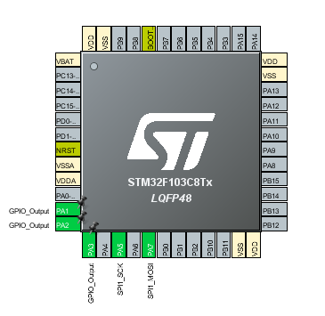
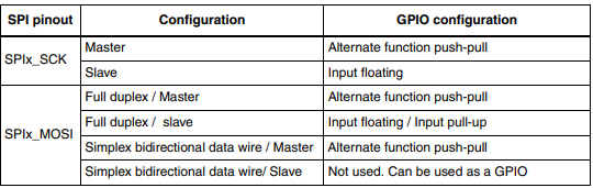
Connection
We will connect the display to the microcontroller via the SPI1 interface as follows:
- VDD-> + 3.3V
- GND-> Ground
- SCK -> PA5
- SDA -> PA7 (MOSI)
- RES-> PA1
- CS-> PA2
- DS-> PA3
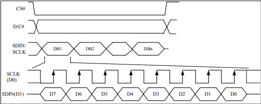
Data transmission occurs on the rising edge of the synchronization signal at 1 byte per frame. The SCK and SDA lines are used to transfer data via the SPI interface, RES - reboots the display controller at a low logic level, CS is responsible for selecting a device on the SPI bus at a low logic level, DS determines the type of data (command - 1 / data - 0) that are transmitted display. Since nothing can be read from the display, we will not use the MISO output.
Display Controller Memory Organization
Before displaying anything on the screen, you need to understand how the memory is organized in the ssd1306 controller.
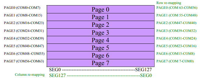
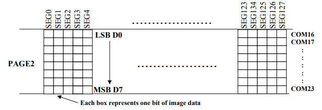
All graphics memory (GDDRAM) is an area of 128 * 64 = 8192 bits = 1KB. The area is divided into 8 pages, which are presented as a collection of 128 8-bit segments. Memory is addressed by page number and segment number, respectively.
With this method of addressing, there is a very unpleasant feature - the impossibility of writing 1 bit of information into memory, since the recording occurs in a segment (8 bits each). And since for the correct display of a single pixel on the screen, you need to know the state of the remaining pixels in the segment, it is advisable to create a 1 KB buffer in the microcontroller's memory and cyclically load it into the display memory (this is where DMA comes in handy), respectively, making its complete update. When using this method, it is possible to recalculate the position of each bit in memory to the classical coordinates x, y. Then, to display a point with coordinates x and y, we will use the following method:
displayBuff[x+(y/8)*SSD1306_WIDTH]|=(1<<(y%8));And in order to erase the point
displayBuff[x+(y/8)*SSD1306_WIDTH]&=~(1<<(y%8));SPI setup
As mentioned above, we will connect the display to SPI1 of the STM32F103C8 microcontroller.
For the convenience of writing code, we will declare some constants and create a function to initialize the SPI.
#define SSD1306_WIDTH 128
#define SSD1306_HEIGHT 64
#define BUFFER_SIZE 1024
//     ,     /
#define CS_SET GPIOA->BSRR|=GPIO_BSRR_BS2
#define CS_RES GPIOA->BSRR|=GPIO_BSRR_BR2
#define RESET_SET GPIOA->BSRR|=GPIO_BSRR_BS1
#define RESET_RES GPIOA->BSRR|=GPIO_BSRR_BR1
#define DATA GPIOA->BSRR|=GPIO_BSRR_BS3
#define COMMAND GPIOA->BSRR|=GPIO_BSRR_BR3

void spi1Init()
{
    return;
}
Turn on clocking and configure the GPIO outputs, as shown in the table above.
RCC->APB2ENR|=RCC_APB2ENR_SPI1EN | RCC_APB2ENR_IOPAEN;//  SPI1  GPIOA
RCC->AHBENR|=RCC_AHBENR_DMA1EN;//  DMA
GPIOA->CRL|= GPIO_CRL_MODE5 | GPIO_CRL_MODE7;//PA4,PA5,PA7    50MHz
GPIOA->CRL&= ~(GPIO_CRL_CNF5 | GPIO_CRL_CNF7);
GPIOA->CRL|=  GPIO_CRL_CNF5_1 | GPIO_CRL_CNF7_1;//PA5,PA7 -     push-pull, PA4 -  push-pull
Next, let's configure SPI to master mode and a frequency of 18 MHz.
SPI1->CR1|=SPI_CR1_MSTR;//
SPI1->CR1|= (0x00 & SPI_CR1_BR);//   2
SPI1->CR1|=SPI_CR1_SSM;// NSS
SPI1->CR1|=SPI_CR1_SSI;//NSS - high
SPI1->CR2|=SPI_CR2_TXDMAEN;//  DMA
SPI1->CR1|=SPI_CR1_SPE;// SPI1
Let's set up DMA.
DMA1_Channel3->CCR|=DMA_CCR1_PSIZE_0;//  1
DMA1_Channel3->CCR|=DMA_CCR1_DIR;// DMA
DMA1_Channel3->CCR|=DMA_CCR1_MINC;//
DMA1_Channel3->CCR|=DMA_CCR1_PL;//  DMA
Next, we will write a function for sending data via SPI (so far without DMA). The data exchange process is as follows:
- Waiting for SPI to be released
- CS = 0
- Sending data
- CS = 1
void spiTransmit(uint8_t data)
{
	CS_RES;
	SPI1->DR = data;
	while((SPI1->SR & SPI_SR_BSY))
	{};
	CS_SET;
}
We will also write a function for directly sending a command to the screen (We switch the DC line only when transmitting a command, and then return it to the “data” state, since we will not transmit commands so often and will not lose performance).
void ssd1306SendCommand(uint8_t command)
{
	COMMAND;
	spiTransmit(command);
	DATA;
}
Next, we will deal with functions for working directly with DMA, for this we will declare a buffer in the microcontroller memory and create functions for starting and stopping the cyclic sending of this buffer to the screen memory.
static uint8_t displayBuff[BUFFER_SIZE];//

void ssd1306RunDisplayUPD()
{
	DATA;
	DMA1_Channel3->CCR&=~(DMA_CCR1_EN);// DMA
	DMA1_Channel3->CPAR=(uint32_t)(&SPI1->DR);//  DMA    SPI1
	DMA1_Channel3->CMAR=(uint32_t)&displayBuff;//
	DMA1_Channel3->CNDTR=sizeof(displayBuff);//
	DMA1->IFCR&=~(DMA_IFCR_CGIF3);
	CS_RES;//
	DMA1_Channel3->CCR|=DMA_CCR1_CIRC;//  DMA
	DMA1_Channel3->CCR|=DMA_CCR1_EN;// DMA
}

void ssd1306StopDispayUPD()
{
	CS_SET;//
	DMA1_Channel3->CCR&=~(DMA_CCR1_EN);// DMA
	DMA1_Channel3->CCR&=~DMA_CCR1_CIRC;//
}
Screen initialization and data output
Now let's create a function to initialize the screen itself.
void ssd1306Init()
{

}
First, let's set up CS, RESET and DC line, and also reset the display controller.
uint16_t i;
GPIOA->CRL|= GPIO_CRL_MODE2 |GPIO_CRL_MODE1 | GPIO_CRL_MODE3;
GPIOA->CRL&= ~(GPIO_CRL_CNF1 | GPIO_CRL_CNF2 | GPIO_CRL_CNF3);//PA1,PA2,PA3
//
RESET_RES;
for(i=0;i<BUFFER_SIZE;i++)
{
	displayBuff[i]=0;
}
RESET_SET;
CS_SET;//
Next, we will send a sequence of commands for initialization (You can learn more about them in the documentation for the ssd1306 controller).
ssd1306SendCommand(0xAE); //display off
ssd1306SendCommand(0xD5); //Set Memory Addressing Mode
ssd1306SendCommand(0x80); //00,Horizontal Addressing Mode;01,Vertical
ssd1306SendCommand(0xA8); //Set Page Start Address for Page Addressing
ssd1306SendCommand(0x3F); //Set COM Output Scan Direction
ssd1306SendCommand(0xD3); //set low column address
ssd1306SendCommand(0x00); //set high column address
ssd1306SendCommand(0x40); //set start line address
ssd1306SendCommand(0x8D); //set contrast control register
ssd1306SendCommand(0x14);
ssd1306SendCommand(0x20); //set segment re-map 0 to 127
ssd1306SendCommand(0x00); //set normal display
ssd1306SendCommand(0xA1); //set multiplex ratio(1 to 64)
ssd1306SendCommand(0xC8); //
ssd1306SendCommand(0xDA); //0xa4,Output follows RAM
ssd1306SendCommand(0x12); //set display offset
ssd1306SendCommand(0x81); //not offset
ssd1306SendCommand(0x8F); //set display clock divide ratio/oscillator frequency
ssd1306SendCommand(0xD9); //set divide ratio
ssd1306SendCommand(0xF1); //set pre-charge period
ssd1306SendCommand(0xDB);
ssd1306SendCommand(0x40); //set com pins hardware configuration
ssd1306SendCommand(0xA4);
ssd1306SendCommand(0xA6); //set vcomh
ssd1306SendCommand(0xAF); //0x20,0.77xVcc
Let's create functions to fill the entire screen with the selected color and display one pixel.
typedef enum COLOR
{
	BLACK,
	WHITE
}COLOR;

void ssd1306DrawPixel(uint16_t x, uint16_t y,COLOR color){
	if(x<SSD1306_WIDTH && y <SSD1306_HEIGHT && x>=0 && y>=0)
	{
		if(color==WHITE)
		{
			displayBuff[x+(y/8)*SSD1306_WIDTH]|=(1<<(y%8));
		}
		else if(color==BLACK)
		{
			displayBuff[x+(y/8)*SSD1306_WIDTH]&=~(1<<(y%8));
		}
	}
}

void ssd1306FillDisplay(COLOR color)
{
	uint16_t i;
	for(i=0;i<SSD1306_HEIGHT*SSD1306_WIDTH;i++)
	{
		if(color==WHITE)
			displayBuff[i]=0xFF;
		else if(color==BLACK)
			displayBuff[i]=0;
	}
}
Next, in the body of the main program, we initialize the SPI and the display.
RccClockInit();
spi1Init();
ssd1306Init();
The RccClockInit () function is intended for setting the microcontroller clock.
RccClockInit code
int RccClockInit()
{
	//Enable HSE
	//Setting PLL
	//Enable PLL
	//Setting count wait cycles of FLASH
	//Setting AHB1,AHB2 prescaler
	//Switch to PLL
	uint16_t timeDelay;
	RCC->CR|=RCC_CR_HSEON;//Enable HSE
	for(timeDelay=0;;timeDelay++)
	{
		if(RCC->CR&RCC_CR_HSERDY) break;
		if(timeDelay>0x1000)
		{
			RCC->CR&=~RCC_CR_HSEON;
			return 1;
		}
	}
	RCC->CFGR|=RCC_CFGR_PLLMULL9;//PLL x9
	RCC->CFGR|=RCC_CFGR_PLLSRC_HSE;//PLL sourse:HSE
	RCC->CR|=RCC_CR_PLLON;//Enable PLL
	for(timeDelay=0;;timeDelay++)
	{
		if(RCC->CR&RCC_CR_PLLRDY) break;
		if(timeDelay>0x1000)
		{
			RCC->CR&=~RCC_CR_HSEON;
			RCC->CR&=~RCC_CR_PLLON;
			return 2;
		}
	}
	FLASH->ACR|=FLASH_ACR_LATENCY_2;
	RCC->CFGR|=RCC_CFGR_PPRE1_DIV2;//APB1 prescaler=2
	RCC->CFGR|=RCC_CFGR_SW_PLL;//Switch to PLL
	while((RCC->CFGR&RCC_CFGR_SWS)!=(0x02<<2)){}
	RCC->CR&=~RCC_CR_HSION;//Disable HSI
	return 0;
}
Fill the entire display with white and see the result.
ssd1306RunDisplayUPD();
ssd1306FillDisplay(WHITE);

Let's draw on the screen in a grid in 10 pixel increments.
for(i=0;i<SSD1306_WIDTH;i++)
{
	for(j=0;j<SSD1306_HEIGHT;j++)
	{
		if(j%10==0 || i%10==0)
			ssd1306DrawPixel(i,j,WHITE);
	}
}
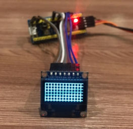
The functions work correctly, the buffer is continuously written to the memory of the display controller, which allows using the Cartesian coordinate system when displaying graphic primitives.
Display refresh rate
Since the buffer is sent cyclically to the display memory, it will be enough to know the time it takes for the DMA to complete the data transfer to estimate the display refresh rate. For real-time debugging, we'll use Keil's EventRecorder library.
In order to find out the moment of the end of the data transfer, we will configure the DMA interrupt at the end of the transfer.
DMA1_Channel3->CCR|=DMA_CCR1_TCIE;//
DMA1->IFCR&=~DMA_IFCR_CTCIF3;//
NVIC_EnableIRQ(DMA1_Channel3_IRQn);//
We will track the time interval using the EventStart and EventStop functions.

We get 0.00400881-0.00377114 = 0.00012767 sec, which corresponds to a refresh rate of 4.2 KHz. In fact, the frequency is not so high, which is due to the inaccuracy of the measurement method, but clearly more than the standard 60 Hz.