Buck's invention survived the creator. Moreover, it is alive to this day: the cryotron is at the heart of IBM's projects to create superconducting qubits.
Nevertheless, decades of work on the cryotron were lost in the pages of the history of computer engineering. Many modern engineers have never even heard of this technology. Let's talk about Buck's work and his now-forgotten cryotronic computer.
After World War II, electronics engineers were faced with a fundamental question: how should electronic digital computers be built? What type of switches is best for logic circuits? What to use for main memory?
Without thinking twice, from a variety of options, they chose vacuum tubes to use as the main logic switch. Moreover, to build just one car, thousands of these lamps were required. Nobody seriously considered transistors then - they had just been developed by Bell Telephone Laboratories.
There were also plenty of options for "memory": special cathode-ray and mercury tubes, rotating magnetic drums. By the 1950s, another promising candidate emerged: magnetic cores. One ring, made of ferromagnet, could contain 1 bit of data, depending on which direction it was magnetized in.
In the mid-50s, the world of the first computers was populated by lamp mainframes with magnetic core memory. As you know, after some time, lamps were replaced by transistors, and then - integrated circuits, both for the implementation of logic and for memory. But in the 1950s-1960s. various groups of engineers were looking for fundamentally new ways to create digital computers.
One of the most notable "radical" scientists was Dudley Allen Buck. He worked at MIT from 1950 to 1959 - until his tragic death at the age of 32. He made important contributions to early research in the field of chip design. In addition, he is responsible for the development of the cryotron, a superconducting switch. According to Buck, his brainchild was supposed to be the main building block for all digital computers of the future. He was trusted by the giants: GE, IBM, RCA and the US military. In the late 1950s, large research projects were launched on the cryotron. They ended only after the industry had unambiguously chosen the "successor to the lamps" - silicon microchips.

Handmade: Buck has created many prototypes, including a circuit diagram of a multivibrator [close-up, top], which consists of 19 individual cryotrons [bottom].
In 1948, Dudley Buck received his BS in Electrical Engineering from the University of Washington. His first job was the cryptology organization of the US Navy. There he met the first digital computers. In 1950, he joined the Massachusetts Institute of Technology and entered graduate school in electrical engineering with the physicist Arthur von Hippel. Baku had a chance to take part in the Whirlwind project of the Massachusetts Institute of Technology, a technological monster designed for military purposes.
Jay Last, Buck's graduate student at MIT, who later led the team behind Fairchild Semiconductor's first planar silicon integrated circuit, recalls him as "a great visionary" and "a good man ... an obscenely good man." Confirmation of Last's impression can be found in a letter Buck wrote in 1954, when he was only 27 years old:
“I have an adopted son. Of his 17 years, 4 he lived with me. I was a scoutmaster for 6 years and now I go to a Methodist church. Sometimes on Sundays I even get up in the pulpit. I love working with both human and engineering values equally. "
Despite his rich social and personal life, Buck continued to work at MIT with great dedication. In the Whirlwind project, he selected materials for the manufacture of magnetic cores. In addition, he was in constant search of materials that could be used as a basis for new generation switches.
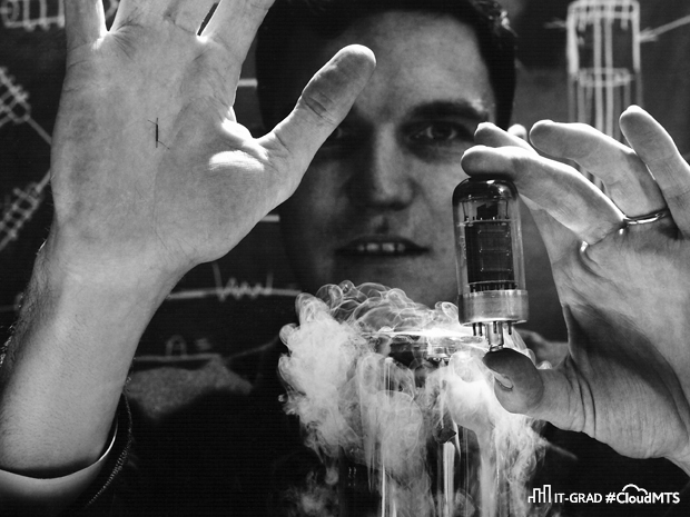
And in 1952, Buck's attention was drawn to the chemical element bismuth, known for its strong magnetic resistance: its electrical resistivity rises sharply in response to a magnetic field, especially at low temperatures. At the boiling point of liquid helium (4.2 kelvin), the electrical resistance of bismuth changes tens of millions of times when a strong magnetic field is applied. This behavior could be useful for building computers, Buck thought. The relatively small current in the test wire and the magnetic field it creates can cause a huge change in the resistivity of bismuth, suddenly inhibiting or allowing current to pass through it. It will be a real electronic switch!
By 1954 Buck had noticed an even more interesting property of electromagnetism, discovered at low temperatures of liquid helium: superconductivity. This phenomenon, although peculiar, has already been studied earlier. Since the beginning of the 20th century, physicists have known that when cooled to temperatures close to the boiling point of liquid helium, various metals completely lose their electrical resistance.
Superconductivity also has a magnetic aspect known as the Meissner effect. Superconducting material is not affected by magnetic fields - but only up to a certain point. If a sufficiently strong magnetic field is applied, the material almost instantly becomes resistive. If the magnetic field is removed, the material returns to a superconducting state.
Buck saw the potential of this phenomenon for electronic digital computers: a magnetically controlled superconducting switch could be created. This invention could fit both lamps and magnetic cores onto blades! A superconducting switch can be very compact, fast and energy efficient.
In the spirit of 1950s futurism, the tank called his invention a cryotron - a mixture of the words cryo (ϰρύος, Greek for "icy cold, frost") and electronics. But coming up with technology and giving it a name was not enough. Buck immediately began building and testing dozens of prototypes.
Buck's first cryotrons were ridiculously simple. They consisted of a piece of tantalum wire in a tight copper winding. Electrical leads were connected to the ends of the copper and tantalum wires, and the cryotron was immersed in a container with liquid helium.
A current flowed through the copper winding, which created a magnetic field. Buck could make tantalum wire both superconducting and restore resistance to it. The prototypes turned out to be working. The very small current in the winding made it possible to control a much higher current in the tantalum wire. Baka's cryotron functioned as a logic switch of a digital computer, no worse than lamps and transistors.
Buck was captured by the prospect of a new device. In his master's thesis, he envisioned the creation of entire arrays of cryotrons. Buck believed that even from his simple prototypes, a digital computer could be built, where cryotrons would be used for both logic and memory. However, there was one problem: the switching speed of the cryotron was only slightly higher than that of an electromechanical relay.
In search of the best, Buck tried a wide variety of different materials. The combination of a lead winding with niobium, for example, gave a switching time of 5 microseconds. Not bad, but still much slower than the fastest transistors of the time - they switched 100 times faster. According to Buck, by reducing the physical size of the cryotron, it was possible to achieve performance no lower than that of the fastest transistors.
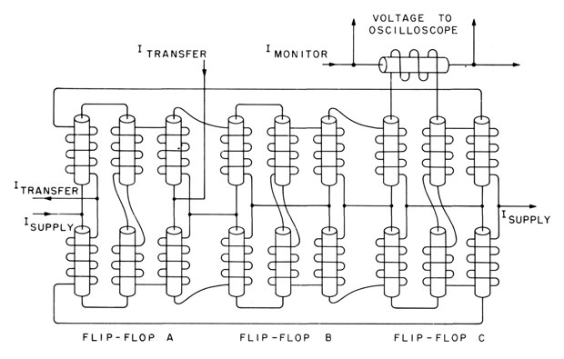
By piecing together several prototypes of the cryotron, Buck successfully fabricated a logic gate, flip-flop, and amplifier with a splitter. It turns out that with the help of cryotrons alone, it is possible to assemble all the basic circuits for digital computer memory and logic. The cryotronic superconducting computer is no longer an idyllic dream.
Whirlwind: Buck hoped that one day engineers would be able to fit a computer of the same power into a breadbox-sized
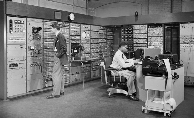
case. Buck's research program expanded at this stage. He believed that, using microminiaturization techniques, he could create a computer containing tens of thousands of cryotrons. Buck's machine will have the processing power of the Whirlwind, one of the most advanced digital computers in the world. But Whirlwind occupied several rooms and consumed 150 kilowatts of electricity.
The 28-year-old engineer essentially proposed shrinking Whirlwind to the size of a radio, submerging it in a bath of liquid helium, and running it. According to him, a computer will consume as much as an ordinary light bulb on a Christmas tree. This is a bold statement, but the young scientist's enthusiasm and strong reasoning convinced his colleagues to give his project the green light.
Cryotron research was officially assigned to Buck at the Lincoln Laboratory at MIT. While continuing to work on compact, faster and more energy efficient cryotrons, he simultaneously began a project to create a "large" computer memory, for which the low switching speed of existing cryotrons would not matter.
For content-addressable memory (later name), Buck proposed a circuit of 75,000 cryotrons. Buck himself called it the recognition unit, since each memory cell was checked for the presence of the desired information.
This kind of memory has been useful for cryptanalysis where pattern identification is important. A fully assembled cryotronic recognition unit was supposed to be no larger than a portfolio and at the same time have a memory capacity comparable to Whirlwind - 3.2 kilobytes.
When Buck was preparing a patent application for a cryotron in mid-1955, rumors of his work to create content-addressable memory leaked into cryptology and computing circles in the United States, causing a stir. In July of that year, John McPherson, IBM's vice president and a leading e-computing specialist, wrote to Baku that William Friedman, the NSA's chief cryptologist, was "very interested" in the superconducting components of Buck's computer. Just a few days later, the Cryotron (Magnetically Controlled Gating Element) was patented. The application contained a wide list of the cryotron's capabilities and options for using it in computers.
By this time, Buck's research on the cryotron had gone beyond the MIT. He signed a consulting agreement on cryotron technology with research firm Arthur D. Little. The company was a stone's throw from the MIT campus and was a leading manufacturer of cryostats for the production of liquid helium in the 1950s. With NSA sponsorship, Buck and staff at AD Little began developing cryotronic memory. Their first project together was a small proof-of-concept memory.
In 1955, Buck focused on creating miniature cryotrons and integrated matrices using thin sprayed films. Instead of winding small wires on top of each other, he wanted to vaporize the metal through a stencil-like "mask" onto a substrate and create a subtle pattern of superconducting material. A second, controlling layer was sprayed on top of this film. It was necessary to "print" entire arrays of cryotrons.
During the preparation, Buck tested many materials: alloys of lead, bismuth, strontium, indium and other elements. As a result, he managed to create a 100 nanometer thick lead-bismuth-strontium alloy film. It could switch between superconducting and resistive states in 0.1 microseconds, which was ten times less than the speed of the fastest transistor at the time. In addition, Buck developed many binary circuits that could be built exclusively from cryotrons - triggers, valves, multivibrators, adders, and batteries.
After registering a patent and completing research, Buck was ready to announce the cryotron to the world. In November 1955, he submitted a paper entitled "Cryotron - Superconducting Computer Component" to the Institute of Radio Engineers, one of the predecessor organizations of the IEEE. In the article, Buck detailed a wire-wound cryotron and a number of basic digital circuits that can be assembled using it, highlighting the importance of this superconducting device in computing. "The cryotron in its current state ... can be used as an active element in logic circuits," Buck wrote. He could not resist the bold statement that in the near future "a large digital computer will take only one cubic foot ... and half a watt of power will be enough for it."
On the contrary, Buck wrote very modestly about the speeds of cryotrons: “At present, the device works somewhat faster than electromechanical relays, but much slower than vacuum tubes and transistors. We are working to increase the speed. " Although thin-film cryotrons comparable to transistors have already been tested, Buck has been slow to share this information with the public.

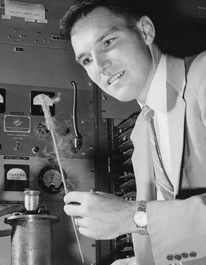
Let's compare the dimensions: The tank holds a prototype cryotron, an electric vacuum tube and a transistor in the palm of its hand.
By the time the article was published in Proceedings of the IRE (April 1956), thin-film cryotrons were already undergoing tests. Under Buck's direction, NSA engineer Albert Slade began his own research on cryotronic circuits.
Around the same time, Buck presented von Hippel with a topic for his doctoral dissertation - the study of thin films of superconducting materials and how to control their thickness and geometry to create fast switching cryotrons. Von Hippel approved of the topic and called it extremely promising.
Until his death in 1959Buck was actively involved in the development of integrated cryotronic microcircuits. Albert Slade transferred from NSA to Arthur D. Little specifically to work on cryotronic memory. Another NSA specialist, Horace Tharp Mann, with Buck's support, began studying thin-film cryotrons. In 1957, IBM and RCA launched their own NSA-funded programs to develop a high-speed thin-film cryotron. GE also did not stand aside, starting internal research. Buck, still an MIT graduate student, faced fierce competition for the first time.
In his usual manner, Buck decided to set himself an even higher goal. He recruited Kenneth R. Shoulders of the von Hippel laboratory to work. Shoulders at that time was engaged in another innovative technology: the use of electron beams for "micromachinery", etching of extremely small microcircuits. This technology, later called electron beam lithography, was used to create silicon microchips. In the mid-1950s, Shoulders tried to create an electronic device smaller than 100 nm - even smaller than a virus or anything that humans have ever done. Shoulders' ambitions matched perfectly with Buck's desire to increase the speed of cryotrons through miniaturization and create large-scale integrated arrays from them.
They worked together until mid-1958. Buck earned his Ph.D. and an assistant professor in the Department of Electrical Engineering at MIT, and Shoulders moved to Stanford Research Institute in Menlo Park.
Summing up their collaboration, Buck and Shoulders presented a paper titled "An Approach to Microminiature Printing Systems." “The day is approaching when digital computers will no longer be manufactured by assembling thousands of custom-made parts,” they wrote. "Instead, the entire computer, or a very large portion of it, is likely to be manufactured at one time."
Just five months after the presentation of the report, Buck passed away suddenly. The last entry in his laboratory notebook, dated May 18, 1959, describes his attempt to create a boron sputter. On May 21, Buck died of respiratory failure - he had just turned 32.
Contemporaries were inclined to believe that the cause of death was viral pneumonia. However, it is likely that his experiments with spraying are to blame. It was on May 18 that he worked with elements that required special care. He used gaseous boron trichloride as the boron source. During the deposition of the film, gaseous hydrogen chloride was formed. Exposure to any gas, let alone a mixture of several, can cause pulmonary edema with symptoms similar to pneumonia. Aside from the general university curriculum, Buck was not a professional chemist and may not have realized the danger. Or he simply did not have sufficient bench experience to handle these gases safely. One way or another, for colleagues, Buck's death was a tragedy.

Excerpt from Buck's 1956 report.
Research on the cryotron did not end with Buck's death. Active work continued until the 1960s. Mann, who worked on thin-film cryotrons at the NSA, took a job at TRW's space technology laboratory in Los Angeles. There, until 1966, he was engaged in electron-beam lithography to create thin-film cryotrons. AD Little employees also continued to develop cryotronic memory in an attempt to implement Buck's idea.
GE, IBM and RCA developed thin-film cryotron microcircuits in the early 1960s, in particular for memory. By 1961, GE researchers had built a working integrated shift register out of thin-film cryotrons. In complexity, it was not inferior to the silicon integrated circuits of the time. And two years later, the GE cryotronic chip surpassedsilicon microchips by the level of integration. Scientists have even made an experimental working computer from three arrays of integrated cryotrons.
Despite all this research, the rapid development of silicon microchips - in particular, their cost reduction - in the 1960s overshadowed the progress in the study of cryotrons. New computers were built on silicon logic circuits with magnetic core memory. By the mid-1960s, most cryotron researchers had finally turned their attention to silicon.
Nevertheless, someone remained loyal to the cryotron. Of particular interest to scientists were cryotrons, in which a quantum mechanical phenomenon called the Josephson effect was observed. In the early 1970s, IBM researchers created modified cryotrons known as Josephson junctions. Research on them continued until the 1980s. And Josephson junctions are still the cornerstone of modern quantum computing research at IBM and other companies.
The cryotron has not disappeared anywhere. He still lives - in different guises and under different names - in the long shadow of a silicon microchip. And who knows what Buck would have accomplished had he lived longer.
, , , . , . . , , — .
, Amazon Braket Rigetti Computing, IonQ D-Wave Systems. Microsoft Azure Quantum, , . IBM Quantum Experience, , IBM .