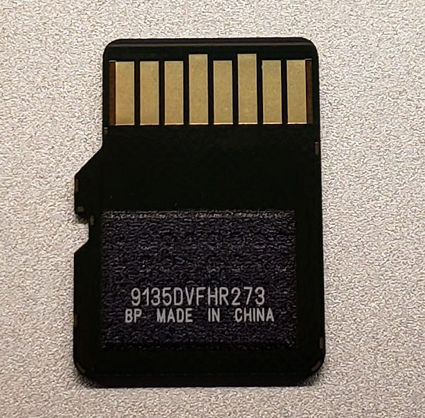
Previously, I looked at SanDisk microSD cards for use in write-intensive applications such as dash cameras. Then I studied the results of the speed tests and thought about what type of NAND Flash is used in the card. SanDisk does not publish detailed descriptions of the internals of the cards, so I had no choice but to reverse-engineer the card myself.
Technical support that failed
Hoping to dig up information, I sent an email to SanDisk support asking what type of NAND Flash they use in their High Endurance line, as well as endurance metrics such as P / E (Program / Erase) cycles, and total the number of terabytes written (TBW). Unfortunately, the SanDisk support staff was unable to provide satisfactory answers to my questions as they do not provide information not covered by the published specifications. I was told that all of their cards use MLC Flash, which is correct if you call TLC Flash 3-bit "MLC" (as Samsung does).
Dear Jason,
Thank you for contacting SanDisk Global Customer Support. We appreciate you being a member of our SanDisk family.
I understand you want to know more about our SanDisk High Endurance video monitoring card. Let us inform you that all of our memory cards use Multi level cell flash technology . However, the number of flash memory read / write cycles is not published or documented. Only read and write speeds are published, namely 100 MB / s and 40 MB / s. The 64GB card can record Full HD video for up to 10,000 hours. Details can be found here.
SANDISK HIGH ENDURANCE VIDEO MONITORING microSD CARD
Regards, ...
I'll give them a medal with the words "you tried".
Anatomy of an SD card
The microSD card may seem like a monolithic device. However, these cards are made up of many different chips, each of which plays a role. The simplest SD card will have a controller that controls the NAND Flash chips and communicates with the host (PC, camera, etc.), as well as with the NAND Flash itself (consisting of one or more flash crystals). The Bunnie Studios blog has an excellent article on the construction of SD cards, including descriptions of counterfeits and their manufacture.
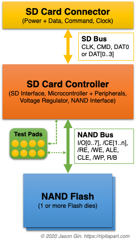
Block Diagram of a Typical SD Card
MicroSD cards are often (but not always) found test sites used for programming and testing NAND Flash in production. They can be used to recover data, or reusing microSD cards with a defective controller or firmware. They allow you to turn a card into a simple NAND Flash - you can read about this on the blog of Gao Louis. Note that there is no standard for such test sites (even within one manufacturer), however, some manufacturers, in particular SanDisk, have patterns that facilitate reverse engineering.
Crouching Controller, Lurking Test Pads
MicroSD cards fall into the category of “monolithic” flash devices because they combine a controller and NAND Flash into a single, non-separable package. Many manufacturers are bringing the flash data bus to hidden (and virtually no documentation) test sites. With their help, other manufacturers of memory cards and USB flash drives make inexpensive drives from failed parts. The controller can simply be turned off, and the flash can be used like a normal chip.
In the case of SanDisk cards, pinout information for their test pads is extremely scarce. Each generation has its own differences, but the layout remains largely unchanged. The differences can be fatal, since the pins for power and ground are sometimes swapped (and if the polarity is incorrect, the chip will die instantly!).
My card (as well as many of the company's cards from an expensive line - not Ultra) have test pads covered not with varnish, but with some kind of screen-printed epoxy with a laser cut serial number. I warmed it up, scraped it, and managed to remove this very fragile coating from the test pads. In doing so, I also removed the serial number - this is probably something like a warranty seal.
Epoxy Test Pads
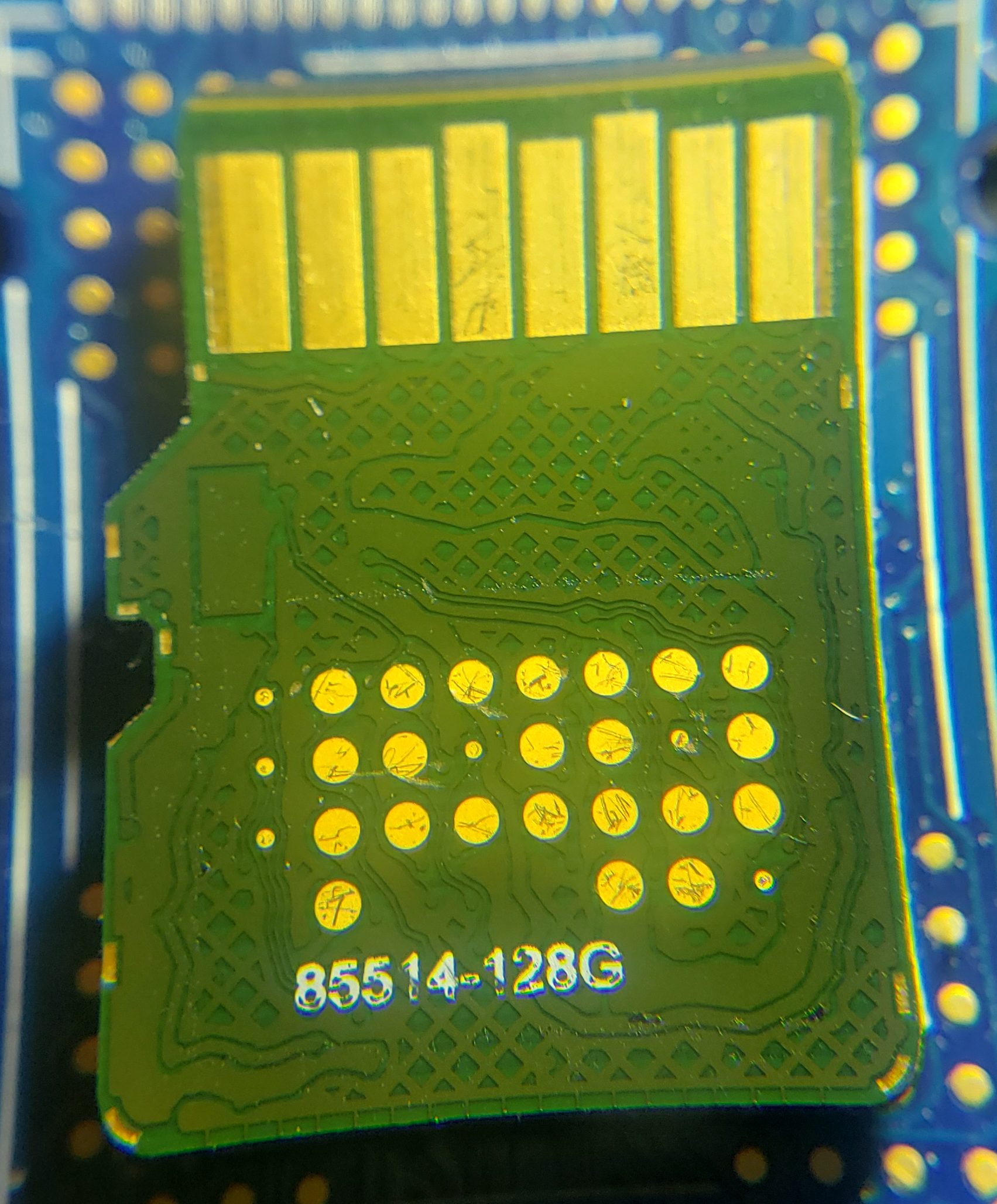
Outline Test
Pads After removing traces of epoxy coating, I came across a familiar layout of test pads, to which a few additional ones were added below.
Creating an interface module
The interface module concept is pretty simple. For each of the test pads, we pull out a wire leading to a larger pad for easier access, and connect the normal SD bus to the SD connector so that the controller does its job while we tinker with the NAND Flash bus. Considering the small size of the test sites and their large number, the result may turn out to be a little sloppy.
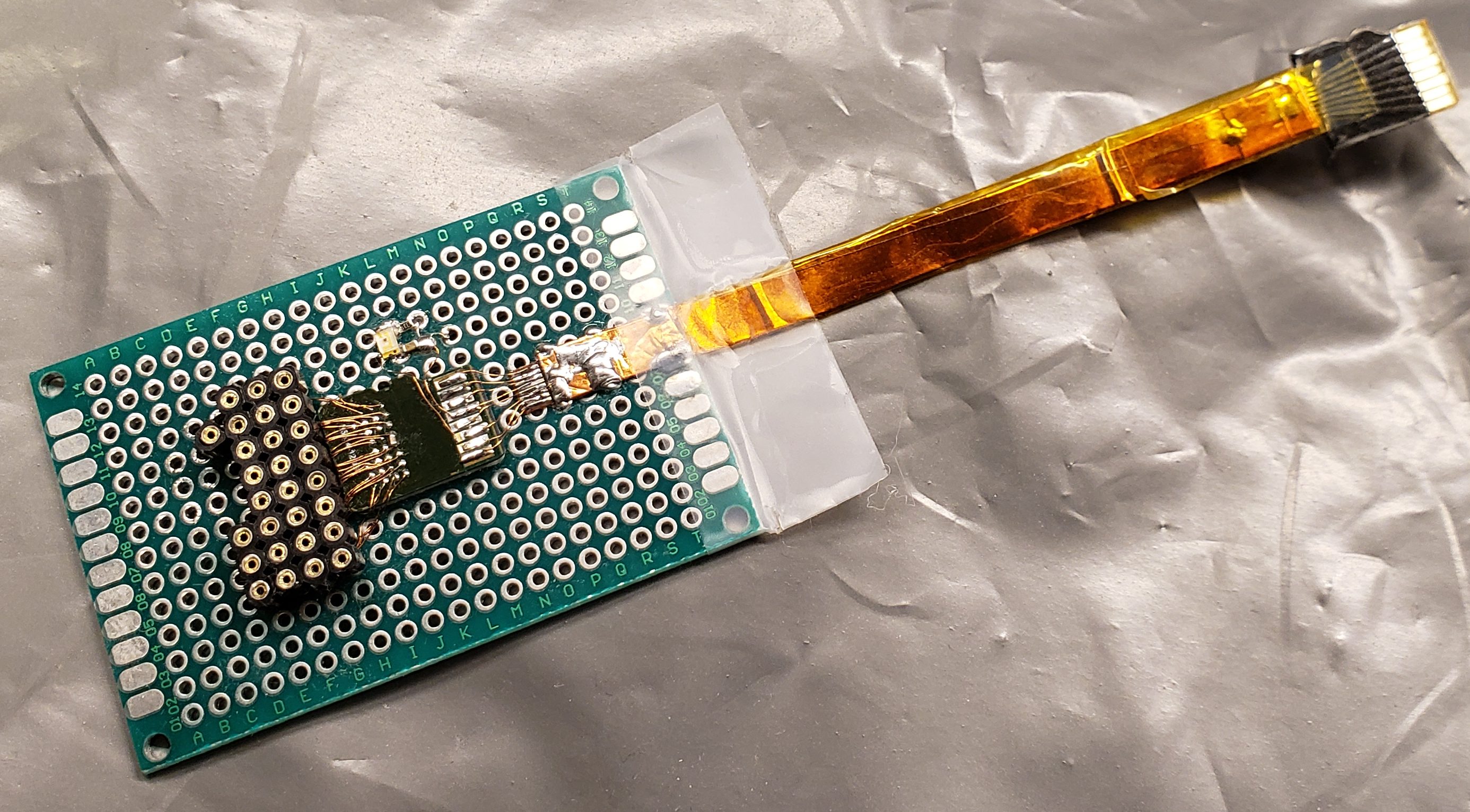
Interface module assembly

Interface module, enlarged photo
I started by affixing the card with double-sided tape to the breadboard. Then I tinned all the pads and soldered a small 1uF ceramic capacitor to the Vcc and GND pads of the card. Using 40 AWG (0.1mm) enamelled wire, I connected each test pad to the corresponding pin on the breadboard. Together with the additional sites, this amounted to 28 tiny wires!
For the SD connector I used a cable with a device for servicing Android phones from HTC " XTC 2 ClipIt worked like a 'flexible remote SD card' and routed the signals through a small flex cable. I wrapped the cable with copper tape to protect it from noise and amplification, and soldered the tape to the outer pads of the breadboard to strengthen the structure. Then I tinned the end of the cable, and connected the enamelled wires to the pins of the card, then I inserted an LED with a resistor into the power wire so that I could see when the card was powered.
Bus analysis
Having spread all the test sites for test contacts, I could begin to understand what these contacts are responsible for in terms of access to the NAND Flash located inside the card.

In general, the pin layout was the same as most SanDisk microSD cards.
To analyze the signals from all pins, I used a DSLogic Plus logic analyzer... The pinout for data transfer was already known, and the hardest work had already been done (data bus, control, addresses, commands, write protection, busy / free status). However, the role of not each of the contacts was immediately obvious - the pinout I found included the minimum number of buses that allowed working with NAND Flash - with the exception of the control bus, which puts the controller into reset mode and disconnects it from data bus control (this will be important later) ...
By listening to the data bus at the maximum speed available to DSLogic (and using the available 32 MB buffer), I was able to compile a clear list of commands sent to the NAND Flash from the controller at the time of initialization.
Basics of bus listening and NAND I / O (writing commands, addresses, reading data)
I specifically looked for two commands: RESET (0xFF) and READ ID (0x90). When looking for command sequences, it is important to know when and how the data and control buses change. I will try to explain everything step by step. If you are interested, I recommend Micron's manual , which describes the basics of NAND Flash and gives much more information about the principles of its operation.
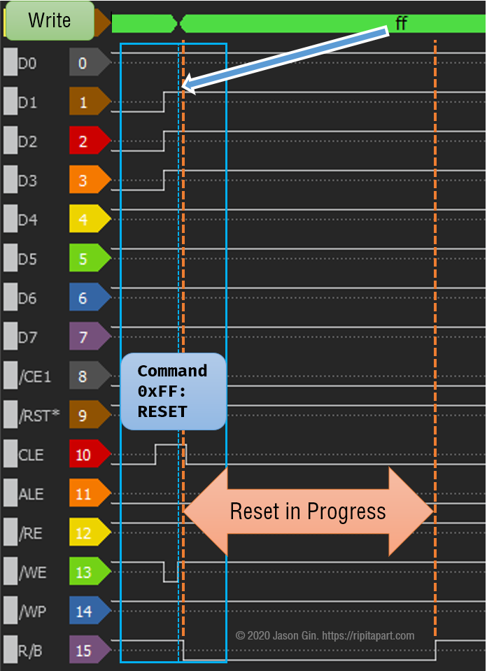
SanDisk High Endurance 128GB RESET Command Tracking with Logic Analyzer. The dotted line marks the appearance of the write and reset commands.
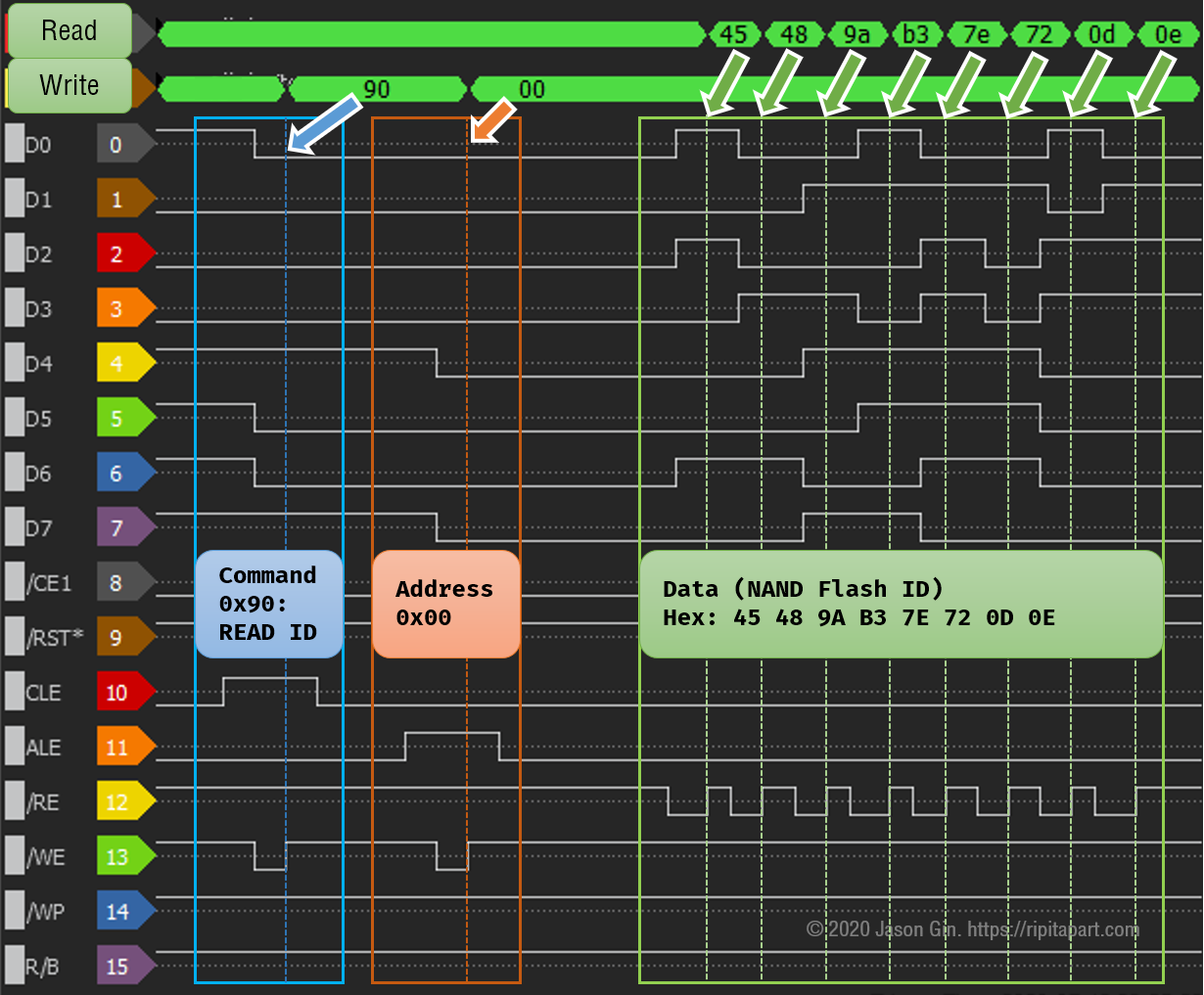
SanDisk High Endurance 128GB RESET Command Tracking with Logic Analyzer. The dotted line marks the appearance of read / write commands.
When the RESET command is sent to the NAND Flash, the / CE (Chip Select, Active Low) bus is pulled down first. Then the CLE bus (Command Latch Enable) is pulled up; the data bus is set to its scheduled value 0xFF (in binary); then the / WE (Write Enable, Active Low) bus goes from high to low voltage, and then returns to high (data from the data bus is transferred to the chip when the / WE bus goes from low voltage to high, the so-called signal edge "); the CLE bus is pulled back downward, returning to normal. The flash chip then pulls the R / B (Ready / Busy Status) bus down to indicate that it is busy with a reset, and when finished, pulls the bus back up.
The READ ID command works in a similar way, except that after writing the command 0x90 (1001 0000) to the data bus, it pulls up the ALE (Address Latch Enable) bus, not CLE, and writes 0x00 (all binary zeros), resulting in / WE to the lower state. The chip transfers the NAND Flash ID written to it to the internal read register, and data is read from the device on each edge of the bus / RE (Read Enable, Active Low); for most devices this is 4 to 8 bytes of data.
NAND Flash ID
Each NAND Flash device has its own (for the most part) unique identifier that relates it to a specific manufacturer and other manufacturer-specific functional data. In other words, only the manufacturer ID assigned by the JEDEC technology association is well defined .
The first byte indicates the manufacturer of the chip, and the rest (from 2 to 6) define the characteristics of the device - all of them are determined by the manufacturer itself. Most NAND manufacturers are very reluctant to publish specifications for devices, and SanDisk (and thus Toshiba / Kioxia) is very tightly controlled by this data, with the exception of slightly outdated Toshiba datasheets leaked online. Since these companies share manufacturing capacity, an educated guess can be made that the data structures in manufacturer-defined data can be matched against each other.
As for the 128GB SanDisk High Endurance card, it uses NAND Flash ID of 0x45 48 9A B3 7E 72 0D 0E. Some of these figures can be compared to the Toshiba spec :
| Byte (hex) | |
|---|---|
| 45
|
: SanDisk
|
| 48
|
I/O : 1.8 volts ( )
: 128 ( ) |
| 9A
|
NAND: TLC (Triple-Level Cell / 3 )
/CE: 4 ( 4 32 ) |
| B3
|
: 12 (768 )
: 16 384 / 16 |
| 7E
|
/CE: 8 (2 )
|
| 72
|
:
: BiCS3 3D NAND |
| 0D
|
( )
|
| 0E
|
( )
|
Although not all byte values can be determined unambiguously, I was able to determine that SanDisk High Endurance cards use BiCS3 3D TLC NAND Flash - at least this is 3D NAND, which significantly exceeds traditional flat NAND in terms of reliability. Unfortunately, this information alone cannot tell whether the controller is taking advantage of the SLC caching mechanism in write operations.
The geometry of the manufacturing process of the chip is determined based on the first four bytes of Flash ID and their comparison with the line of the configuration file of tools from Silicon Motion for the SM3271 USB Flash controller and SM2258XT controllerDRAM-less SSD. These tools give alleged SKUs from SDTNAIAMA-256G and SDUNBIEMM-32G chips respectively, but it seems to me that this does not correspond to the flash memory configuration in this card.
External control
I wanted to make sure I was getting the correct ID from the NAND Flash, so I connected a Texas Instruments MSP430FR2433 debug board and wrote the simplest code that sends the necessary RESET and READ ID commands, and tries to extract additional data from the hidden parameters of the JEDEC Parameter Page in parallel.
The first obstacle I got in my way was that the MSP430 was reset every time I tried to send a RESET command, which indicated that the limited power supply of the MSP430 board could not cope with this current. This can happen when " bus contention"when two devices are fighting with each other, trying to simultaneously apply high and low voltage to a certain digital bus. I was not sure that I understood what was happening, since there is no free information on how to turn off the built-in card controller. was (and because of this he "releases" the NAND bus and allows another device to take control of it.)
I figured out that the A1 test pad (see diagram) is the controller's reset bus, and if you keep its voltage in the lower position, the controller completely frees control over the NAND Flash bus.After that my code from the microcontroller was able to read the Flash ID correctly and without hindrance.

Reading Flash ID from the card
The JEDEC Settings Page ... or at least what SanDisk has done with it!
If available, the JEDEC parameters page contains detailed characteristics of the Flash chip - much more detailed than the NAND Flash ID - and, moreover, more standardized. It turned out, however, that SanDisk chose to ignore the standard and use its own! Usually the page starts with the ASCII string "JEDEC", however I found a duplicate string "SNDK" ( company name on the exchange ) and other data that did not match anything from the JEDEC specification! Well, worth a try.
I collected data using the same Arduino sketch I showed earlier, and received 1536 bytes of data. On Ideone I wrote a little program to convert the first 512 bytes into a neat HEX dump:
Offset 00:01:02:03:04:05:06:07:08:09:0A:0B:0C:0D:0E:0F 0123456789ABCDEF


------ --+--+--+--+--+--+--+--+--+--+--+--+--+--+--+-- ----------------


0x0000 53 4E 44 4B 53 4E 44 4B 53 4E 44 4B 53 4E 44 4B SNDKSNDKSNDKSNDK


0x0010 53 4E 44 4B 53 4E 44 4B 53 4E 44 4B 53 4E 44 4B SNDKSNDKSNDKSNDK


0x0020 08 08 00 08 06 20 00 02 01 48 9A B3 00 05 08 41 ..... ...H.....A


0x0030 48 63 6A 08 08 00 08 06 20 00 02 01 48 9A B3 00 Hcj..... ...H...


0x0040 05 08 41 48 63 6A 08 08 00 08 06 20 00 02 01 48 ..AHcj..... ...H


0x0050 9A B3 00 05 08 41 48 63 6A 08 08 00 08 06 20 00 .....AHcj..... .


0x0060 02 01 48 9A B3 00 05 08 41 48 63 6A 08 08 00 08 ..H.....AHcj....


0x0070 06 20 00 02 01 48 9A B3 00 05 08 41 48 63 6A 08 . ...H.....AHcj.


0x0080 08 00 08 06 20 00 02 01 48 9A B3 00 05 08 41 48 .... ...H.....AH


0x0090 63 6A 08 08 00 08 06 20 00 02 01 48 9A B3 00 05 cj..... ...H....


0x00A0 08 41 48 63 6A 08 08 00 08 06 20 00 02 01 48 9A .AHcj..... ...H.


0x00B0 B3 00 05 08 41 48 63 6A 08 08 00 08 06 20 00 02 ....AHcj..... ..


0x00C0 01 48 9A B3 00 05 08 41 48 63 6A 08 08 00 08 06 .H.....AHcj.....


0x00D0 20 00 02 01 48 9A B3 00 05 08 41 48 63 6A 08 08 ...H.....AHcj..


0x00E0 00 08 06 20 00 02 01 48 9A B3 00 05 08 41 48 63 ... ...H.....AHc


0x00F0 6A 08 08 00 08 06 20 00 02 01 48 9A B3 00 05 08 j..... ...H.....


0x0100 41 48 63 6A 08 08 00 08 06 20 00 02 01 48 9A B3 AHcj..... ...H..


0x0110 00 05 08 41 48 63 6A 08 08 00 08 06 20 00 02 01 ...AHcj..... ...


0x0120 48 9A B3 00 05 08 41 48 63 6A 08 08 00 08 06 20 H.....AHcj.....


0x0130 00 02 01 48 9A B3 00 05 08 41 48 63 6A 08 08 00 ...H.....AHcj...


0x0140 08 06 20 00 02 01 48 9A B3 00 05 08 41 48 63 6A .. ...H.....AHcj


0x0150 08 08 00 08 06 20 00 02 01 48 9A B3 00 05 08 41 ..... ...H.....A


0x0160 48 63 6A 08 08 00 08 06 20 00 02 01 48 9A B3 00 Hcj..... ...H...


0x0170 05 08 41 48 63 6A 08 08 00 08 06 20 00 02 01 48 ..AHcj..... ...H


0x0180 9A B3 00 05 08 41 48 63 6A 08 08 00 08 06 20 00 .....AHcj..... .


0x0190 02 01 48 9A B3 00 05 08 41 48 63 6A 08 08 00 08 ..H.....AHcj....


0x01A0 06 20 00 02 01 48 9A B3 00 05 08 41 48 63 6A 08 . ...H.....AHcj.


0x01B0 08 00 08 06 20 00 02 01 48 9A B3 00 05 08 41 48 .... ...H.....AH


0x01C0 63 6A 08 08 00 08 06 20 00 02 01 48 9A B3 00 05 cj..... ...H....


0x01D0 08 41 48 63 6A 08 08 00 08 06 20 00 02 01 48 9A .AHcj..... ...H.


0x01E0 B3 00 05 08 41 48 63 6A 08 08 00 08 06 20 00 02 ....AHcj..... ..


0x01F0 01 48 9A B3 00 05 08 41 48 63 6A 08 08 00 08 06 .H.....AHcj.....
Further analysis using the DSLogic analyzer showed that the controller needs a parameter page of 4128 bytes (4K + 32 bytes), filled with the same repeating data as shown above.
Reset problems
Examining the data from the logic analyzer, I found that the controller sends the READ ID command twice, but the first time without resetting the Flash (which usually needs to be done immediately after applying power to the chip!). The data returned by the chip turns out to be, to put it mildly, strange.
| Byte (hex) | Description |
|---|---|
| 98
|
Manufacturer: Toshiba
|
| 00
|
I / O voltage: unknown (no data)
Device capacity: unknown (no data) |
| 90
|
NAND Type: SLC (Single Level Cell / 1 bit per cell)
Flash Chips / CE: 1 |
| 93
|
Block size: 4 MB excluding spare area Page
size: 16,384 bytes / 16 kb excluding spare area |
| 76
|
Matrix / CE: 2
|
| 72
|
Interface type: asynchronous
Process geometry: 70 nm flat |
This confused me at first, because I was trying to get the ID by parsing only the logic. But after talking with someone who has extensive experience in data recovery from NAND Flash, I learned that this is the norm for devices from SanDisk. They are very loose about special commands and data structures. If you believe the fourth byte, then the block size is 4 MB, which looks plausible for a modern Flash chip. The rest of the information does not make sense to me, except that the first byte says that the chip manufacturer was Toshiba.
Conclusion
I went too far in my attempt to get an answer to the simple question of what kind of chips SanDisk used in its long-term card. It would seem that they could proudly talk about using 3D NAND technology for increased reliability and long-term operation - but no!
Files
For those interested, I post the data that I intercepted from the card after it was turned on. I also post a rough sketch for Arduino, allowing you to manually read the NAND ID and parameter page:
- Intercepted data # 1
- Intercepted data # 2
- NAND I / O sketch for Arduino