
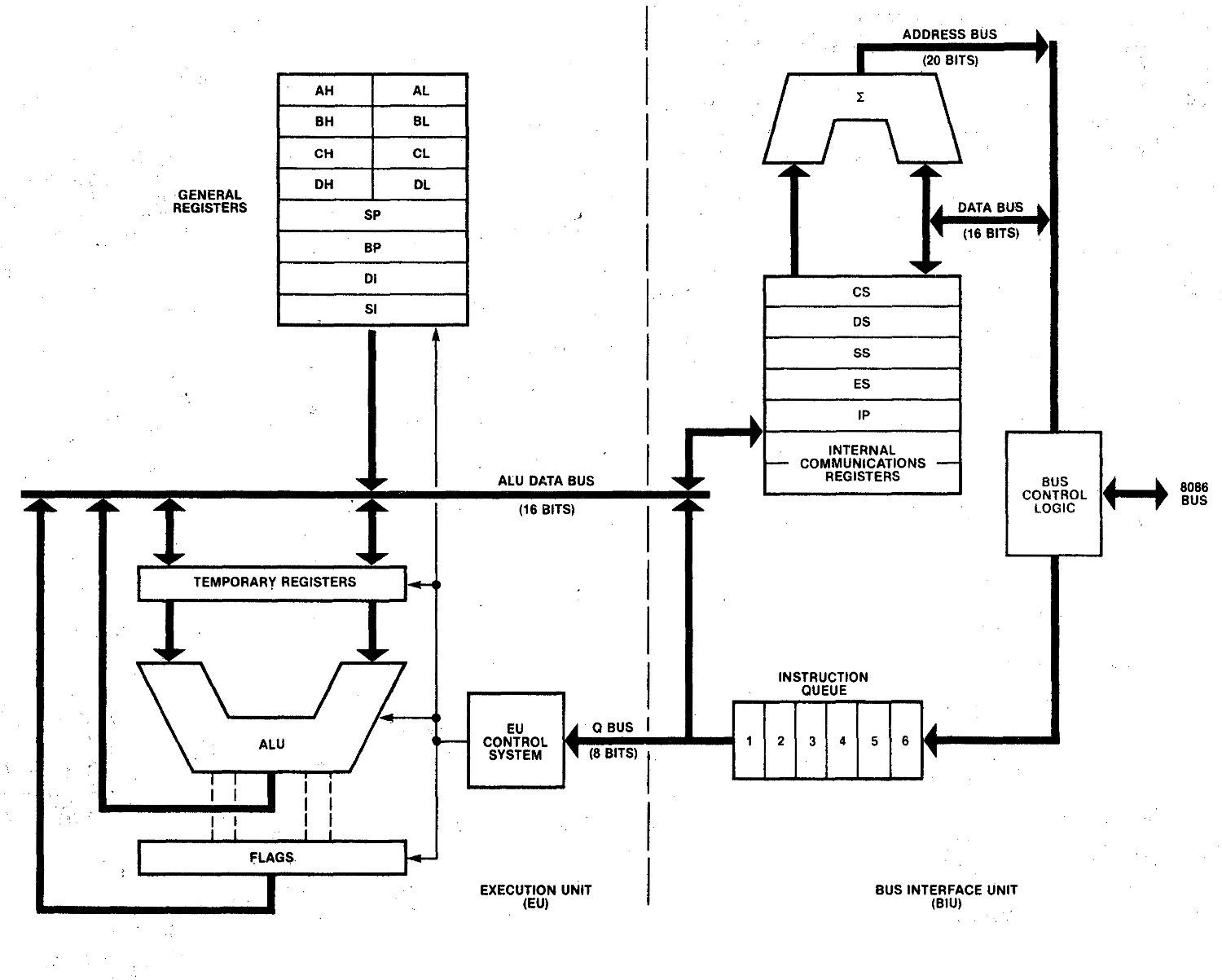
Crystal 8086. The storage location of the registers is marked. The upper registers are used by the bus interface block for memory access, while the lower general purpose registers are used by the execution block. The command buffer is a 6-byte queue of pre-requested commands.
The photo shows an image of the 8086 processor under a microscope. A metal layer is visible on top of the chip, under which silicon is hidden. Located on the outer edge of the connecting wires connect the pads on the chip to the outer 40 pins of the chip.
Fifteen 16-bit 8086 registers and six bytes of the command pre-request queue ( code prefetch ) are framed . Registers occupy a significant part of the crystal, although in total they will be typed in only 36 bytes. Due to space constraints, early microprocessors had a relatively small number of registers. By comparison, modern processor chips have kilobytes of registers and megabytes of caches.
The 8086 was one of the earliest microprocessors to implement code prefetch, but the Motorola 68000 (1979) had a 4-byte prefetch buffer a little earlier. In mainframes, prefetch existed with IBM Stretch (1961), CDC 6600 (1964), and IBM System / 360 Model 91 (1966).
The number of registers in a modern processor is difficult to calculate. The only exact number I found was in the book Anatomy of a High-Speed Microprocessor"(1997), describing in detail the AMD K6 processor. Due to the renaming of registers, modern processors have much more physical registers than architectural ones (those that are visible to the programmer), and the number of physical registers is not indicated in the documentation. K6, except for eight x86 registers general purpose, there were 16 microarchitectural work registers to
rename.Processors with AVX-512 support have 32 512-bit registers, that is, 2 KB of registers are reserved for this function. In such cases, the size of the registers is even more difficult to calculate. As for the cache size, then in advanced processors its volume reaches 77 MB .
How registers are implemented in silicon
I'll start by describing how the 8086 is built from N-MOS transistors. Then I will explain how an inverter is made, how single bits are stored with inverters, and how a register is made.
The 8086, like other chips of the era, was based on N-MOS transistors. These chips consisted of a silicon substrate, into which arsenic or boron impurities were diffused to form transistors. The polysilicon conductors above the silicon formed the gates of the transistors and connected all the components to each other. The metal layer located even higher contained additional conductors. In comparison, modern processors use CMOS technology , which combines N-MOS and P-MOS transistors, and contains many metal layers.
The diagram below shows an inverterconsisting of an N-MOS transistor and a resistor. When the input voltage is low, the transistor is off, so the pull-up resistor pulls the output up. When the input voltage is high, the transistor turns on, connects the ground and the output, pulling the output down. Thus, the incoming signal is inverted.
In fact, the pull-up resistor in an N-MOS valve is a special kind of transistor. A depleted transistor behaves like a resistor while being more compact and efficient.

The diagram shows how an inverter is made from a transistor and a resistor. The photo shows the implementation on the chip. The metal layer has been removed to show the silicon and polysilicon.
The photo above shows how the 8086 inverter is physically made. The pinkish areas are silicon with impurities that make it conductive, and the copper-colored lines are polysilicon on top. The transistor appears where polysilicon intersects with silicon. Polysilicon forms the gate of the transistor, and sections of silicon on both sides provide a source and drain. A large rectangle of polysilicon forms a pull-up resistor between + 5V and the output. So the circuit of the chip is the same as that of the inverter. Circuits like these can be viewed under a microscope and reverse-engineered.
The building block of the register is two inverters in the feedback loop storing one bit (see below). If the top conductor is 0, the right inverter will output 1 to the bottom conductor. The left inverter will then output 0 to the top conductor, completing the cycle. Thus, the circuit is stable and "remembers" 0. And vice versa, if the upper conductor is 1, it will turn to 0 on the lower conductor, and back to 1 on the upper one. As a result, the chain can store 0 or 1, forming a one-bit memory.

The 8086 has two paired inverters that store one bit in a register. The circuit is stably in state 0 or 1.
Three transistors are added to the pair of inverters to create a usable register cell. One transistor selects a cell for reading, the second selects a cell for writing, and the third amplifies the signal when reading. In the center of the circuit below, two inverters store the bit. To read the bit, the current is applied to the red bus. This connects the output of the inverter to the bit line through an amplifying transistor. To write a bit, current is applied to the red line that connects the bit line to the inverters. By applying high current signals of 0 or 1 to the bit line (and, accordingly, to the stored bit), we force the inverters to switch to the desired value. Note that the bit line is used for both reading and writing.
Other processors use slightly different register locations. The 6502 uses an additional transistor in the inverter feedback loop to break the circuit when a new value is written. The Z80 writes to both inverters at the same time, which "makes it easy" to change, but requires two wires to write. The 8086 has a gain transistor in each register location for reading, while other processors read the output from both inverters and use an external differential amplifier to amplify the signal. The base cell of register 8086 consists of 7 transistors (7T), which is more than a typical static RAM cell using 6 or 4 transistors, but it uses only one bit line, not two different ones. Dynamic memory (DRAM) is much more efficient, and uses a single transistor and capacitor,however, without updating the data, it will be lost.

Schematic diagram of a register cell storing a bit. The register file is made from an array of such cells.
The register file consists of a matrix of register cells similar to the one described above. The matrix is 16 cells wide because the registers store 16-bit values. Each register is located horizontally, so the read or write bus selects all the cells of a particular register. The 16 vertical bit lines form a single bus, so all 16 bits in the selected register are read and written in parallel.
The photo below shows an enlarged general register file 8086 showing a matrix of register cells: 16 columns and 8 rows, 8 16-bit registers. Then the increment of one register location in the file is given. I will explain how this cell is implemented.

8086 ( 16- ), . , .
The 8086 is made from doped silicon and polysilicon conductors with metal conductors on top. The left photo below shows the vertical metal conductors of the register cell. Ground, power, and bit bus wires are marked (the remaining wire crosses the register file, but does not contact it). In the photo on the right, the metal layer is dissolved so that polysilicon and silicon can be seen. The read and write buses are horizontal polysilicon conductors. Since the chip has only one metal layer, metal is used in the registers for vertical buses, and polysilicon for horizontal buses, so that they do not intersect with each other). Metal and silicon through joints show up as brighter circles in the metal photo and as circles in the silicon photo.
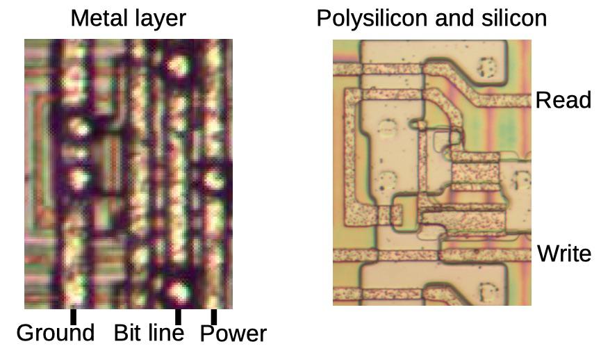
Register storage location. The photo on the left shows the metal layer, and on the right - the corresponding layers of polysilicon and silicon.
The diagram below shows the correspondence of the physical scheme of the register cell to the principal one. Inverters consist of transistor A and B and registers. Transistors C, D and E are formed by marked polysilicon pieces. The bit line is not visible because it is located in the metal layer. Note that the memory cell layout is heavily optimized to minimize size. Also note that transistor A is much smaller than the others. Inverter A has a fairly low output current, so the bit line can overcome it when writing.
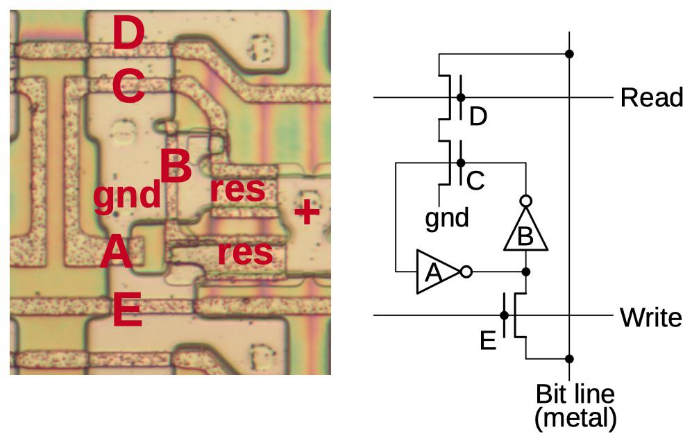
Register cell from 8086 with the corresponding circuit
Support for 8-bit registers
If you look closely at the crystal, you can see that some of the register cells have a slightly different structure. On the left is the register location we have already discussed, and on the right is a pair of register locations with two write buses instead of one. In the left photo, the write bus crosses the silicon in both register cells. In the right photo, the “right write” bus crosses the silicon on the right, but runs between the silicon on the left. Conversely, the "left write" line crosses the silicon on the left side and runs between the silicon regions on the right. Thus, one bus controls the writing of the right bit, while the other controls the writing of the left. In a 16-bit register, the interleaved 8-bit parts can be written separately in this way.
The register cell on the crystal is not repeated uniformly - every second cell is a mirror image of the previous one. This increases the density of the register cell — the power rail running between the two mirrored cells can power both of them (the same goes for ground). Mirrored repetitions reduce the number of power and ground rails required in half.
Although the block diagrams usually show how 16-bit registers are divided into left and right halves, in the real world the bits on each side alternate, instead of always storing the first 8-bit part on the left and the second on the right. This implementation simplifies the sometimes arising task of swapping two halves of a 16-bit word. One such case is reading or writing memory without alignment. Another is an ALU operation that uses the upper part of the register - for example, AH. Swapping the bits between the right and left halves would require pulling long wires between all the bits of the word halves. However, in an alternating arrangement, to swap two halves of a word, each pair of adjacent bits must be swapped, for which long wires are not needed. In other words,the 8086's interleaved register makes it easy to lay out the conductors to swap the two halves of a word.
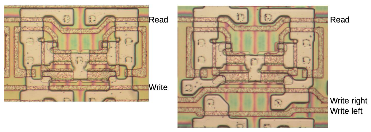
Two pairs of memory cells with different circuits. The cells on the left have one write bus, and the right ones have separate write buses for the left and right bits.
Why do some registers have two write buses and others have one? The reason is that the 8086 has 16-bit registers, but four of them can be accessed as 8-bit as shown below. For example, 16-bit accumulator A can be accessed as 8-bit AH (high-order part of accumulator) and 8-bit AL (low part) registers. Implementation of registers with two write control buses allows writing to each half of the register separately.
If the register file only supported 16-bit registers instead of 8-bit, the processor might work, but less efficiently. Writes to 8-bit halves would be done by reading all 16 bits, changing the 8-bit half, and writing all 16 bits. As a result, instead of accessing one register, the call would go to three. In this case, the register file does not need to somehow particularly support reading 8 bits, since the unnecessary half can simply be ignored.

General Purpose Registers in the 8086. Registers A, B, C, and D can be divided into two 8-bit halves.
Multiport registers
So far we've covered eight general-purpose "lower registers". The 8086 also has seven "upper registers" used for memory access, including the infamous segment registers . These registers have a more complex, multi-port scheme of operation, allowing several read and write processes to be carried out simultaneously. For example, a multiport register file allows you to read a program counter, a segment register, and write another segment register, all at the same time.
The block diagram below is different from most block diagrams.for 8086, because it shows the real physical implementation of the processor, and not what the programmer imagines. In particular, the diagram shows two "internal communication registers" among the registers of the bus interface module (right), along with segment registers that match the 7 registers that can be seen on the chip. The temporary registers shown below are physically part of the ALU, so I will not cover them in this article.
The book " Designing Modern Processors " discusses complex register systems in a processor since the 2000s. It says that circuit complexity quickly goes beyond three ports, and some advanced processors have register files with 20 or more ports.
The multiport register cell below is based on the same two-inverter circuit, however it has three bit lines (not one as in the previous case) and five control lines (instead of two). Three read buses allow you to read the contents of a register cell on any of the three bit lines, and two write buses allow bit A or C to write to a register cell.
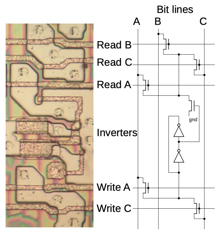
Multiport register cell in 8086 processor
At first glance, the 8086 register file looks like a homogeneous set of registers, but a closer look shows that each register is optimized depending on its function. Some of them are simple 16-bit registers and are most compactly located. The other 16-bit registers can be accessed as two 8-bit registers, which requires another control bus. The most complex registers have two to three ports for reading and one or two for writing. In each case, the physical implementation of the register cell is carefully designed to take up as little space as possible, and therefore the shape of the transistors is often complex. Intel engineers squeezed the register layout as tightly as possible to fit all of them in the space available to them.
The upper registers have a different number of ports for reading and writing: two registers with 3 read and 2 write buses, one register with 2 read and 2 write buses, four registers with 2 read and 1 write buses. The first three registers are probably the program counter, an indirect temporary register, and a temporary operand register. The last four are probably the SS, DS, SS, and ES segment registers. There are also three instruction prefetch buffer registers, each with one read and one write bus.
The 8088 processor used in the original IBM PCs was virtually identical to the 8086, except that it had an 8-bit external bus instead of a 16-bit one, so the system was less expensive. The 8088's prefetch buffer was 4 bytes instead of 6 - probably because 4 bytes was enough for the 8088's slower memory bus.
Unlike the 8086, the 8088's prefetch registers support independent writing to 8-bit halves (similar to the 8088's A, B, C, and D registers, only these cells look different). This is because the 8088 requested commands one byte at a time, and not one word at a time, due to the narrow bus. Therefore, prefetch registers must support byte writing, while the 8086 supports word prefetch.
Upper register file consisting of ten 16-bit registers. The photo shows silicon and polysilicon. Vertical red lines - remnants of the removed metal layer. Clickable.
Conclusion
Although the 8086 processor is 42 years old, it still has a significant impact on modern computers, as the x86 architecture is still very commonly used today. Registers 8086 still exist in modern x86 computers, although today they are already 64 bits long, and besides these registers there are many others.
The 8086 crystal is very interesting to study because its transistors can be viewed under a microscope. At one time it was a complex processor, with 29,000 transistors on it, but simple enough to trace all the circuits and understand how they work.
See also:
- " Chip Scaling: How Intel Scaled the 8086 Processor "
- " Reverse engineering of the Intel 8086 microprocessor "
- " Analysis of the shift register crystal of the 8087 mathematical coprocessor "