Background and first samples
In an old post I wrote that I was working on reverse engineering the PLA chip of the Commodore 128. Now I have almost completed this process, so it's time to share my findings.
It was a very interesting project because I didn't know much about designing and manufacturing semiconductors. My knowledge was limited to looking at pictures of crystals and admiring these beautiful photographs.
For me, my research began with the purchase of a cheap microscope for soldering surface mount (SMD) components.
Cheap microscope
After some time, I found a video on Youtube showing an easier way to remove silicon crystals from a case.
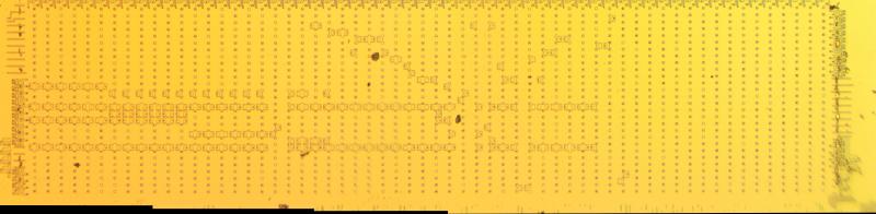
The method looked simple enough to implement at home, because I already had all the necessary equipment. Removing an IC from a package usually requires heated sulfuric acid or other hazardous chemicals that I didn't really want to experiment with at home. So I dug up a couple of broken MOS chips in my inventory (never throw anything away, it might come in handy). With a little work, I got two 8521R0 dies and one 8721 PLA. In the previous post, I showed the first real photo.
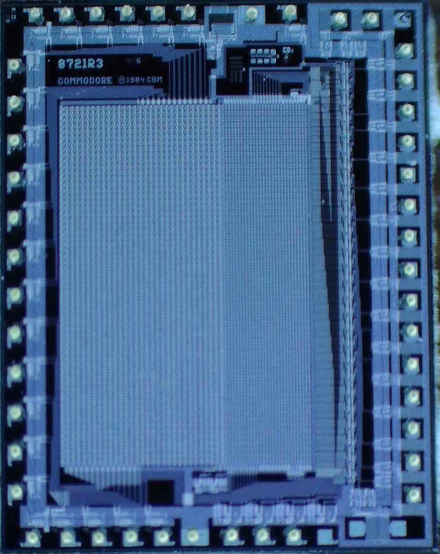
Full photo of the 8721 PLA chip
Better microscope
Although the experiment was successful, I immediately realized that the microscope did not have enough resolution to take pictures with sufficient quality for me. With a 2x Barlow lens, the maximum magnification is 90x. In addition, the microscope does not have a stage, so I had to place the crystal on the table and then move the entire microscope; this design is very unstable and it is difficult to remove the necessary parts with its help.
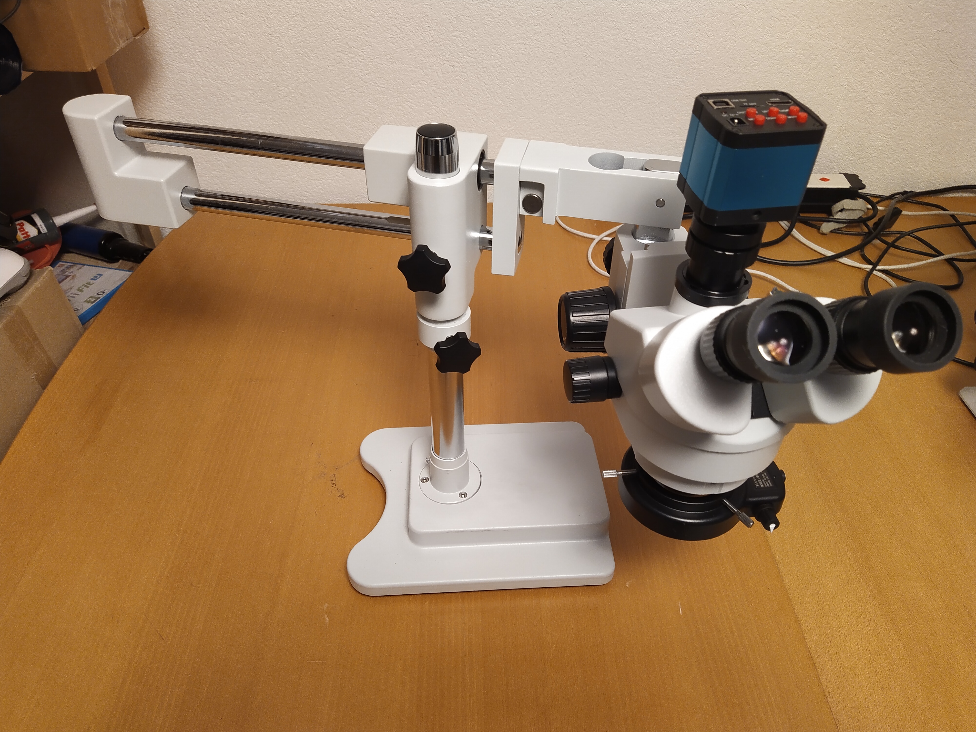
So I found and bought a better microscope, also for a reasonable price.
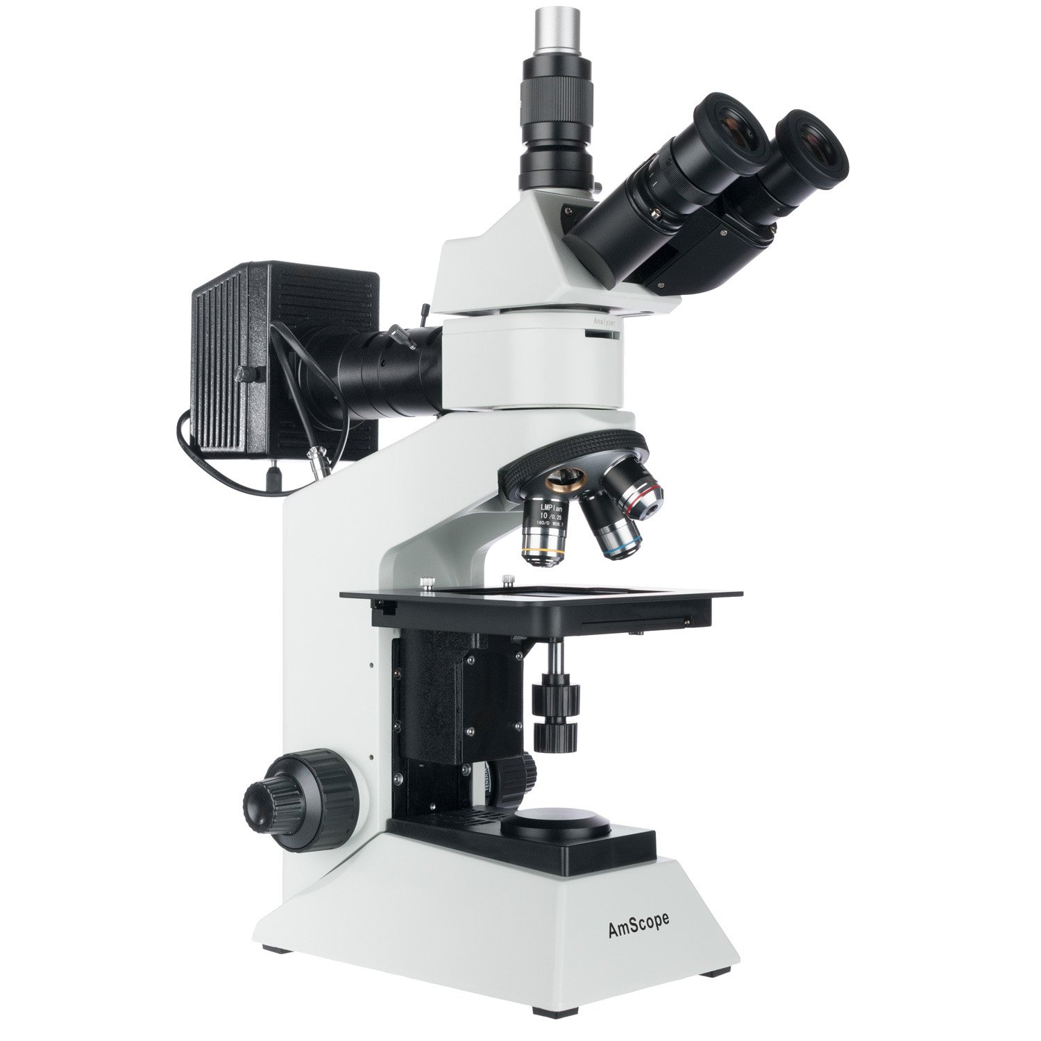
AmScope ME580-T microscope It did a
much better job of taking decent quality photos, but I was not happy with the camera I bought with it. This is a cheap camera with no remote control, except for the AmScope application. At that time, the Raspberry Pi foundation released a new high quality camera for the Raspberry Pi. This camera has a C-mount compatible with the microscope, so I immediately bought it and installed it on the microscope. It does an amazing job of providing complete control from the comfort of Linux.
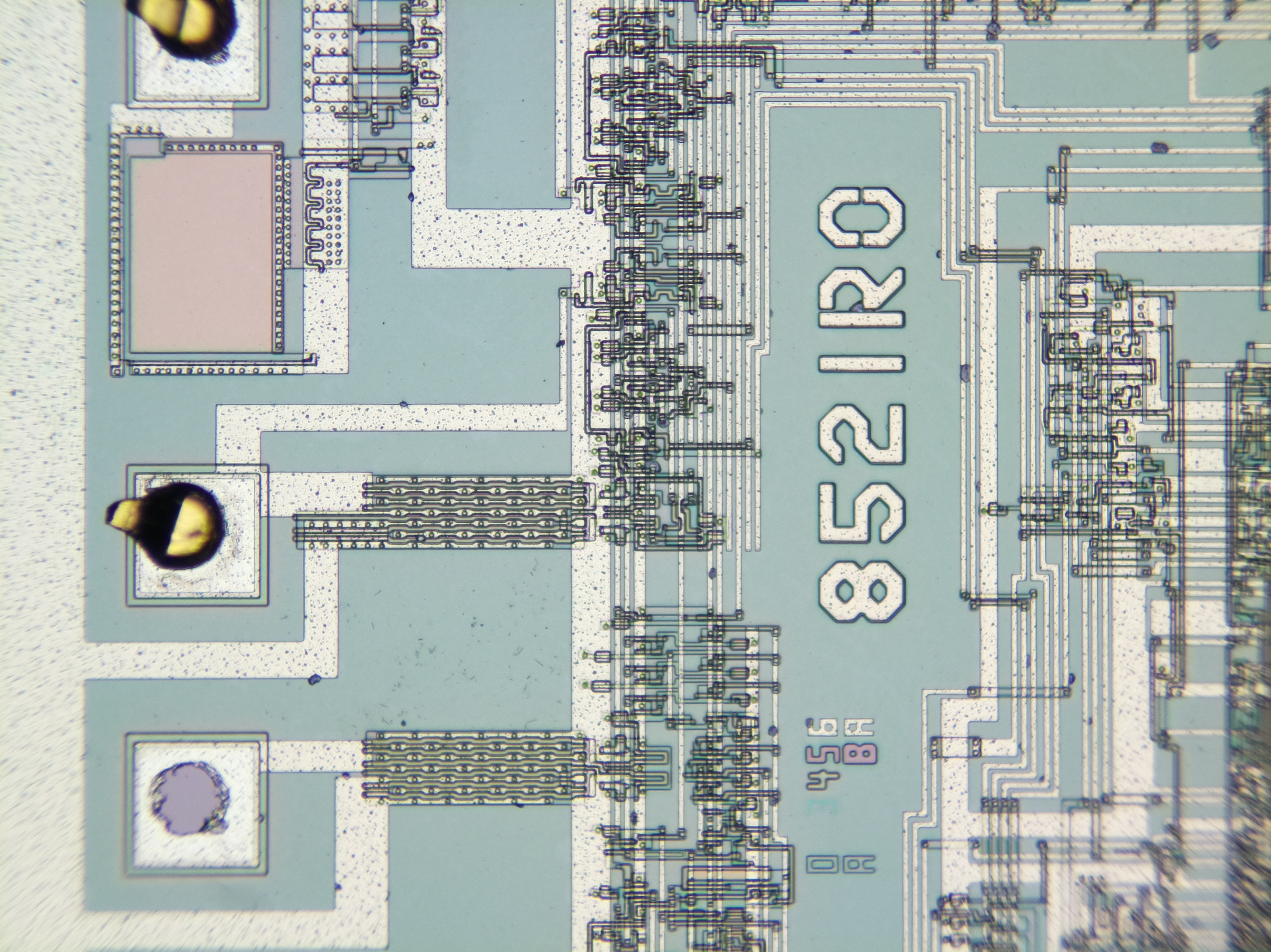
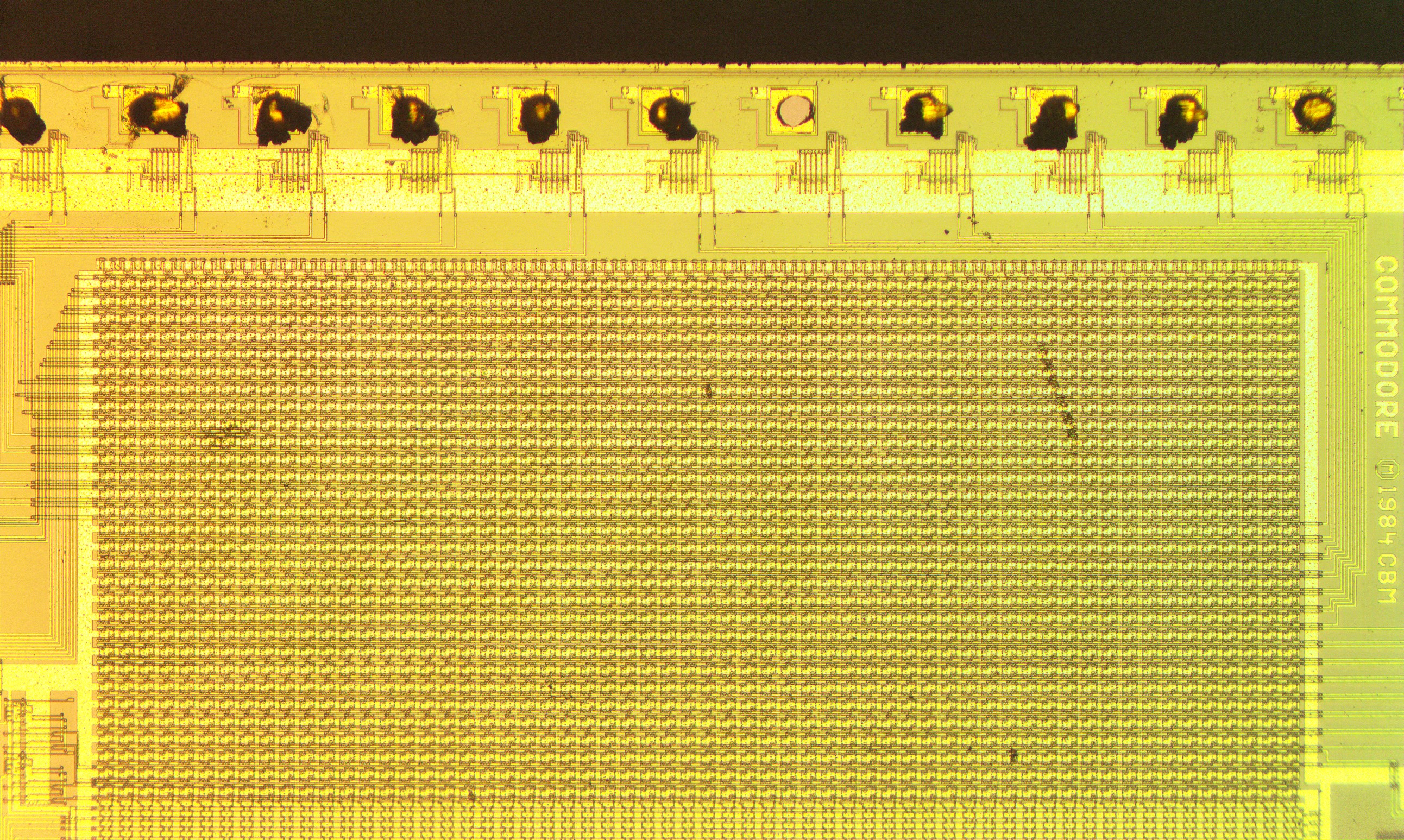
Part of silicon die 8521R0
Compared to the previous system, this is a huge improvement. Due to the increased resolution, I had to stitch the photos to get larger images. It sounds simple at first, but it turned out (as you might have guessed) not an easy task at all. I still have difficulty stitching photos together, but I am gradually improving my skill. One of the key factors for a successful panoramic shot is uniformity in focus, white balance, etc. The more uniform the photographs are, the easier and better the stitching becomes.
Mechanization
All this made me start mechanizing the table. I began to get very tired of manually moving the table, in which the photos were displaced along several axes and other distortions occurred.
After doing a lot of design, 3D printing and CNC firmware research, I came up with the following design:
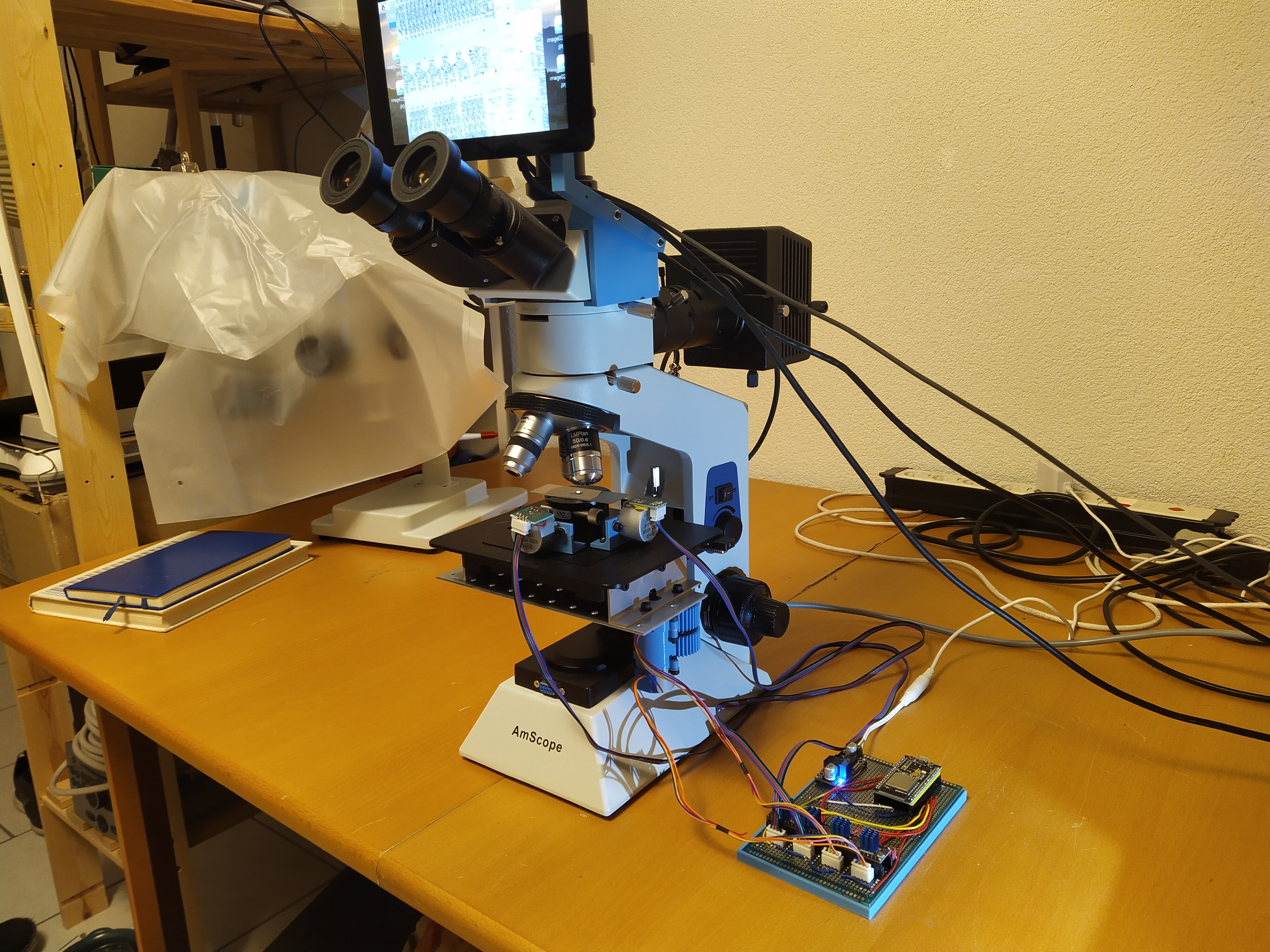
Modified microscope AmScope ME580-T
On top there is a 7-inch Raspberry display, behind which is a Raspberry Pi4. The photo does not show the RPi HiQ camera mounted on the microscope. The RPi takes photos, displays them on the display, and also executes the Python code that drives the CNC board.
The subject stage and leveling stage are driven by 28BYJ-48 stepper motors, which are driven by a small ESP32 board running Grbl_Esp32 , as well as four AD4498 stepper motor controllers.
The circuit has certain software and hardware problems, but it works quite well for my purposes.
Reverse the chip
Having dealt with the logistics, I went back to reverse engineering the chip itself. I originally wanted to tackle the PLA chip because it would be the easiest thing to figure out. PLA stands for Programmable Logic Array ; similar structures were very common in the Commodore era.
Based on the schematic from Wikipedia, we should expect that there are two main arrays on the chip, AND and OR. Inputs are connected to AND and pins come out of the OR array.
Going back to the previous shot of the die, we can improve it by adding annotations to the pins and areas of the chip. Having dealt with the purpose of the crystals, we can see that all inputs are connected to one array, and all outputs are connected to another, as expected. also, it will help us understand where is which array.
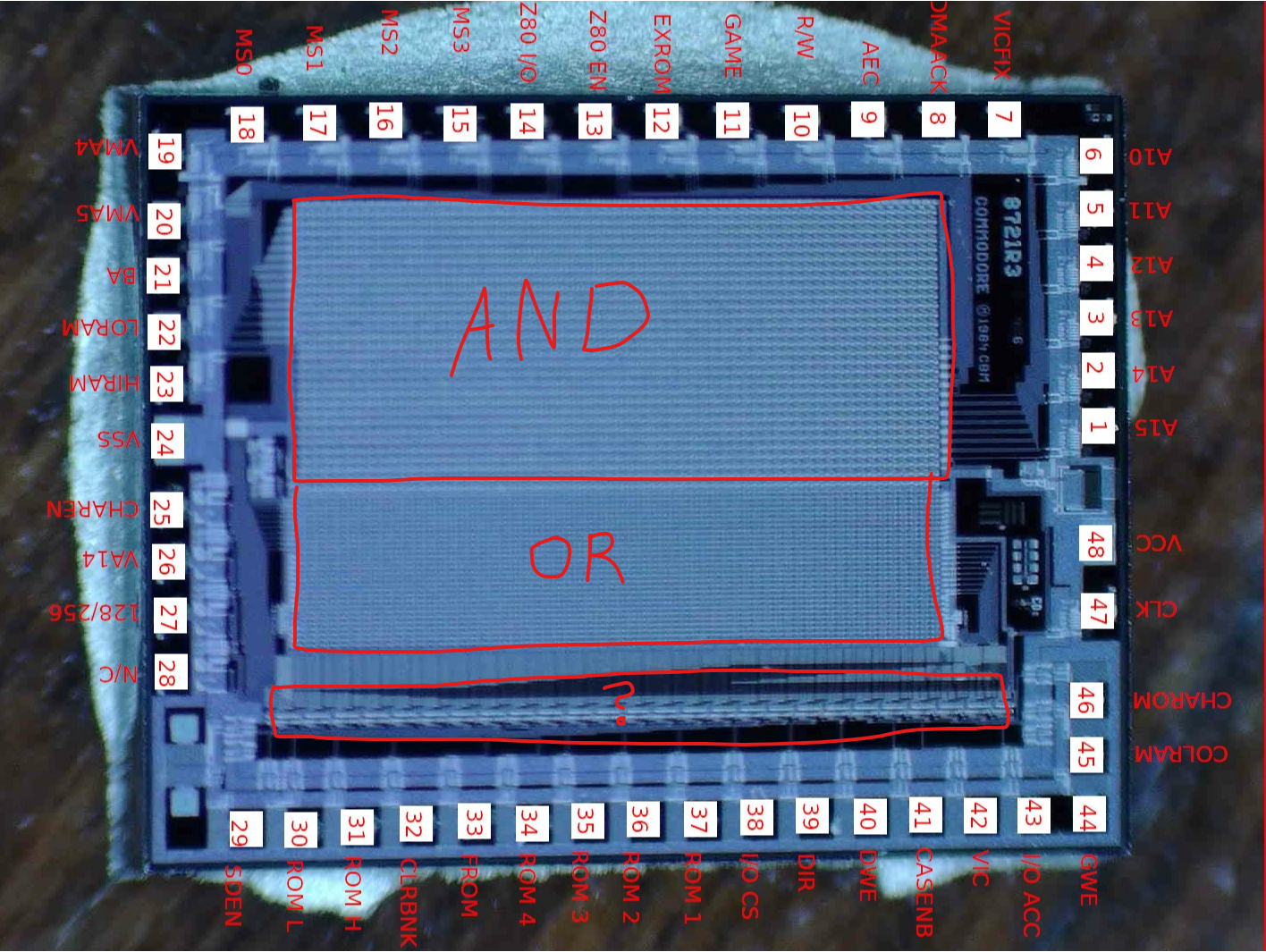
Snapshot of 8721 PLA die with annotations
Here we see the marked I / O pins and their connection to the lead frame and to the pins of the DIP itself. Also visible are the two main areas that make up the PLA structure, the AND array and the OR array. Also, there is some additional logic down here marked with a question mark. Its purpose was unknown to me, but since all output contacts pass through it, I assumed that this was some kind of output stage.
AND array
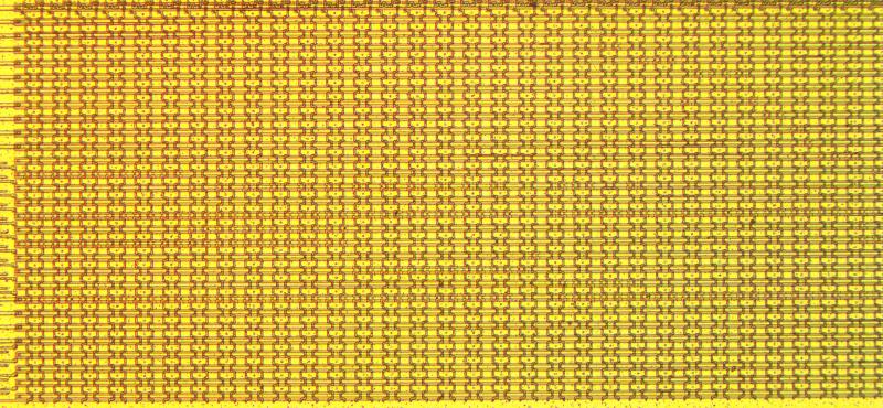
So, if we first start to examine the AND matrix more closely, we will see the picture below. The colors are a little distorted, because this picture was taken with an AmScope camera and I could not figure out how to set the white balance on it.
AND Matrix with metal layer
The image is not very useful for understanding what is happening because all the interesting parts are covered by the topmost metal layer. I was just starting to learn back then, so I used brute force to remove the metal. I erased the metal by strong mechanical impact; after studying under a microscope, it turned out that everything was removed in general, except for the substrate itself.
Fortunately, the details I needed were in the diffusion layer located in the substrate:

Matrix substrate AND
Looking closely at the image, you can see small wavy lines where the transistor is located to create a connection in the matrix.
OR array
Moving on to the OR array, we see exactly the same format. Difficult to parse without removing the metal layer, but easier compared to the AND matrix. And it is much easier when only the substrate and the diffusion layer are left.
OR die with metal layer
OR Matrix Substrate
Full matrix decoding
Armed with this knowledge, we can proceed to recover the full PLA logic matrix from images.
I marked all transistors in each matrix with dots and got the following image:
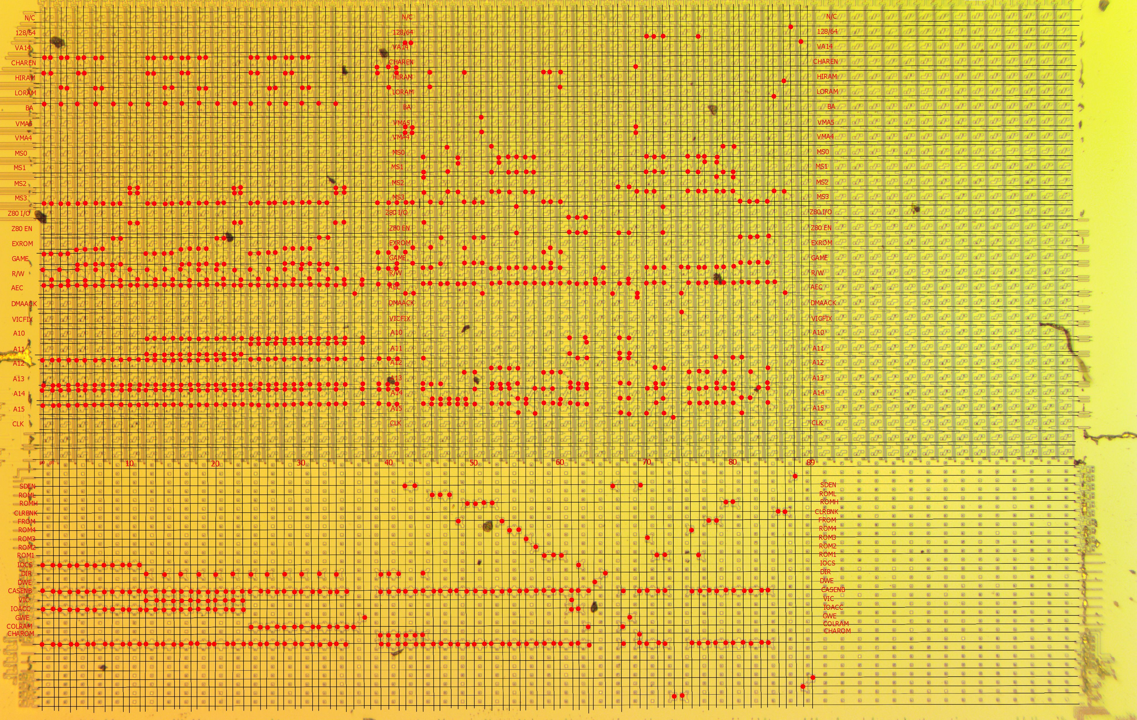
An AND Matrix with a Metal Layer
In an AND matrix, all inputs are horizontal, and a normal and inverted signal is fed to each line. In an OR matrix, all leads are horizontal and connected to vertical lines called minterms.
After examining the points, we can decode the minterms by performing the logic "AND" for all vertical lines in the AND matrix, for example
p0 = CHAREN & HIRAM & BA & !MS3 & GAME & RW & AEC & A12 & !A13 & A14 & A15
For pins, we take a horizontal line for each pin and combine it with “or”, for example
SDEN = p42 | p43 | p66 | p69
This is how we got the whole set of logical equations. Hooray!
Output stage
Let's go back to the complete photo of the crystal - now we have everything except the rectangle marked with a question mark on the exit path.
Looking at the higher resolution photographs of this area, we see similar patterns for each pin. In all but two cases, this structure is bypassed and the output from the OR matrix goes directly to the output pin. However, this does not apply to two contacts:
DWEand CASENB.
DWEIs the Write Enable signal applied to the DRAM chips of the main system, and CASENB passes the CAS signal to the RAM. These two signals are somehow processed by these output gate structures, so I needed to reverse engineer this block.

Outlet block with metal layer
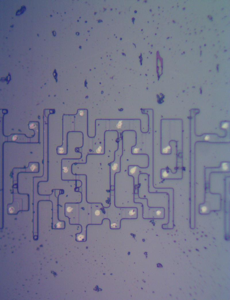
Output Block Substrate
After spending quite a lot of time reading information about the design and manufacturing of silicon chips, as well as making many attempts, I was able to create a logical-looking circuit. I will not go into detail about the whole process here, but will document and publish it later. Here I would also like to thank Frank Wolfe for his help, if possible, support his project!
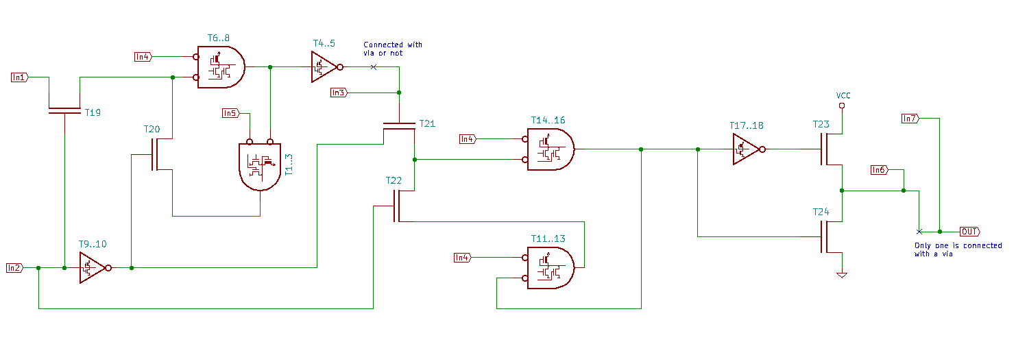
Output Block Circuit
Looking a little further, the way this circuit is used is with pins
DWEand CASENBturns it into a regular D-latch. The latch that allows this is represented in the PLA by a pair of lines in the OR.
Result
So we got the final result and now we can write the complete HDL code for the PLA chip of the C128 computer. For this, I will use Verilog. Consider. that this is my first Verilog code, so it may not be optimal. Using a D-latch for a pin is generally considered bad practice in Verilog, but in this case I am replicating the logic and functionality of the finished chip.
I checked it if possible, but if I am missing something, please report it!
Unlike the PLA C64, the PLA C128 chip cannot be replaced with just an EPROM or something similar due to the presence of output latches.
module pla_8721(
    input rom_256,
    input va14,
    input charen,
    input hiram,
    input loram,
    input ba,
    input vma5,
    input vma4,
    input ms0,
    input ms1,
    input ms2,
    input ms3,
    input z80io,
    input z80en,
    input exrom,
    input game,
    input rw,
    input aec,
    input dmaack,
    input vicfix,
    input a10,
    input a11,
    input a12,
    input a13,
    input a14,
    input a15,
    input clk,

    output sden,
    output roml,
    output romh,
    output clrbnk,
    output from,
    output rom4,
    output rom3,
    output rom2,
    output rom1,
    output iocs,
    output dir,
    output reg dwe,
    output reg casenb,
    output vic,
    output ioacc,
    output gwe,
    output colram,
    output charom);

wire p0;
wire p1;
wire p2;
wire p3;
wire p4;
wire p5;
wire p6;
wire p7;
wire p8;
wire p9;
wire p10;
wire p11;
wire p12;
wire p13;
wire p14;
wire p15;
wire p16;
wire p17;
wire p18;
wire p19;
wire p20;
wire p21;
wire p22;
wire p23;
wire p24;
wire p25;
wire p26;
wire p27;
wire p28;
wire p29;
wire p30;
wire p31;
wire p32;
wire p33;
wire p34;
wire p35;
wire p36;
wire p37;
wire p38;
wire p39;
wire p40;
wire p41;
wire p42;
wire p43;
wire p44;
wire p45;
wire p46;
wire p47;
wire p48;
wire p49;
wire p50;
wire p51;
wire p52;
wire p53;
wire p54;
wire p55;
wire p56;
wire p57;
wire p58;
wire p59;
wire p60;
wire p61;
wire p62;
wire p63;
wire p64;
wire p65;
wire p66;
wire p67;
wire p68;
wire p69;
wire p70;
wire p71;
wire p72;
wire p73;
wire p74;
wire p75;
wire p76;
wire p77;
wire p78;
wire p79;
wire p80;
wire p81;
wire p82;
wire p83;
wire p84;
wire p85;
wire p86;
wire p87;
wire p88;
wire p89;

wire casenb_int;
wire casenb_latch;

/* Product terms */

assign p0 = charen & hiram & ba & !ms3 & game &  rw & aec & a12 & !a13 & a14 & a15;
assign p1 = charen & hiram &      !ms3 & game & !rw & aec & a12 & !a13 & a14 & a15;
assign p2 = charen & loram & ba & !ms3 & game &  rw & aec & a12 & !a13 & a14 & a15;
assign p3 = charen & loram &      !ms3 & game & !rw & aec & a12 & !a13 & a14 & a15;

assign p4 = charen & hiram & ba & !ms3 & !exrom & !game &  rw & aec & a12 & !a13 & a14 & a15;
assign p5 = charen & hiram &      !ms3 & !exrom & !game & !rw & aec & a12 & !a13 & a14 & a15;
assign p6 = charen & loram & ba & !ms3 & !exrom & !game &  rw & aec & a12 & !a13 & a14 & a15;
assign p7 = charen & loram &      !ms3 & !exrom & !game & !rw & aec & a12 & !a13 & a14 & a15;

assign p8 = ba & !ms3 & exrom & !game & rw & aec & a13 & !a13 & a14 & a15;
assign p9 =      !ms3 & exrom & !game & rw & aec & a12 & !a13 & a14 & a15;

assign p10 = ba & !ms2 & ms3 &  rw & aec & a12 & !a13 & a14 & a15;
assign p11 =      !ms2 & ms3 & !rw & aec & a12 & !a13 & a14 & a15;

assign p12 = charen & hiram & ba & !ms3 & game &  rw & aec & !a10 & !a11 & a12 & !a13 & a14 & a15;
assign p13 = charen & hiram &      !ms3 & game & !rw & aec & !a10 & !a11 & a12 & !a13 & a14 & a15;
assign p14 = charen & loram & ba & !ms3 & game &  rw & aec & !a10 & !a11 & a12 & !a13 & a14 & a15;
assign p15 = charen & loram &      !ms3 & game & !rw & aec & !a10 & !a11 & a12 & !a13 & a14 & a15;

assign p16 = charen & hiram & ba & !ms3 & !exrom & !game &  rw & aec & !a10 & !a11 & a12 & !a13 & a14 & a15;
assign p17 = charen & hiram &      !ms3 & !exrom & !game & !rw & aec & !a10 & !a11 & a12 & !a13 & a14 & a15;
assign p18 = charen & loram & ba & !ms3 & !exrom & !game &  rw & aec & !a10 & !a11 & a12 & !a13 & a14 & a15;
assign p19 = charen & loram &      !ms3 & !exrom & !game & !rw & aec & !a10 & !a11 & a12 & !a13 & a14 & a15;

assign p20 = ba & !ms3 & exrom & !game & rw & aec & !a10 & !a11 & a12 & !a13 & a14 & a15;
assign p21 =      !ms3 & exrom & !game & rw & aec & !a10 & !a11 & a12 & !a13 & a14 & a15;

assign p22 = ba & !ms2 & ms3 &  rw & aec & !a10 & !a11 & a12 & !a13 & a14 & a15;
assign p23 =      !ms2 & ms3 & !rw & aec & !a10 & !a11 & a12 & !a13 & a14 & a15;

assign p24 = charen & hiram & ba & !ms3 & game &  rw & aec & !a10 & a11 & a12 & !a13 & a14 & a15;
assign p25 = charen & hiram &      !ms3 & game & !rw & aec & !a10 & a11 & a12 & !a13 & a14 & a15;
assign p26 = charen & loram & ba & !ms3 & game &  rw & aec & !a10 & a11 & a12 & !a13 & a14 & a15;
assign p27 = charen & loram &      !ms3 & game & !rw & aec & !a10 & a11 & a12 & !a13 & a14 & a15;

assign p28 = charen & hiram & ba & !ms3 & !exrom & !game &  rw & aec & !a10 & a11 & a12 & !a13 & a14 & a15;
assign p29 = charen & hiram &      !ms3 & !exrom & !game & !rw & aec & !a10 & a11 & a12 & !a13 & a14 & a15;
assign p30 = charen & loram & ba & !ms3 & !exrom & !game &  rw & aec & !a10 & a11 & a12 & !a13 & a14 & a15;
assign p31 = charen & loram &      !ms3 & !exrom & !game & !rw & aec & !a10 & a11 & a12 & !a13       & a15;

assign p32 = ba & !ms3 & exrom & !game & rw & aec & !a10 & a11 & a12 & !a13 & a14 & a15;
assign p33 =      !ms3 & exrom & !game & rw & aec & !a10 & a11 & a12 & !a13       & a15;

assign p34 = ba & !ms2 & ms3 &  rw & aec & !a10 & a11 & a12 & !a13 & a14 & a15;
assign p35 =      !ms2 & ms3 & !rw & aec & !a10 & a11 & a12 & !a13       & a15;

assign p36 = !aec;
assign p37 = !rw & aec & !a10 & a11 & a12 & !a13 & a15;

assign p39 = !charen & hiram & !ms3 &           game & rw & aec & a12 & !a13 & a14 & a15;
assign p40 = !charen & loram & !ms3 &           game & rw & aec & a12 & !a13 & a14 & a15;
assign p41 = !charen & hiram & !ms3 & !exrom & !game & rw & aec & a12 & !a13 & a14 & a15;

assign p42 = va14 & !vma5 & vma4 & !ms3          &  game & !aec;
assign p43 = va14 & !vma5 & vma4 & !ms3 & !exrom & !game & !aec;

assign p44 = !ms0 & !ms1 & ms2 &ms3 & z80en & rw & aec & a12 & !a13 & a14 & a15;
assign p45 = hiram & loram & !ms3 & !exrom & rw & aec & !a13 & !a14 & a15;

assign p46 = !ms3 & exrom & !game & aec & !a13 & !a14 & a15;
assign p47 = ms0 & !ms1 & ms3 & exrom & !game & aec & !a14 & a15;
assign p48 = !ms0 & ms1 & ms3                 & aec & !a14 & a15;

assign p49 = hiram & !ms3 & !exrom & !game & aec & a13 & !a14 & a15;
assign p50 = ms3 & exrom & !game & aec & a13 & !a14 & a15;

assign p51 = vma5 & vma4 & !ms3 & exrom & !game & !aec;
assign p52 =  ms0 & !ms1 & ms3 & rw & aec & !a12 & !a13 & a14 & a15;
assign p53 = !ms0 &  ms1 & ms3 & rw & aec & !a12 & !a13 & a14 & a15;
assign p54 = !ms0 & !ms1 & ms3 & rw & aec & !a12 & !a13 & a14 & a15;

assign p55 = !ms0 & !ms1 & z80io & !z80en & rw & aec & !a12 & !a13 & !a14 & !a15;
assign p56 = !ms0 & !ms1 & ms3 & rw & aec & !a14 &  a15;
assign p57 = !ms0 & !ms1 & ms3 & rw & aec &  a14 & !a15;

assign p58 = hiram         & !ms3          &  game & rw & aec & a13 &  a14 & a15;
assign p59 = hiram         & !ms3 & !exrom & !game & rw & aec & a13 &  a14 & a15;
assign p60 = hiram & loram & !ms3          &  game & rw & aec & a13 & !a14 & a15;

assign p61 = !z80io & !z80en & aec & !a10 & !a11        & !a13 & a14 & a15;
assign p62 = !z80io & !z80en & aec               &  a12 & !a13 & a14 & a15;
assign p63 = !z80io & !z80en & aec & !a10 &  a11 &  a12 & !a13 & a14 & a15;

assign p64 = !rw & aec;
assign p65 =  rw & aec;
assign p66 = !aec;

assign p67 = !ms2 & !z80en       & aec & !a10 & !a11 & a12 & !a13 & !a14 & !a15;
assign p68 = !ms2 & !z80en & !rw & aec & !a10 & !a11 & a12 & !a13 & !a14 & !a15;

assign p69 = !charen & !vma5 & vma4 & ms3 & aec;

assign p70 = !rom_256 & !ms0 & !ms1 & ms3 & rw & aec               & a14 & !a15;
assign p71 = !rom_256 & !ms0 & !ms1 & ms3 & rw & aec & !a12 & !a13 & a14 &  a15;
assign p72 = !rom_256 & !ms0 & !ms1 & z80io & !z80en & rw & aec & !a12 & !a13 & !a14 & !a15;

assign p73 = clk;
assign p74 = rw & !aec & vicfix;

assign p75 =            !ms0 & !ms1       & ms3 & rw & aec       &  a13 & a14 & a15;
assign p76 = !rom_256 & !ms0 & !ms1       & ms3 & rw & aec       &  a13 & a14 & a15;
assign p77 =            !ms0 &  ms1       & ms3 & rw & aec       &  a13 & a14 & a15;
assign p78 =            !ms0 &  ms1 & ms2 & ms3 & rw & aec & a12 & !a13 & a14 & a15;
assign p79 =             ms0 & !ms1       & ms3 & rw & aec       &  a13 & a14 & a15;
assign p80 =             ms0 & !ms1 & ms2 & ms3 & rw & aec & a12 & !a13 & a14 & a15;

assign p81 = !ms3 & exrom & !game & aec &  a12        & !a14 & !a15;
assign p82 = !ms3 & exrom & !game & aec        &  a13 & !a14;
assign p83 = !ms3 & exrom & !game & aec               &  a14;
assign p84 = !ms3 & exrom & !game & aec & !a12 & !a13 &  a14 &  a15;

assign p85 = !loram & ms3 &  aec;
assign p86 = !hiram & ms3 & !aec;

/* outputs */

assign sden = p42 || p43 || p66 || p69;
assign roml = p45 || p46 || p47;
assign romh = p49 || p50 || p51 || p52 || p79 || p80;
assign clrbnk = p85 || p86;
assign from = p48 || p53 || p77 || p78;
assign rom4 = p54 || p55 || p75;
assign rom3 = p56 || p70;
assign rom2 = p57;
assign rom1 = p58 || p59 || p60 || p71 || p71 || p76;
assign iocs = p0 || p1 || p2 || p3 || p4 || p5 || p6 || p7 || p8 || p9 || p10 || p11 || p62;
assign dir = p12 || p14 || p16 || p18 || p20 || p22 || p24 || p26 || p28 || p30 || p32 || p34 || p39 || p40 || p41 || p44 || p65;
assign vic = p12 || p13 || p14 || p15 || p16 || p17 || p18 || p19 || p20 || p21 || p22 || p23 || p61;
assign ioacc = p0 || p1 || p2 || p3 || p4 || p5 || p6 || p7 || p8 || p9 || p10 || p11 ||
               p12 || p13 || p14 || p15 || p16 || p17 || p18 || p19 || p20 || p21 || p22 || p61 || p62;
assign gwe = p37;
assign colram = p24 || p25 || p26 || p27 || p28 || p29 || p30 || p31 || p32 || p33 || p34 || p35 || p36 || p63 || p67;
assign charrom = p39 || p40 || p41 || p42 || p43 || p44 || p69;

assign casenb_latch = p73 || p74;

assign casenb_int = p0 || p1 || p2 || p3 || p4 || p5 || p6 || p7 || p8 || p9
                || p10 || p11 || p12 || p13 || p14 || p15 || p16 || p17 || p18 || p19
                || p20 || p21 || p22 || p23 || p39 || p40 || p41 || p42 || p43 || p44
                || p45 || p46 || p47 || p48 || p49 || p50 || p51 || p52 || p53 || p54
                || p55 || p56 || p57 || p58 || p59 || p60 || p61 || p62 || p63 || p67
                || p69 || p70 || p71 || p72 || p75 || p76 || p77 || p78 || p79 || p80
                || p81 || p82 || p83 || p84;

/* Latched outputs */

always @ (clk or p64)
  if (clk)
    dwe <= p64;

always @ (casenb_latch or casenb_int)
  if (casenb_latch)
    casenb <= casenb_int;

endmodule
What's next
The next analyzed chip will be the C128 computer MMU chip, which will take much longer to work on, because it is not just ordinary PLA.
See also:
- « The Commodore the Amiga 500+: Let nobody will leave offended "
- " Computer brands of the 90s "
- " Computer brands of the 90s, part 2 "