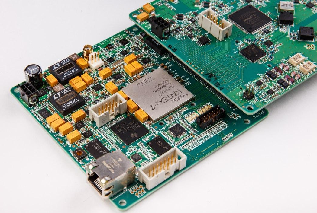
One of the most popular questions of interest to today's graduates: "Is it easy to be a technologist, designer or engineer in the production of printed circuit boards?" It would seem that everything will be told in the learning process, and shown - in production practices. But my colleagues and I agree that definitely not. To work successfully in the industrial production of electronics, you need to know such subtleties that are not taught at the university. Therefore, I decided to share my experience and the experience of my colleagues here.
But first, you need to figure out where the printed circuit board begins. Before the designer proposes his idea, and the technologists start the initial stage of production, it is necessary to determine from what material we will make the printed circuit board.
The most popular material for the production of printed circuit boards is foil-clad fiberglass, which has a laminated plastic structure, in which fibers alternate with a polymer binder. There can also be several options for such a binder: bakelite, epoxy and polyester resins. Each material has its own advantages, but I will write about them sometime later.
In the meantime, let's deal with the basic materials.
As already mentioned, one of the most popular is fiberglass. There are many brands here: CTT, STEB, STEF-P, SF, etc. And the abbreviation FR is often found in the description, meaning the fire resistance of the material, the higher the number after these letters, the more fire resistance the printed circuit board will have (there are classes of the first , second, third and even sixth durability). But most often used glass fiber laminate of normalized flammability FR-4.
And if fiberglass is a dielectric, then copper foil is used for the conductive layer, which is pressed onto glass fiber, and then galvanic copper is built up. The thickness of the copper foil layer can be any, but most often it is 12, 18, 35, 50, 70 and 105 microns. However, it is worth remembering that if you are ordering from an imported manufacturer, the thickness of the copper foil will be indicated in ounces (1 ounce per square foot equals approximately 34 microns).
In addition to fiberglass, aluminum is also used as a base material for a printed circuit board. But since, unlike fiberglass, aluminum conducts current, another layer is added between it and the copper foil - a layer of dielectric. These printed circuit boards are used in products that require large amounts of heat dissipation, such as LED lighting fixtures.
There are also base materials based on a ceramic or Teflon filler. This is a very rare group of materials, which is used mainly for the production of equipment in the aviation and space industries.
But the right material for the printed circuit board is not all that is needed for the product to be of high quality. The process of assembling the packages for drilling plays an important role here. At first glance, there is nothing complicated here, because in the base material you just need to insert pins between the lining and lining materials. But what materials you choose for the backing and backing will play a big role.
The overlay material will reduce the number of burrs, while improving the quality and accuracy of drilling and increasing the resource of the tool. In turn, the backing material also helps to reduce burrs, allows you not to smear the cut product on the work surface and helps to cool the cutting tool. The backing material should be firm but easy to drill to avoid wearing out the tool.
For printed circuit boards of a low accuracy class, you can choose getinax, phenolic paper or thin sheets of fiberglass as an overlay material. But for a higher accuracy class, it is already worth using thin aluminum sheets. They will reduce tool vibration during drilling and resin adhesion to the cutting edge of the tool. All this will help to improve drilling accuracy. However, if you need PCBs of 5th grade or higher, then ordinary aluminum sheet will not be enough either. In this case, it is worth using aluminum-based overlays covered with a lubricating layer (lubricant). This layer makes the drill less likely to slip to the side when drilling into a bag.
The lining material is wood fibers pressed under high pressure (MDF is most often used). However, they are also different, depending on the result you want.
And, of course, before you start drilling, you need to properly clean both the base and auxiliary materials. For this, you can use conventional anti-static rolls with sticky paper.
As you probably already understood, it is not so easy to work in PCB manufacturing. Even the simplest process can have so many subtleties, if you do not take into account which, the quality of the finished product will not be the one expected.
In the following publications, I will share with you some interesting observations from the life of printed circuit board production.