Introduction
Time constraints are some information, using which the time analysis utility in the CAD system can calculate whether the data will successfully pass through all the registers of the project. The user must calculate these restrictions himself and write them down in the time restrictions file. Without these restrictions, the user writes a project at random, without checking its performance, and the compiler will swear that it has not found any restrictions.
In the previous article ( link) I talked about what the transfer of data between two registers is and how the execution of timing relationships is calculated in the case of data transfer inside the FPGA, when both registers under consideration, the paths of clock signals and data signals lie inside the FPGA. From that article, it is necessary to derive an understanding of the concept of synchronous logic as a network woven from many inter-register transfers (Fig. 1), and the term "slack" (Fig. 2).
In this article, we will consider cases of data transfer, in which one of the two transfer registers is outside the FPGA - this is a register of an external device - a microcontroller, ADC, etc.

Figure: 1. The scheme of interregister data transfer from the source register (source) to the destination register (destination).

Figure: 2. The meaning of slacks relative to the capture front at the input of the receiving register.
General formulas for calculating slacks, derived in the previous article:
minSetupSlack=minDataRequired−maxDataArrival=
=SR+mintCLKtoDST-maxtCLKtoSRC-maxtSU-maxtCO-maxtD
minHoldSlack=minDataArrival-maxDataRequired=
=-HR+mintCLKtoSRC-maxtCLKtoDST+mintCO-maxtH+mintD
Let's go over the terms.
Slack is a margin of time. It must be positive.
Preset time (setup time,tSU) Is the minimum time that the data must already be at the input of the receiving register at the time the clock front arrives at the clock input of the receiver.
Hold timetH) Is the minimum time that the data must still hold at the receiver's input after the clock front arrives at the receiver's clock input.
Register response time (clock-to-output time,tCO) Is the time from the arrival of the clock front to the clock input of the source register until the appearance of new stable data at its output.
SR and HR are Setup and Hold Relationship, the difference between the moments of the front of the capture and the front of the trigger at the source of the clock, taking into account instability. In the case of analyzing internal FPGA transmissions, only the rising edges of the clock are taken, so this expression is simplified toSR=T-CSU,HR=CHU... But interfaces often use different fronts, so a more general representation should be used.
Preset / Hold clock jitter (CSU / CHU) is a measure of clock jitter. In the calculations, it carries the meaning of the “just in case” margin for taking into account the phenomena caused by the imperfect frequency of the clot.
tD Is the time it takes for the data signal to travel between registers.
tCLKtoSRCIs the time it takes for the edge of the clock signal to travel from the clock source to the clock input of the source register. And from the clock source to the destination register - respectivelytCLKtoDST...
The signal paths are illustrated in Figure 3.
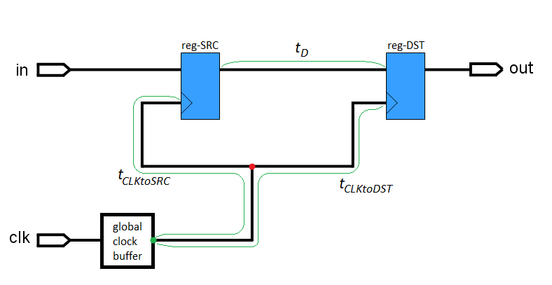
Fig. 3. Designation of the travel time of the paths of clock signals and data.
In this picture, we see two points - green and red. Both of them are points at which the paths of the source chunk and the destination chunk have not yet diverged. The green point is the output of the global clock buffer, the entry point to the global clock network of the FPGA, relative to which the clock inputs of all registers are approximately equidistant. The red dot is some arbitrary point in the global clock network, in which, like at the input of the network, the clock has not yet split into two copies of itself, which have gone to different registers. But only the green point is a suitable point to start counting the times for the passage of clocks, because it is in one of the places understandable by the compiler. In this example, at the input of the global clock network. But in the case of simple interfaces that are clocked from the outside, the green dot can be just an FPGA leg.The compiler knows the timings from this point to each of the registers. And the red dot, the place where the paths of the two analyzed clocks accidentally coincide, is not suitable for the starting point.
Types of analyzed transmissions
Let's classify cases for temporal analysis. The analysis is carried out separately for each FPGA leg with respect to a certain block. As a result of the analysis, the ability of the leg to correctly send or receive data is assessed. The external interface for synchronous data exchange between the FPGA and an external device consists of several lines connected to the legs. Of these, one line is the shred line. It must be shared between registers on both sides. The remaining lines, one or many, are unidirectional input or output lines. What is an input line for an FPGA is an output line for an external device, and vice versa. In this article, we consider only the simplest cases of temporal analysis, so we do not touch upon asynchronous and self-timed interfaces, as well as the use of bidirectional I / O lines.
Analysis cases can be classified according to the direction of data relative to the FPGA (Input / Output) and the direction of the clock relative to the FPGA (data is clocked from the FPGA / from an external source). For each case, there are two types of analysis (Setup / Hold). In total, four cases for analysis and eight equations that we need to derive.
Outputting data clocked by an internal FPGA clock
Consider the case when we need to give something out on our shred (Fig. 4).
The basic data transfer scheme has not changed. But the registers now belong to two different microcircuits, and the data path between them is not combinational logic, but just tracks on the board. And our task is to adapt the known slack formulas to a slightly different situation.
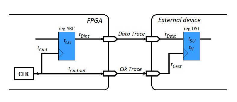
Figure: 4. Transferring data outward on your own FPGA clock.
In Figure 4, we see an inter-register transfer scheme. It shows the times of the processes associated with each of the registers, and the times for which signals travel the paths.
I set the following indexing: the time referring to the data is marked with the letter D. The time referring to the clock is marked with the letter C. If an event occurs inside the FPGA, then its time is marked with an "int" index, and if in an external device, then "ext" ... The time taken for the chunk to travel from the chunk source to the chunk exit stem has the longest index "Cintout". DataTrace and ClkTrace are the travel times of the corresponding traces on the PCB. The "CLK" block symbolizes a kind of internal source of clocks.
The main feature of the quantities mentioned in the figure is that they are all positive. All of them are equal to the absolute duration of any physical processes, which means that physically they can only be positive values. This is important for further reasoning.
Now we will take a closer look at the analysis of the preset slack. Looking at Figure 4, we can easily correlate the observed values with the terms of the slack formulas:
Now let's substitute these equalities into the preset slack formula:tCLKtoSRC=tCint
tD=tDint+DataTrace+tDext
tCLKtoDST=tCintout+ClkTrace+tCext
minSetupSlack=minDataRequired-maxDataArrival=
=SR+mintCLKtoDST-maxtCLKtoSRC-maxtSU-maxtCO-maxtD=
=SR+min(tCintout+ClkTrace+tCext)-max(tCint)-tSU-tCO-
-max(tDint+DataTrace+tDext)
Now we are using the knowledge that all the terms in parentheses are greater than zero. So we know how to open such brackets: the minimum of the sum is equal to the sum of the minimums, and the maximum of the sum is equal to the sum of the maxima:
minSetupSlack=SR+mintCintout+minClkTrace+mintCext-maxtCint-
-tSU-tCO-maxtDint-maxDataTrace-maxtDext
Now let's rearrange the terms in places so as to group the terms of processes inside the FPGA and processes inside the external device in brackets:
minSetupSlack=SR-(maxtCint+tCO+maxtDint-mintCintout)+
+minClkTrace-maxDataTrace-(maxtDext+tSU-mintCext)
What do we see in brackets? If you look closely and once again remember that all the indicated values are greater than zero, then we can say that we see an expression of a certain equivalent (with an asterisk) response time of the FPGA register and the equivalent presetting time of the external device register:
maxtCint+tCO+maxtDint-mintCintout=maxt∗CO
maxtDext+tSU-mintCext=maxt∗SU
minSetupSlack=SR-maxt∗CO+minClkTrace-maxDataTrace-maxt∗SU
Why don't we use equivalent values if the chip manufacturers have already calculated them for us, taking into account their internal delays? Equivalent values on the FPGA side will be calculated by the compiler without user intervention, and the equivalent values of the external device are explicitly indicated in the datasheet for the device.
Now let's take a closer look at the last expression. In it, the first three terms are already known to the analyzer, because we have already indicated to it the operating frequency and the magnitude of the instability. The compiler has traced and the analyzer knows the equivalent response time of its register. This means that the analyzer knows the duration of all processes inside the FPGA. But the last three terms are unique for each leg and the user needs to calculate them himself and indicate to the analyzer as a number. What is this number? Taking a closer look at the last three terms, we will see that they can be interpreted as a negative maximum of a certain value:
minClkTrace-maxDataTrace-maxt∗SU=-maxOutputDelay
And this value is meaningfully equal to the delay of everything that happens outside the FPGA, relative to everything that happens inside. It is called that - the output delay, Output Delay.
Let's summarize:
minSetupSlack=SR-maxt∗CO-maxOutputDelay
maxOutputDelay=maxDataTrace+maxt∗SU-minClkTrace=
=max(DataTrace+t∗SU-ClkTrace)
Now we will derive a similar equation for the retention slack. Recall the general equation and substitute new terms into it:
Let's open the brackets and immediately group the terms around each of the registers:minHoldSlack=minDataArrival-maxDataRequired=
=-HR+mintCLKtoSRC-maxtCLKtoDST+mintCO-maxtH+mintD=
=-HR+min(tCint)-max(tCintout+ClkTrace+tCext)+tCO-tH+
+min(tDint+DataTrace+tDext)
And again we see how the terms are grouped into equivalent quantities, this time tCO and tH:minHoldSlack=-HR+(tCO+mintCint+mintDint-maxtCintout)-
-maxClkTrace+minDataTrace-(tH-mintDext+maxtCext)
And the last three terms can be understood as the minimum external delay:minHoldSlack=-HR+mint∗CO+minDataTrace-maxClkTrace-maxt∗H
minDataTrace-maxClkTrace-maxt∗H=minOutputDelay
Let's summarize:
minHoldSlack=-HR+mint∗CO+minOutputDelay
minOutputDelay=min(DataTrace-ClkTrace-t∗H)
It should be emphasized that minOutputDelay and maxOutputDelay- this is the minimum and maximum not absolutely the same value. Each preset analysis and retention analysis consider different situations and different external delays. This means that the terms, as can be seen from the formulas, are taken differently.
Outputting data clocked by an external clock
Now let's move on to the case when we need to give something to the outside, but according to a clock external to the FPGA (Fig. 5). In general, the clock source is located outside the FPGA, in particular, it can be inside an external device.
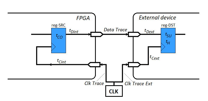
Figure: 5. Transferring data to the outside via an external clock.
In Figure 5, we see the source of the shred outside. Accordingly, the quantitytCintoutand the time for the passage of the chunk to the external device "Clk Trace Ext" appeared.
Looking at Figure 5, we correlate the observed values with the terms of the general slack formulas:
tCLKtoSRC=ClkTrace+tCint
tD=tDint+DataTrace+tDext
tCLKtoDST=ClkTraceExt+tCext
Using these expressions, we open the terms in the preset slack formula, immediately group them by registers and get the equivalent form:
minSetupSlack=minDataRequired-maxDataArrival=
=SR+mintCLKtoDST-maxtCLKtoSRC-maxtSU-maxtCO-maxtD=
=SR-(maxtCint+tCO+maxtDint)-maxDataTrace-
-(maxtDext+tSU-mintCext)-maxClkTrace+minClkTraceExt=
=SR-maxt∗CO-max(t∗SU+DataTrace+ClkTrace-ClkTraceExt)
minSetupSlack=SR-maxt∗CO-maxOutputDelay
maxOutputDelay=max(t∗SU+DataTrace+ClkTrace-ClkTraceExt)
We parse the retention slack in the same way:
minHoldSlack=minDataArrival-maxDataRequired=
=-HR+mintCLKtoSRC-maxtCLKtoDST+mintCO-maxtH+mintD=
=-HR+(mintCint+tCO+mintDint)+minDataTrace+minClkTrace-
-(tH-mintDext+maxtCext)-maxClkTraceExt=
=-HR+mint∗CO+minDataTrace+minClkTrace-maxClkTraceExt-maxt∗H
minHoldSlack=-HR+mint∗CO+minOutputDelay
minOutputDelay=min(DataTrace+ClkTrace-ClkTraceExt-t∗H)
If in this scheme we consider a particular (but frequent) case when the source of the trick is inside an external device, then the derived formulas will change only by the fact that ClkTraceExt becomes equal to zero in them. Moving the source of the clock to the inside of the external device will cause in our calculations microscopic spreading of the clot inside the external device between the clock output and the register, but it will be taken into account by the manufacturer of the external device and will be included in the values equivalentt∗SU and t∗H...
Input of data clocked by an internal FPGA clock
We now turn to consideration of the input legs of the synchronous interface. The FPGA and the external device in Figure 6 are swapped.
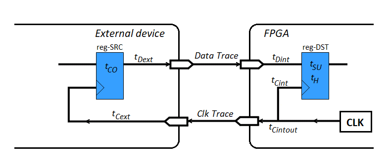
Figure: 6. Receiving data on your own FPGA clock.
The analysis of such a scheme is no more complicated than the previous ones.
We reveal, we group ...tCLKtoSRC=tCintout+ClkTrace+tCext
tD=tDext+DataTrace+tDint
tCLKtoDST=tCint
And we get the value of the external delay, which this time we will call the input:minSetupSlack=minDataRequired-maxDataArrival=
=SR+mintCLKtoDST-maxtCLKtoSRC-maxtSU-maxtCO-maxtD=
=SR-(tSU+maxtDint-mintCint+maxtCintout)-maxDataTrace-
-(tCO+maxtDext+maxtCext)-maxClkTrace
minSetupSlack=SR-maxt∗SU-maxInputDelay
maxInputDelay=max(DataTrace+t∗CO+ClkTrace)
Now the hold slack:
minHoldSlack=minDataArrival-maxDataRequired=
=-HR+mintCLKtoSRC-maxtCLKtoDST+mintCO-maxtH+mintD=
=-HR-(tH-mintDint+maxtCint-mintCintout)+minDataTrace+
+(tCO+mintDext+mintCext)+minClkTrace
minHoldSlack=HR-maxt∗H+minInputDelay
minInputDelay=min(t∗CO+DataTrace+ClkTrace)
Entering data clocked by an external clock
Also, according to the knurled one, we look at the data transfer scheme and reveal the terms of the general formula.
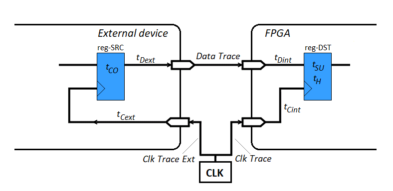
Figure: 7. Reception of data on external clocks.
tCLKtoSRC=ClkTraceExt+tCext
tD=tDext+DataTrace+tDint
tCLKtoDST=ClkTrace+tCint
Preset slack formula:
minSetupSlack=minDataRequired-maxDataArrival=
=SR+mintCLKtoDST-maxtCLKtoSRC-maxtSU-maxtCO-maxtD=
=SR-(tSU+maxtDint-mintCint)-maxDataTrace-
-(tCO+maxtDext+maxtCext)-maxClkTraceExt+minClkTrace=
=SR-maxt∗SU-max(t∗CO+DataTrace+ClkTraceExt-ClkTrace)
minSetupSlack=SR-maxt∗SU-maxInputDelay
maxInputDelay=max(t∗CO+DataTrace+ClkTraceExt-ClkTrace)
Slack retention formula:
minHoldSlack=minDataArrival-maxDataRequired=
=-HR+mintCLKtoSRC-maxtCLKtoDST+mintCO-maxtH+mintD=
=-HR-(tH-mintDint+maxtCint)+minDataTrace+
+(tCO+mintDext+mintCext)+minClkTraceExt-maxClkTrace
minHoldSlack=-HR-maxt∗H+minInputDelay
minInputDelay=min(t∗CO+DataTrace+ClkTraceExt-ClkTrace)
Again, if the source of the clock is inside an external device, then simply equate ClkTraceExt to zero.
Visual interpretation
Formulas are certainly good, but if you dive into this topic for the first time, the formulas look incomprehensible, lifeless. I would like something clearer so that the formulas gain visible meaning. Okay, let's analyze the physical meaning of the formulas, taking, for example, the case of outputting data by an external clock . Let me remind you how the diagram and formulas look like:

Fig. 8. Transfer of data to the outside via an external clock.
minSetupSlack=minDataRequired-maxDataArrival=
=SR-maxt∗CO-maxt∗SU-maxDataTrace-maxClkTrace+minClkTraceExt
minHoldSlack=minDataArrival-maxDataRequired=
=-HR+mint∗CO+minDataTrace+minClkTrace-maxClkTraceExt-maxt∗H
During the transfer of data, two events occur: the source register fires and the destination register fires. Events happen because they are triggered by the clok fronts emerging from the cloc source. From here we will start looking.
The source of the clock generates a start-up front and it gets to the FPGA during ClkTrace. Next, the FPGA register is triggered duringt∗CO... Further, the new data generated by this trigger goes from the FPGA to the external device during the DataTrace.
On the other hand, the source of the clock also generates the capture front, which gets to the external device during ClkTraceExt.
These two events occur at the data input of an external device. And here it is important that the data arrives there before the receiving register starts capturing. They should come with at least some time left.t∗SU, or better yet. The worst case is considered to ensure this is true. If there is a reserve even in the worst case, then everything is definitely in order. Therefore, the worst moment of data arrival is the latest moment,max(ClkTrace+t∗CO+DataTrace)... And the worst moment of waiting for data is the earliest moment,minClkTraceExt-maxt∗SU... And even in the worst case, the second moment should be later than the first:
Hopefully this explanation sheds more light on what's going on.LatchEdge+minClkTraceExt-maxt∗SU>
>LaunchEdge+max(ClkTrace+t∗CO+DataTrace)
In this expression, we see the moments of the fronts - LaunchEdge and LatchEdge, which are usually hidden in the SR and HR terms. Let's remember what it is. Four edges are considered in the preset and hold analysis:
Setup Launch Edge is the edge that will cause the source to send data that the receiver should catch.
Hold Launch Edge is the front that will force the source to send the next data, which can prevent the recipient from grabbing the previous ones. By definition, there is always one clock period between Setup LaunchEdge and Hold Launch Edge.
The Setup Latch Edge is the front that will force the receiver to capture input data.
Hold Latch Edge is the same Setup Latch Edge. That is, in fact, Latch Edge is physically one, it is simply given two names for beauty in two types of analysis.
Within FPGAs, synchronous logic usually only works on rising edges (Figure 9). In this case, from the point of view of the slack analysis, the Setup Launch Edge and Setup Latch Edge presets are spaced from each other by one clock period, and from the point of view of the analysis of holding, Hold Launch Edge and Hold Latch Edge coincide.

Figure: 9. Mutual arrangement of the edges in the case when both registers are clocked by the rising edges.
However, no one forbids putting an inverted clock signal on the clock input of one of the two registers and thereby making it work on the falling edge of the clock. This, by the way, is often done in the same SPI interfaces. Let's take a closer look at this option.
Consider the situation of data output from the FPGA by an external clock, but one of the two registers operates on an inverted clock, that is, along a falling edge. Let it be a receive register on an external device. Then the roles of the fronts in time will be distributed differently (Fig. 10).

Figure: 10. Mutual arrangement of fronts in the case when the source is clocked by the rising edge, and the receiver by the falling edge.
This inclusion of registers allows you to align the size of the slacks for preset and hold. If the registers worked from the fronts of the same direction, then because of the scanty, in comparison with the period of the clock, the propagation of signals along the board tracks, the preset slack would be huge, and the hold slack would be very small.
Figure 11 shows the timing versus clock at the clock source. To simplify the figure, I did not specify the ClkTraceExt term. We will assume that the source of the shred is inside an external device.

Figure: 11. The position of the slacks in time relative to the clocks fronts in the case when the receiver is clocked by the falling edge.
In this picture, max Data Arrival- this is the latest moment when data can arrive at the receiver's input. The earliest moment when the data should already be at the receiver's input is min Data Required . The latest moment when data still needs to be at the receiver's input is max Data Required . And the earliest moment when data can already leave the recipient's input, being replaced by the next data, is called min Data Leaving .
Now the formulas and their terms should become clearer.
How to use the resulting formulas
We have obtained formulas for external delays and can calculate specific numbers of delays to fit them into the time constraints file. Globally, these formulas consist of two types of terms - the timing characteristics of the ports of the external device and the latency on the board tracks.
Port specifications are usually found in datasheets under sections titled like "Electrical Characteristics / AC Specifications / Timing Requirements". Sometimes these characteristics are called by different names and you have to be smart to find them. But tables with numbers are usually accompanied by timing charts that will allow you to identify the parameter you want. An important nuance, which can be confusing, in datasheets for many microcircuits, output pins are often described by the "Setup Output time" and "Hold Output time" parameters. In the formulas of this article, they should be compared as follows:tSUO=maxt∗CO,tHO=mint∗CO...
With tracks, it's a little more complicated. Exact calculation of the latency on the board is not a trivial question. The delay depends on the length, width, thickness and angles of the track, the thickness and material of the board, the distance to different ground layers, the proximity of the tracks to each other and many other factors. However, the influence of each of these factors is rather small and at low interface frequencies, up to tens of megahertz, these difficulties can be neglected. A simplified calculation of the delay on the track looks like this: the speed of propagation of the wave in the foil is considered equal to half the speed of light in vacuum. When converted, this gives approximately 0.007 ns / mm. The error in this estimate is offset by a wide range of delay estimates. For the maximum delay, we consider the specific delay equal to 0.010 ns / mm, and for the minimum - 0.005 ns / mm.
There is one more nuance. Circuit engineers, when designing printed circuit boards, try to stretch the tracks of synchronous interfaces in approximately the same way and keep their equal lengths. Check the data and clock track lengths on your target board. Most likely they are almost equal and the component of expressions (DataTrace - ClkTrace) in practice can be considered null.
If there is a delay element in the path of the data or chunk, it must also be taken into account. It can be a buffer, inverter, level converter or galvanic isolation. Such elements are capable of introducing a very large delay, tens of nanoseconds, so they need to be treated very carefully.
Conclusion
In this article, you saw the formulas that determine the execution of time constraints in synchronous interfaces. Knowing these formulas, you can understand what the successful data transfer depends on and how to calculate the correct limits for the analyzer. In the next article I will give an example of formatting a time constraint file and using the analyzer.