It is noteworthy that MOS structures still work, being greatly reduced, while most things cannot just be reduced like that. For example, you cannot scale a motor 10 times and expect it to work. Most physical objects suffer from the square-cube law : the area of an object grows as a square of linear size, and its volume as a cube. However, in the case of MOS structures, most of the components when scaling either remain unchanged or improve (for example, frequency and power consumption). For more details on scaling, see Mead and Conway's book Introduction to VLSI Systems.... Ironically, the 1978 book claims that scaling has a fundamental quarter-micron (250 nm) limitation on channel length due to the physical properties of matter. This limitation turned out to be incredibly flawed - now transistors are moving to the characteristic size of 5 nm, thanks to technologies such as FinFET.
The photo below shows the 8086 chip from 1979, as well as its version with a clearly smaller die from 1986. The ceramic covers have been removed from the chips so that the crystals can be seen. In the updated 8086, the internal circuits have been reduced by 64% in length compared to the original, so it occupies 40% of the original area. The crystal itself is not greatly reduced; it occupies 54% of the original area. Processor housing is not changed, the DIP 40-pin while often used for microprocessors.
The old chip says '78, '79 on the case and 1979 on the crystal, and the date code is 7947 (47th week of 1979) at the bottom. 1978 is written on the case of the new chip, and 1986 is written on the crystal, there is no date code. Therefore, it should be manufactured in 1986 or a little later. It is not clear why the new chip on the case has an older date.
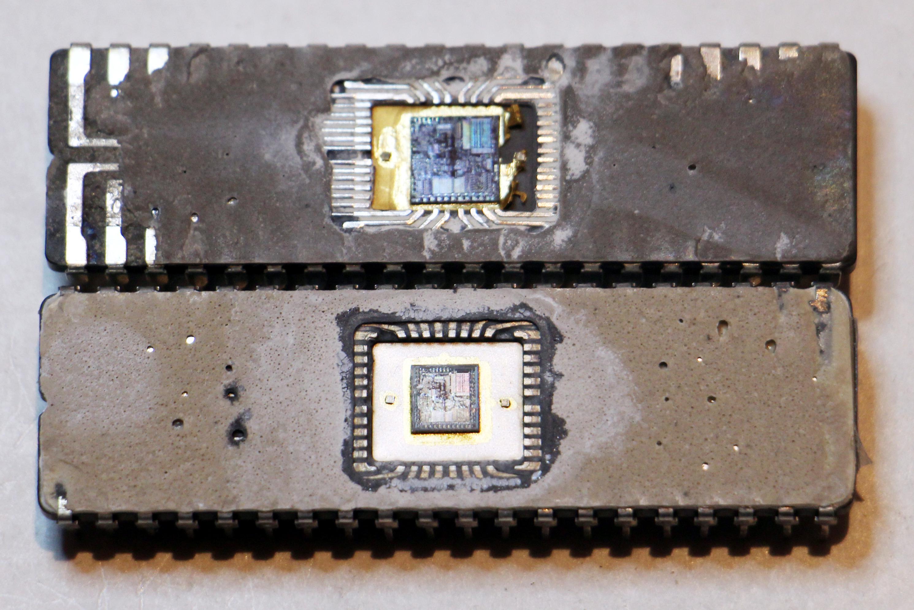
Comparison of two 8086 chips. The bottom of the new chip has a much smaller die. The rectangle in the upper right corner is the microcode ROM.
The 8086 is one of the most influential chips ever made. He laid the foundation for the x86 architecture that still dominates both desktop and server computers. Unlike modern CMOS processors, the 8086 was built on N-MOS transistors like the 6502, Z-80, and other early processors. The first chip was made using HMOS technology, as Intel called this process. In 79, Intel introduced an advanced version of it, HMOS-II, and in 82 it switched to HMOS-III, the process used to make the newer of my two chips. Each successive version of HMOS shrinks the size of the chip components and increases efficiency.
An N-channel MOSFET is a specific type of MOSFET. Their efficiency is much better than that of the P-channel MOS structure used in early microprocessors such as the Intel 4004. Modern processors use N-channel and P-channel transistors together to reduce power consumption - this is called CMOS... Gates made from N-channel MOSFETs require a pull-up resistor, which is a transistor. Depletion load transistors are a type of transistor introduced in the mid 1970s. Transistors of this type are better suited for the role of pull-up resistors and do not need additional supply voltage. Finally, MOSFETs originally used metal to create gates (the letter M in MOSFETs). However, in the late 1960s, Fairchild developed polysilicon to replace metal. As a result, the chips are more efficient and easier to manufacture. As a result, from the late 1960s to the mid 1970s, several radical changes occurred in the production of MOS structures, leading to the success of the 6502, Z-80, 8085, 8086 and other early processors. In the 1980s, CMOS processors took over because they were faster and consumed less power.
Strangely, what exactly the H in the acronym HMOS stands for is not entirely clear. I have not found a transcript of this acronym from Intel. The spec says " Intel's advanced silicon N-channel HMOS gates manufacturing process," or "HMOS is a highly efficient n-channel MOS process." Intel later described CHMOS as Complementary High Speed Metal Oxide Semiconductor [complementary high speed metal oxide semiconductor]. Motorola has identified HMOS as High Density MOS. Other sources describe it as a high speed MOS or high density MOS with short channels. Intel has a patentto "MOS process and high density and high speed device", so perhaps H stands for both "high density" and "high speed".
Interestingly, Intel used 4K static RAM to develop each of the HMOS processes before using the process for microprocessors and other chips. She used a RAM chip, probably because it has very dense circuits, but it is also relatively easy to design, since the same memory cell is repeated over and over again. Once she had developed all the circuit layout rules, she was able to start building much more complex processors.
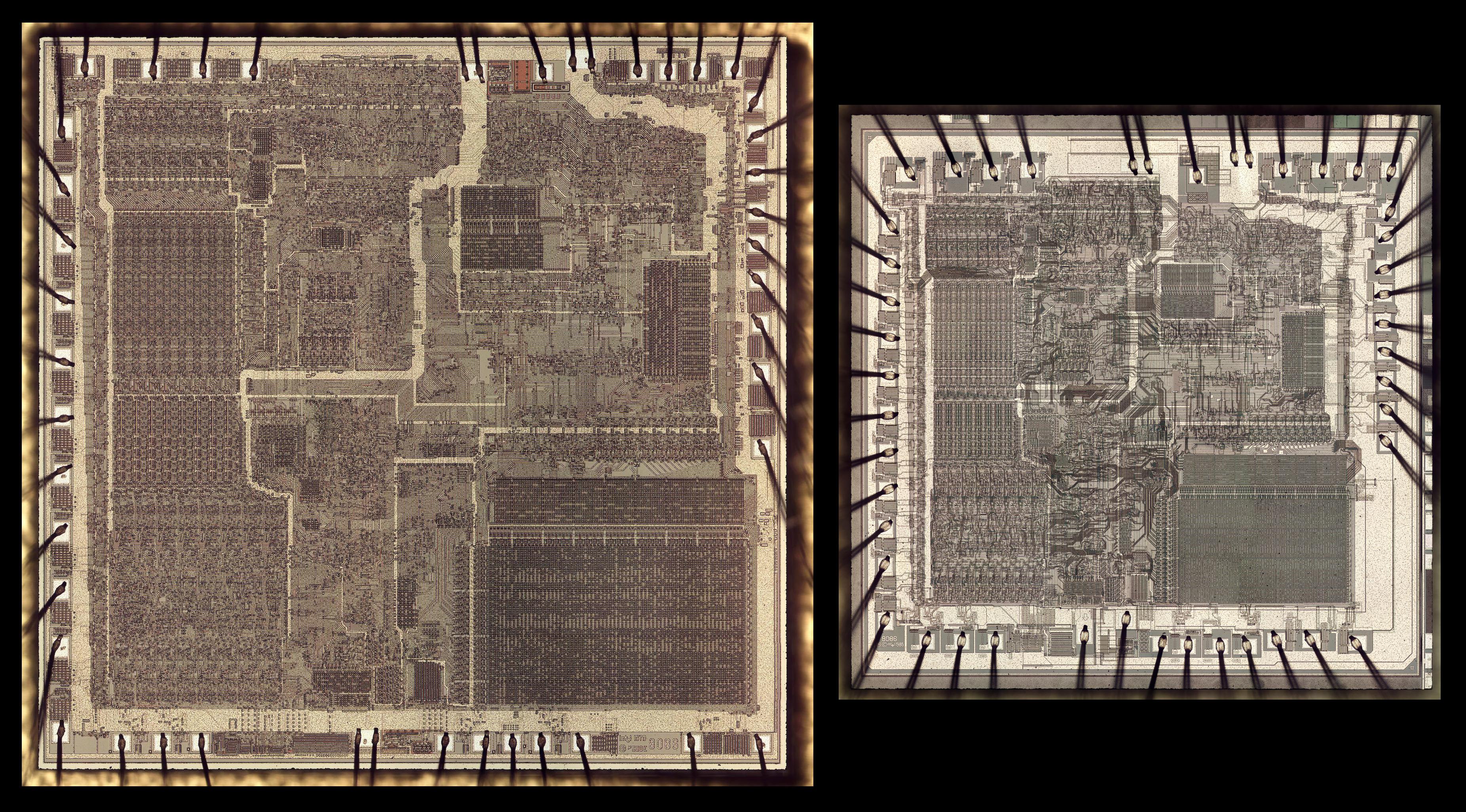
Two versions of the 8086 crystal at the same scale. Incoming conductors are connected to the pads located around the perimeter of the crystal.
The photo above shows two versions of the 8086 crystal at the same scale. The two chips have the same layout of the components inside, although at first glance they may seem different. The chip on the right in the middle has many dark lines that the chip on the left does not, but this is just a shooting artifact. These lines are a layer of polysilicon located under the metal. On the left side of the crystal, all the conductors are located in the same way, only in the photo they are very pale. I think that the new chip has a thinner metal layer, which is why polysilicon is seen better.
I scaled high-resolution photos of the two chips to compare them, and it turned out that the main parts of the chips are completely the same, except for some trivial differences. The only question is whether there were changes in the microcode. From the outside they look identical, but I did not compare them bit by bit.
The enlarged photo below shows the identical chains of two crystals. You can see the exact correspondence between the components, which proves that the circuit was only reduced in size, and not redone. In the photo, the metal layer is on top of the chip. The right photo shows some polysilicon.
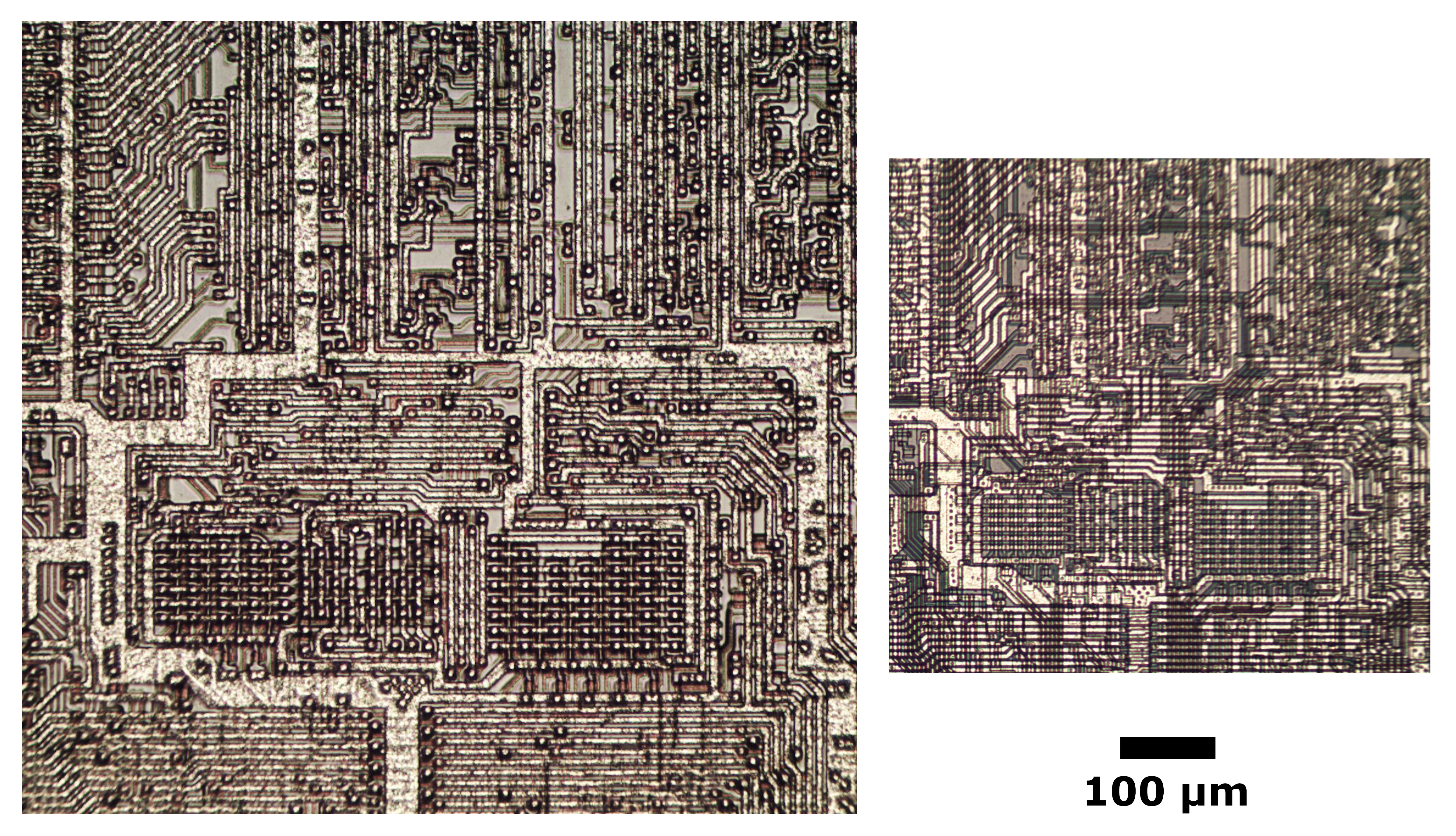
The same plot on two different chips, on the same scale
But along the perimeter of the crystals, the differences are significant. The contact pads are closer together, especially at the bottom right. There are two reasons for this. First, the contact pads cannot be significantly reduced, as they need to be attached with connecting wires. Second, the power distribution tracks are widened at the edges to maintain the required current. For example, look at the bottom right of the photo, to the right of the microcode RAM. In particular, this is because the power tracks in the middle of the circuit are scaled down along with everything else, so the outer tracks need to compensate for these losses. In addition, the thinner metal layer in the new chip cannot support the same current unless it is expanded.
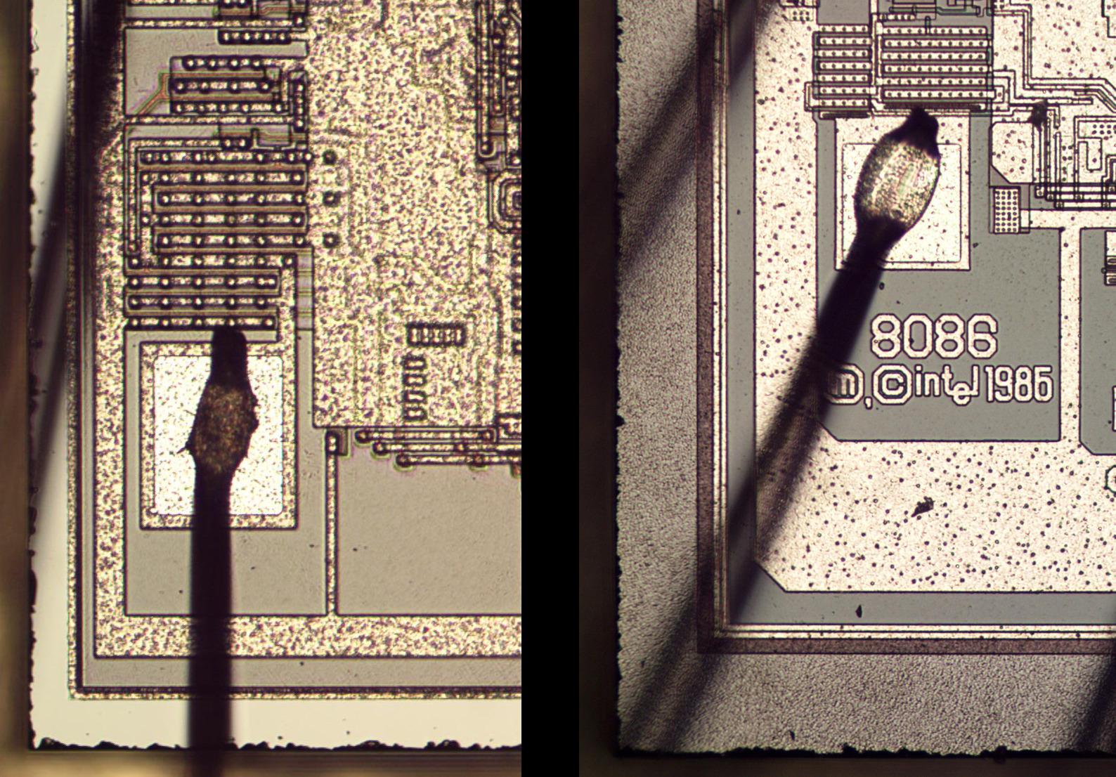
Contact pad and accompanying transistors on the old chip (left) and new (right). The number "6" in the copyright date has an unusually flat top - it looks like it is "5" corrected to "6".
The photo above shows a pad with a soldered jumper wire. The transistors are located above the pad. The site of the new chip is almost the same size, but the transistors are downsized and redesigned. Note the much thicker metal conductors on the new chip. The Intel logo was moved from right to left, possibly because there was free space.
Let's take a closer look at the crystals
First, a little history of the production of n-channel MOSs used in the 8086 and other chips from that era. These chips consisted of a silicon substrate to which arsenic or boron impurities were added to form transistors. The layer of polysilicon on top creates gates for the transistors and makes it possible to connect components with conductors. Finally, one metal layer at the top binds all the components together.
The semiconductor manufacturing process (for example, HMOS-III) has certain rules for the minimum size and distance between components - silicon, polysilicon and metal layers. If you take a closer look at the chips, you will see how these parameters were different for HMOS I and HMOS III. The plate (taken from the HMOS III Technology) summarized the characteristics of various HMOS processes. With each version, the characteristic size decreased, and the performance increased. In moving from HMOS-II to HMOS-III, Intel achieved a performance improvement of 40%.
| HMOS I | HMOS II | HMOS III | |
|---|---|---|---|
| Diffusion step (µ) | 8.0 | 6.4 | 5.0 |
| Polysilicon pitch (µ) | 7.0 | 5.6 | 4.0 |
| Metal step (µ) | 11.0 | 8.0 | 6.4 |
| Valve oxide thickness (Å) | 700 | 400 | 250 |
| Channel length (µ) | 3.0 | 2.0 | 1.5 |
| Idsat (mA) | 8.0 | 14.0 | 27.0 |
| Minimum valve delay (ps) | 1000 | 400 | 200 |
| Heat dissipation valve delay (pJ) | 1.0 | 0.5 | 0.25 |
| Linear reduction rate | 1.0 | 0.8 | 0.64 |
The photo below, taken through a microscope, shows the complex arrangement of transistors in the old 8086 chip. Dark areas are silicon with impurities, light rectangles are transistor gates. The photo shows about 21 transistors. The key dimension is the channel length, the length of the valve from source to drain (this is the smaller side of the light rectangles). For these I measured a length of 3 µm, which is in line with the published specifications of HMOS I. This suggests that the chip was manufactured using the 3 µm process technology; for comparison, today processors are switching to 5 nm, which is 600 times smaller.
You may have noticed that the three transistors in the photo have much larger gates. These transistors operate as pull-up resistors, which is typical of NMOS. Increasing their size weakens the transistor, so the pull-up current is weak.

8086. . – , .
The photo below shows the transistors in the newer 8086 at the same scale; you can see that the transistors are already much smaller in size. The linear dimensions are 64% of the original, so the transistors occupy 40% of the area compared to the previous ones. I processed this crystal in a different way, so polysilicon remained on it - these are yellowish lines. Silicon with impurities looks pinkish, and it is less visible than in the previous photo. I determined the valve length to be 1.9 microns, which is 64% of the previous 3 microns. Note that the HMOS-III maintains a significantly shorter channel length of 1.5 µm, however, since everything is reduced by the same number of times, the channel length is longer than necessary. This shows that a uniform decrease leads to the loss of certain advantages of the new process, but this is much easier to do.than designing a new chip from scratch.

The transistors in the new 8086 chip. There are many through conductors between silicon or polysilicon and the metal layer (removed here).
I also studied the pitch between the tires on the metal layer. The photo below shows the horizontal and vertical metal conductors of the old chip. I determined the pitch of the metal tires at 11 microns, which coincides with the published characteristics of HMOS I. Reducing to 64% gives a step of 7 microns on the new chip, although the HMOS III process also supported 6.4 microns. As before, the same reduction factor prevents you from enjoying all the benefits of the new process.

The metal layer of the old 8086 chip. Reddish polysilicon conductors are visible under the metal.
Finally, I studied the pitch of the polysilicon conductors. The photo below shows the old 8086; the polysilicon has been removed and only faint white lines are visible. These parallel polysilicon lines likely formed a bus that sent signals from one part of the chip to another. For polysilicon, I measured a step of 7 microns, which matches the documentation. Interestingly, due to the properties of HMOS, polysilicon conductors can be packed closer together than metallic conductors. The new chip has a pitch of 4.5 microns, although it is possible to make it 4 microns in size.
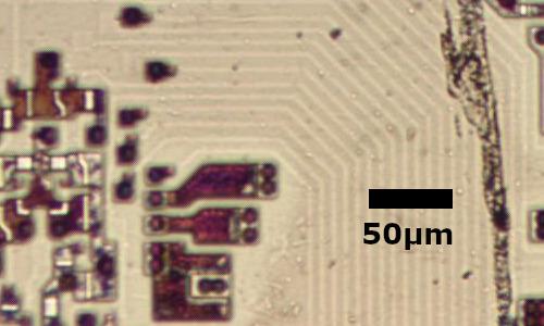
Polysilicon tracks on the old 8086 chip
Conclusions.
Scaling the crystal makes it possible to increase the speed of the processor and reduce its cost, without wasting efforts on designing from scratch. However, a comparison of the two chips shows that scaling a die is a more complex process than simply shrinking the entire die. Most of the circuit just shrinks, but the pads don't shrink as much as the rest, so they have to be rearranged. The power distribution has also been changed, and more power conductors have been added around the chip.
Modern microprocessors still use crystal scaling technology. In 2007, Intel switched to a tick-tock model, in which the scaling of existing chips ("tick") alternates with the release of a new microarchitecture ("tock").
See also: