The lidar-equipped Apple iPad 11 Pro has deeper and more detailed recognition of 3D objects. For this, ToF cameras are also used with different technologies for measuring the range of the point position.
Apple has pioneered a race to use lidars across a variety of products. Apple has built lidar into its iPad Pro 11, and now it seems like everyone wants to use lidar.
Apple's maneuver and reaction to it have impacted the entire electronics industry. Chip and sensor vendors are reconsidering their plans. Some have already changed their business models.
But what is lidar? Apple chose this term to describe a new sensor that measures depth — in other words, a sensor that recognizes objects in three dimensions.
The lidar in tablets and smartphones is essentially “just a kind of technology for recognizing three-dimensional objects,” explained Pierre Cambu, chief analyst for the company's photonics and display department at Yole Développement.
Many engineers in various fields - be they self-driving cars, smartphones or tablets - have explored ways to use the "depth" information of the data in conjunction with the pixels and colors obtained from sensors that recognize two-dimensional objects. For example, lidars are used in the automotive industry to determine distances to objects located around highly automated vehicles.
Apple's recently unveiled iPad 11 Pro uses lidar to enhance its augmented reality experience. This lidar is designed for Apple's ARkit 3.5 development kit.
The special technology used to determine and measure depth makes this lidar essential. It is this technology that has caused this sensor to be monitored by other mobile device manufacturers, including Huawei and Vivo.
Different methods of recognition of three-dimensional objects
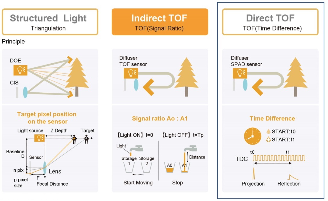
Engineers use a variety of techniques to recognize 3D objects . These include stereo vision, light structuring and time-of-flight (ToF) measurements. To complicate matters further, ToF technology is now available in two versions: iToF and dToF. iToF measures the phase shift and dToF measures the direct flight time.
The Apple iPhone X features structured light facial recognition. Its depth estimation works with an IR emitter that sends out 30,000 points in a fixed order. The dots are invisible to humans, but not to the IR camera, which reads deformations in the template that reflect off surfaces at different depths.
With the release of iPad 11 Pro, 3D object recognition has become deeper and more detailed thanks to the use of dToF technology. Apple's iPad Pro is the only consumer product to date using dToF technology. Many smartphone manufacturers already use iToF for better photos (ToF camera can blur the background in photos), but not dToF.
The lighting structuring method provides high accuracy in determining the depth, but its disadvantage is the complex post-processing required for calculating the depth when matching with the sample.
The advantage of the dToF method, by contrast, is its ability to provide ease of post-processing. However, it is believed that the difficulty of using this technology lies in the fact that photodetectors with high sensitivity (for example, single-photon avalanche photodiodes) and large size are required to measure flight time with a small number of photons in one dimension.
Currently, iToF is the most common 3D object recognition method. It provides highly accurate depth sensing, easy post-processing and high spatial resolution using small-sized photo detectors commonly used in 2D imaging sensors.
However, Apple has taken a less beaten path to recognize 3D objects. The company decided to use structured light to identify faces. For augmented reality, Apple uses dToF.
So, here are the questions that everyone in the world of 3D object recognition is asking: What is dToF? What is this technology made of? And who developed its components?
Analysis from System Plus Consulting, a division of Yole Développement, presented the details of the 3D object recognition module in the Apple iPad 11 Pro.
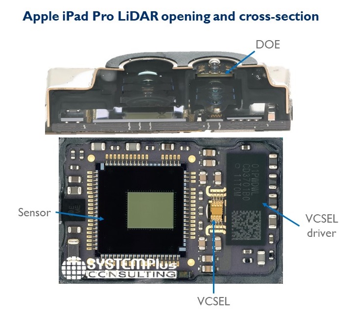
In an interview with the EE Times, Sylvain Hallero, senior technology and value analyst at System Plus, explained that the iPad 11 Pro's lidar consists of a vertical emitting laser (VCSEL) from Lumentum and a Sony-developed receiver, a near-field CMOS sensor. infrared range (NIR), which measures flight time.
Near-infrared CMOS sensor using Sony single-photon avalanche photodiodes
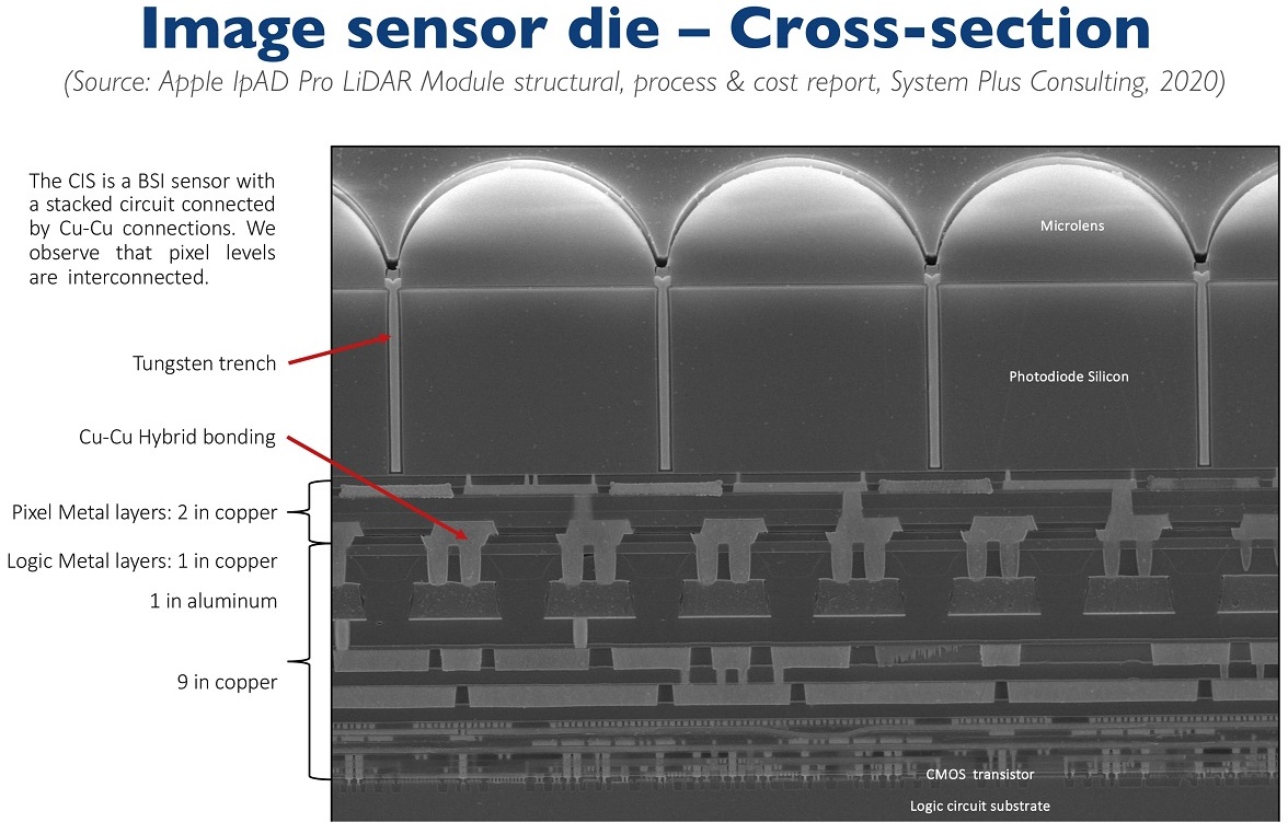
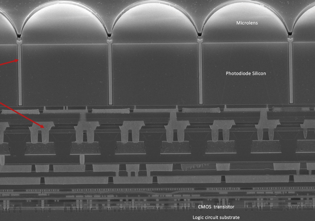
A cutaway from Sony's CMOS sensor, as part of a study of its device, was a revelation to experts following the development of photonics. Including for Kambu, who works for Yole. In a recent blog post , he wrote that what "looked like an old device with iToF and 10-micron pixels" turned out to be the first consumer CMOS sensor with an intra-pixel connection - and, yes, we are talking about an array of single-photon avalanche diodes. "
Intra-pixel connection is an important property. Sony is the first to integrate a CMOS sensor using 3D stacking for ToF sensors. The intra-pixel connection allowed the CMOS image sensor to be placed together with the logic substrate. Thanks to the integrated logic array, the sensor can make simple calculations of the distance between the iPad and objects, Hallero explained.
Sony has made its way into the dToF segment with the development of a new generation of CMOS sensors with 10-micron-pixel, 30-kilopixel single-photon avalanche diode arrays.
This isn't just a technological feat of Sony, though. It is also about the fact that Sony has changed the concept of its business.
Traditionally, the Japanese giant has worked more on image processing. not over scanning. However, Kambu states that "Sony renamed its semiconductor division a year ago to be called Imaging and Scanning." Next, Sony has taken two steps. The first was the delivery of iToF sensors to Huawei and Samsung in 2019, which earned Sony about $ 300 million. The second step is winning the competition for the development of dToF sensors for the Apple iPad. "
Kambu suspects that dToF sensors could eventually enter the iPhone. In his analysis, he notes that “Sony's sensor revenues are likely to surpass $ 1 billion in 2020 in a market that has just surpassed the $ 10 billion mark. This successful transition from image processing to scanning has played an important role in Sony's continued strength in the CMOS sensor market. All this will be the basis for the prosperity of the new division. "
Lumentum vertical emitting lasers
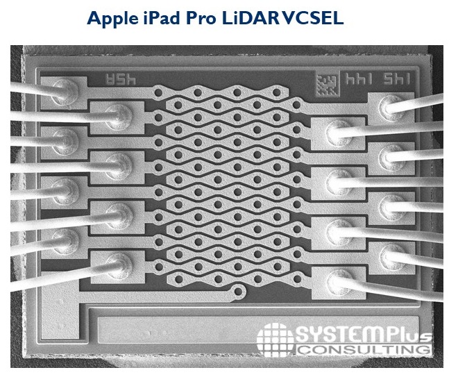
In addition to Sony's CMOS sensor, the lidar is equipped with vertical emitting lasers from Lumentum. In the design of these lasers there are several electrodes connected to the emitter.
Taha Ayari, Technology and Value Analyst at System Plus, has focused on a new processing step (called a mesa contact) that Lumentum has added to its vertical laser. A Lumentum laser emits light from the surface of the substrate. Fine tuning the emission requires power management and the application of various controls to the emitting arrays. Ayari believes Lumentum added this technology to improve component testing on substrates.
For pulse generation and power and beamform controlthe emitter uses an IC driver from Texas Instruments. The circuit uses a wafer-based package (WLCSP) molded on five sides.
Finally, System Plus claims that Lumentum's laser uses a new diffractive optical element (DOE) from Himax to create the dot pattern.
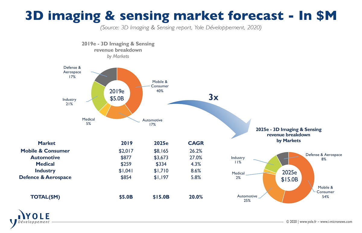
On the following pages, we share a few slides created by System Plus that illustrate what was found during the disassembly, and we also added a few slides describing the outlook for the lidar market.
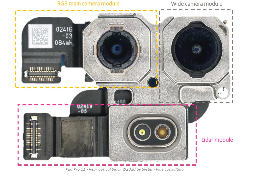
Apple iPad Pro features: RGB main camera module, wide camera module and rear LiDAR module
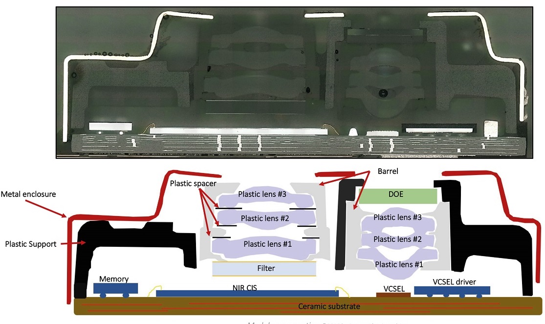
Here's how the cross section of the LiDAR module looks like.
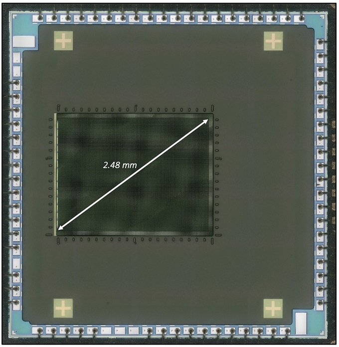
Image Sensor Overview
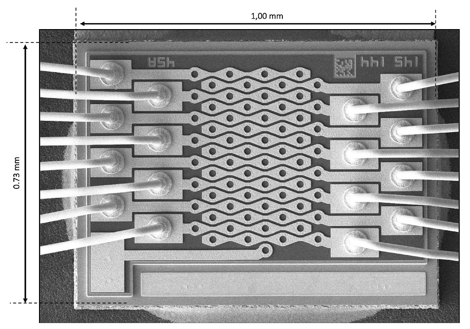
What VCSEL Die Looks like
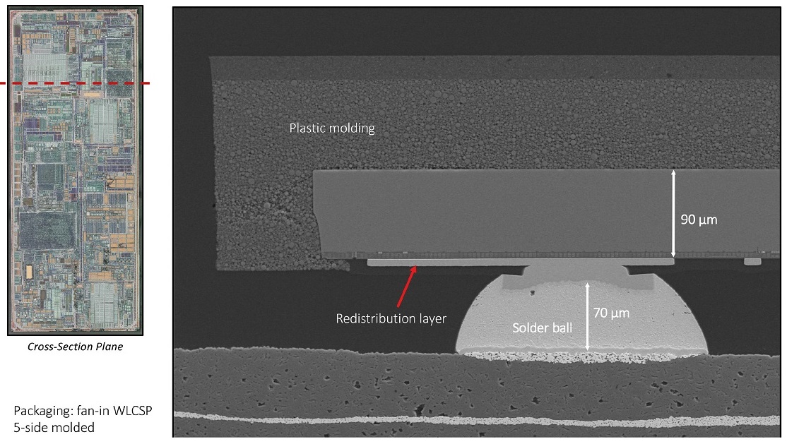
VCSEL Driver IC packaged in fan-in WLCSP 5-Side VCSEL Driver Die

Diffractive Optical Element
Subscribe to channels:
@TeslaHackers - a community of Russian Tesla hackers, rental and drift training on Tesla
@AutomotiveRu - auto industry news, hardware and driving psychology

About ITELMA
- automotive . 2500 , 650 .
, , . ( 30, ), -, -, - (DSP-) .
, . , , , . , automotive. , , .
, , . ( 30, ), -, -, - (DSP-) .
, . , , , . , automotive. , , .
Read more helpful articles:
- Free Online Courses in Automotive, Aerospace, Robotics and Engineering (50+)
- [Forecast] Transport of the future ( short-term , medium-term , long-term horizons)
- The best materials on hacking cars from DEF CON 2018-2019
- [Forecast] Motornet - data exchange network for robotic transport
- 16 , 8
- open source
- McKinsey: automotive
- …