The article was created on the basis of my own experience of attempts to explain this topic to myself, student-trainees and curious colleagues so as not to plunge into abstruse academic jungle, but as simply and transparently as possible, in everyday language. I learned to work with FPGAs without studying and training on this topic and I know from my own experience how difficult it is to understand something without a theoretical basis in this topic and in circuitry. For an experienced breeder, the above is elementary. But for some fourth-year student, the article will be useful and will help to understand all these slacks, setups and holds.
In the article, I will use terms with duplication of their English version in brackets. This is done because a unified terminology is not settled, and with duplication it is easier to understand what concept is being discussed and, if necessary, find information about it in English-language sources.
Introduction
I will give a short introduction in the language of simple concepts.
In order for something to work in the FPGA, you need to load (fill in, sew) the firmware file into it using the programmer and the firmware utility. The firmware file is the product of a CAD compilation of a certain project - folders with files, each of which describes some aspect of the project. In simple cases, the user himself describes only files with source code, a file with a pinout, and a file with time restrictions. The rest of the files are quietly handled by CAD. Of this triad, only the time constraint file is formally optional.part of the project. Actually, if your project does not contain frequencies higher than 30-50 MHz, then it is likely that it will be able to somehow work without this file. This option is appropriate for the ease of creating the very first educational projects. However, if your training project already contains high clock frequencies and is not equipped with a time constraint file, then most likely somewhere inside the FPGA, data processing will be disrupted, and you will not be able to find out at which point in the project. As for work, not study, the description of the full file of restrictions is strictly required . It is your responsibility to verify and validate the functionality of your project.
The compiler places your project on the FPGA chip, receives a file of connections of all physical elements. The timing analyzer uses the connection file to calculate all the durations of data transfers to the FPGA. These durations should not be infinitely long or too short. The file of time constraints tells the analyzer in what framework these durations should be. Using the results of time analysis, the developer can see in which parts of the project there is a margin in time, and therefore in frequency, and where there is no such margin.
Synchronous systems synchronize data processing work using synchronization clock signals, which in jargon are shortly referred to as clocks from the English clock... Intermediate results of operations are stored in registers capable of memorizing the state at the input at the moment of arrival of the clock signal edge and holding it at the output until the next clock cycle.
Thus, synchronous circuits consist of interregister data transfers ( RTL, register transfer logic, r2r transfer ). And a key aspect of temporal analysis consists in measuring Slack ( slack ). This word literally translates as "time reserve", "sagging", but in the Russian-speaking environment, tracing paper from English is often used - "slack". In interregister transfers, we are talking about preset slacks ( Setup ) and hold slacks ( Hold ).
Inter-register transfer
Interregister transfer (Fig. 1) is considered as a system of two sequentially connected registers that operate on synchronous clocks in the general case. In the simple case, on one shred. One register plays the role of the source (source), and the other role of the receiver of data (destination). And in the next inter-register transfer, this recipient register will already be considered as the source, etc. Between the registers on the data path is some arbitrary user-defined combinational logic. It is asynchronous since it does not have memory elements with a synchronizing signal, like registers. This logic is that behavior, those logical operations that the user describes with his code. Registers are those one-bit "variables" that the user gives names to in the code and operates separately,or combining into vectors and arrays.
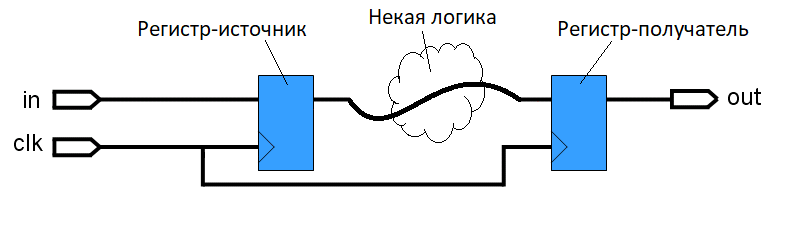
Figure: 1. Scheme of data transfer from register to register
There are two concepts associated with receiving data by the receiving register: Setup time and Hold time. They outline the range of time during which the signal at the receiver's input must be stable and relevant. Stable - essentially means that its voltage should be very close to one of the two logical states - "0" or "1", and not dangle between them with the likelihood of confusion. Relevant - means that this bit of information should be meaningfully related to this clock of the clock that will capture it, and not a late bit from the previous clock.
Setup time - preset time, the minimum time for which before the arrival of the clock front the data signal should already be set to a stable state.
Hold time - the hold time, the minimum time that after the arrival of the clock front, the data signal must still be held in a stable state.
That is, the data at the receiver's input must be stable and up-to-date not only at the moment of arrival of the clock front, but also during a certain protective time interval around it (Fig. 2), with a duration of at least Setup_time + Hold_time. If the data stability condition is met during this interval, the register will definitely be able to capture the incoming data without error, otherwise no one guarantees that there will be no failure.
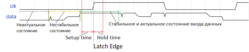
Figure: 2.Setup Time and Hold time as a guard interval around the capture edge at the clock input of the register
The Setup time and Hold time values are strictly defined by the FPGA manufacturer. They depend on the crystal production technology and are considered constants for analysis, the same for each register in the crystal. In any case, these values do not depend on the user in any way; their accounting is a task only for the time analysis utility. It is not important for us to know what they are equal to, it is important for us only to know that they exist and are not equal to zero.
The essence of the time analysis is to calculate the slacks in time for each pair of registers in the project, between which there is data transfer, that the data has to be stable during the guard interval. There are many such r2r pairs in the project, thousands, or even millions, but each of them must be analyzed in order to make sure that the project works.
There are also two slacks, respectively - Setup Slack and Hold Slack (Fig. 3).
Setup Slack characterizes the time margin that the data has from the moment of stabilization to the beginning of the Setup time interval.
Hold Slack characterizes the time margin that data has from the end of the Hold time interval to the loss of stability by the data.
Slacks must be positive. If the slack is negative, then the condition of stability of the input data is not met and the data will beat. The more slack - the better, but you need to understand that on each register-destination, its preset and hold slacks have one common time for two. This means that an increase in one slack always leads to a decrease in the other. Therefore, the best option is when both slacks are positive and approximately equal to each other, i.e. the balance of slacks is respected.
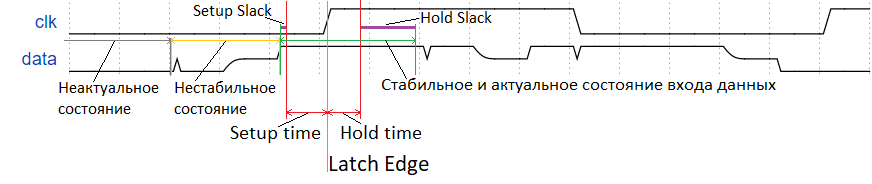
Figure: 3. Positive slacks, the condition for successful data reception is met, but there is no balance between the slacks
Slack calculation
Now let's move on to how these slacks are calculated. Let's start with Setup Slack.
Consider the data transfer scheme in Fig. 4.

Fig. 4. Data transfer scheme
Here we introduce such concepts as trigger front, capture front, data arrival time, data waiting time and clock arrival time.
The Launch Edge is the front of the clock that came to the input of the source register and started the data transfer process.
The Latch Edge is the clock front that arrives at the receiving register and forces it to grab data on input.
The moment of arrival of data ( Data Arrival Time ) is defined as the actual arrival of data at the receiving register.
The Data Required Time is defined as the time it takes for the data to reach the destination before the preset time on the destination register.
The time of arrival of a clock ( Clock Arrival Time ) is defined as the time of passage of the edge of the capture from the clock input of the entire circuit to the clock input of the receiver. Moreover, the capture front means the next front after the launch front. The launch front sends data from the source to the recipient, and after one clock period, the capture front catches this data on the recipient's side.
The clock input of the entire circuit is understood as a single point from where the clock diverges to all the registers operating on it. This is usually the output of the global clock buffer or the output of the PLL. In the most primitive case, this is the FPGA leg, to which the clock generator is connected.
The terms involved in the temporal analysis may not have a point value, but a certain range of possible values, depending on the design trace and the crystal temperature. Therefore, the worst slack is analyzed. The exchange of data is considered successful if, even in the worst conditions for a slack, it remains positive.
How does the moment of data arrival relate to the trigger edge?
We consider the arrival of data as passing through a chain with a register of some event initiated by a trigger edge.
The trigger front appears at the clock input of the system, then it reaches the input of the source register for some time, then for some time this register is triggered and sends new data to the output, then this data passes through the combinational logic circuits to the receiving register. The worst, slowest variant of data passage is considered, therefore the terms come with the "max" prefix.
In this formula, the term for the trigger edge carries the meaning of a reference point relative to which events develop, and not some value measured in nanoseconds.
TermIs the maximum time it takes for the trigger edge to go from the clock input of the entire circuit to the clock input of the source. As a rule, the analyzer simply takes the time range from “exactly not less than” to “exactly not more than” and substitutes the upper bound “definitely not more than” into this formula. This value is independent of the user. The compiler decides for itself where to place the register on the crystal and takes into account the time it takes for the clock to travel to it. The network of connections through which the clock signal diverges from the global clock buffer to registers is designed so that the clock signal reaches any register in almost the same amount of time. Therefore, in fact, the difference between and extremely small, but still taken into account.
Term- this is the clock-to-output time , which the register spends on seeing the edge at the clock input change the data at its output. The analyzer considers this value to be equal for all registers on the chip. This value is independent of the user.
The last termIs the maximum time for an event (data) to pass through the combination logic between registers, which is defined by the user. This value is highly dependent on the user. It expresses the amount of combinational logic between registers. In turn, long chains of combinational logic are often the result of inaccurate coding by the user.
The moment the shred arrives at the recipient is easier to calculate:
This is the earliest moment at which the capture edge will reach the clock input of the receive register.
Term- this is the minimum time for which the capture front will reach the recipient's clock input, that is, by analogy with the previous formula, this time is “definitely not less than”. The dash in this case means that we are talking about the clock input of the receiver, not the source.
The waiting time for data is defined as the time it takes for the data to reach the receiver before the preset time on the receiver register:
Term - this is already known to us Setup time, which is considered the same for each register on the crystal. This time is independent of the user.
TermIs Clock Setup Uncertainty , preset time uncertainty. Like any other uncertainty in the temporal analysis of a CSU is not a physical process, but a way to reflect the influence of jitter in the analysis, or simply a way to introduce a guard time into the analysis just in case. In simple words, this is a margin of time to take into account difficult processes.
Now that these terms are defined, we can define a preset slack as the smallest difference between the time that is allowed to travel to the destination and the time it actually takes.
Now let's expand these terms and rearrange them a little:
New terms have appeared here.
It is clear about the period, this is the period of the clock frequency, i.e. time between Launch Edge and Latch Edge.
Term- this is the clock skew - the minimum value of the spread of the arrival time of one clock edge from the clock input of the system to different synchronous registers. The minimum clock spread is defined as the difference between the smallest clock delay to the recipient and the largest clock delay to the source.... The analyzer makes no difference in estimating this time for different registers on the chip.
This is how we calculated the preset slack. A positive margin is good, a negative margin is bad. Slack literally translates to sagging. So if there is a slack, then the inter-register transfer is not configured "vnatyag", the conditional "thread" sags freely. Slack is negative - it means that the transmission thread was pulled over and broken.
Figure 5 shows how the slack formula can be represented graphically:
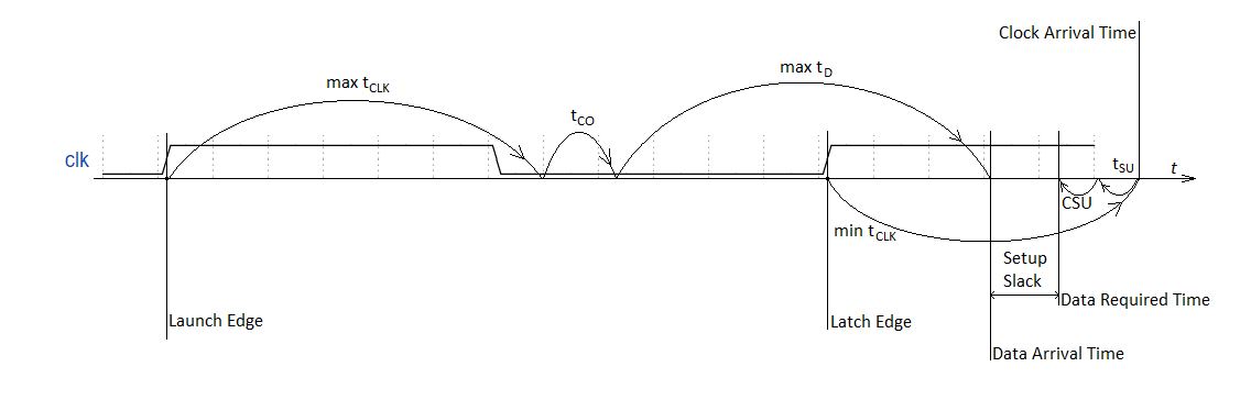
Fig. 5. Graphical Representation of the Setup Slack Expression
This shows the relationship in the background of the clock signal, and this is the clock signal at the clock input of the system, not at the input of any of the registers.
Now let's calculate the retention slack in a similar way .
It can also be represented by an expression in which the terms have changed signs:
These terms are now considered from the other side.
Now the fastest variant of data passage is considered here and where "max" was "min".
The moment of arrival of the clok front is also viewed in a different vein, as the latest possible:
It is important to note that in the case of Hold Slack, the Launch Edge and Latch Edge fronts are now the same front, rather than two different fronts separated by the clock period. In this situation, the receiving register needs to have time to hold the data at the input during the hold time from the arrival of the clock front. But the data is changed at its input by the same front, which came somewhere else to the source register. Therefore, in the analysis of the retention slack, the difference isequal to zero, not the period.
The required time in this case is defined as the time during which the data should not change at the input of the recipient's data, so as not to catch the hold time:
Term - this is already known to us Hold time, hold time. It is considered the same for every register on the chip and does not depend on the user.
TermIs Clock Hold Uncertainty , the uncertainty of the holding time. It carries in general the same meaning as CSU, and as a rule it is taken equal to it.
If, as in the case of the preset slack, you expand the terms and swap them, then the retention slack expression can be transformed into the following form:
Another look at this formula
Above, a method for calculating slacks was presented, which is characteristic of the human understanding of the processes taking place. Here "the front is coming ...", "data is coming ...". If you are interested, as a supplement, I will tell you how the analyzer of time constraints imagines these calculations.
The analyzer groups the terms differently, based on its machine reasons. But in the end it comes to the same result.
It uses the terms Clock Setup Relationship ( SR ) and Clock Hold Relationship ( HR ) - which can be translated as the ratio of the time between the trigger edges for preset and hold, respectively.
Figure 6 shows how these fronts are related:

Fig. 6. Fronts used in slack calculations.
You can immediately convert the resulting expressions into a more understandable form:
The longest inter-register time (Largest r2r Required) is the maximum time available for data to reach the destination before the start of the preset interval:
The longest inter-register delay (longest r2r Delay) is the time it takes to transfer data from the source register to the destination register along the longest path:
We can now define the preset slack as the difference between the time available to reach the destination register and the actual time to get there:
Expanding the terms of this formula will give us the familiar representation of the preset slack:
Now about the retention slack. The smallest r2r Requirement is the time it takes to hold data at the input of the destination register:
Shortest inter-register delay:
Now we define the slack of the preset as the difference between the fastest time for data to leave the receiver's input and the time it takes to keep it there:
When expanding the terms, the expression also takes on the already familiar form:
What conclusions can be drawn from boring formulas?
We have seen how slacks are calculated. How to use this knowledge?
Let's look at the slack expressions again:
If some slacks of the project became negative, then we can change them by changing their terms. That is, we see how we can fix bad slacks.
We see terms that do not depend on the user, but depend only on the crystal technology. it... There is no way to interfere.
We see the terms CSU and CHU, which the analyzer usually takes equal to the CU parameter - Clock Uncertainty, the instability of the clock frequency. Generally speaking, this parameter is small, tens of picoseconds. It is specified by the user in the restrictions file. And the user, in turn, takes it from the specification for the clock generator. It is considered that a clock buffer or internal FPGA PLL, which receives an external clock from the oscillator and converts it to an internal clock at the system clock input, keeps the CU value the same as that received from the oscillator. If CU is not specified, the analyzer will set it to some default value, for example, Quartus sets it to 20 ps. In the general case, this term tells us that it is better to use highly stable oscillators with a small amount of instability for clocking. Good oscillators are in the order of 20-60 ps.
The period term shows that the obvious way to combat data transmission misdirection is to reduce the clock frequency. It is reasonable, but not always acceptable, since the terms of reference usually requires some system performance, below which you cannot go. And performance directly depends on the clock speed. We can also see the difference between the preset and hold slacks - the hold slack is independent of frequency.
And finally, the termessentially characterizes the efficiency of the written code. Hence, the main way to solve slack problems is to rewrite it properly. Big timeappears in too complex hardware designs that require too much combinational logic. If you have such complex constructions in your project, then the classic way to solve the problem is to split one complex r2r transfer into several simple ones by inserting another 1-2 registers into the sequence of operations. In this case, the delay in cycles for the operation will increase, but the operation speed will increase. For example, adding several vectors in one clock cycle is not a good idea. It is better to add several vectors one by one, with intermediate sums. Some complex constructions can sometimes be impossible to break into a pipeline of several simple ones - then such logic must be rewritten in some way fundamentally different.
Conclusion
The point of this article is to learn about the existence of the concept of a slack and what this slack physically depends on. Knowing this, you can independently study the reports of the analyzer of time constraints, draw conclusions and debug the performance of your project. These are formulas by which you will hardly ever have to do a real calculation. You don't even need to remember them by heart. It is only important to grasp the logic of what is happening in the interregister transfer and to understand what factors determine the speed of the project.