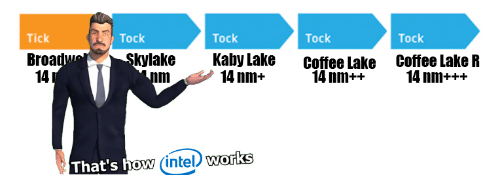
Where is Intel in general? Just barely crawled 10 nm?
We decided to find out what these nanometers measure? And is it so important to measure them or is it just marketing? And is Intel really so godlessly outdated?
Before moving on to the processors in our smartphones and computers, a little basics, how does a processor work?
Meet this transistor! A key element of all processors. In fact, a transistor is a switch. The current flows through it - this is 1, the current does not flow - this is 0. This allows counting in the binary system - the basis of all processors!
Previously, transistors were vacuum bulbs. Conditional - on or off: one or zero.
There were a lot of such bulbs for everything to work somehow. For example, the 1946 ENIAC computer that helped create the hydrogen bomb had 17.5 thousand vacuum tubes and weighed 27 tons, occupying 167 square meters. At the same time, he ate 150 kW of electricity.
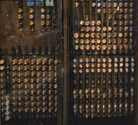
And here is one of the key points worth paying attention to. Once again, the power consumption of these 17.5 thousand bulbs was 150 kW.


But in the early 1960s, there was a revolution - the invention and beginning of production of field-effect transistors. They have silicon as their initial semiconductor - hence the well-known silicon, ahem, that is, Silicon Valley!
And then it started! The size of transistors has decreased so much that they consume significantly less electricity and take up less space. And the number of transistors in computing began to increase at a tremendous rate! And with it the power of computing systems!

The first industrial processor Intel 4004, which was released in 1971, had 2,250 transistors.
And now, for example, in the A13 Bionic of these transistors 8.5 billion - that's more than people on the planet! Then bye…
But how much have modern transistors actually decreased, how small are they? Simple comparison, easy to understand - for example, with a human hair!
Almost 1.5 million modern transistors made using a 7-nanometer process technology can be placed on its cut!
That is, you can place 4 times more transistors on the thickness of a human hair than in the Intel 4004 processor!
Why should it be reduced? Everything is more or less obvious here!
First, the smaller the transistor, the less power it consumes. You already understood this with the example of tube ones.
And secondly, there are more of them on the die, which means that productivity increases. Double benefit!
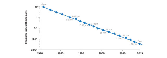
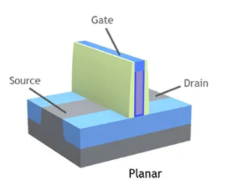
And here we move on to the concept of a technical process or Technology Node - what is it?
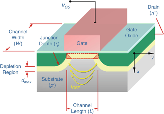
If to simplify as much as possible, then the value of the technical process has historically been the minimum length of the transistor channel - as you can see in the picture, it should not be confused with the size of the entire transistor.
That is, the smaller the size of the technical process, the better - this is what the companies are trying to convey to us, but is everything so simple?
And here something else is important: transistors are different and they differ not only in size, but also in their structure.
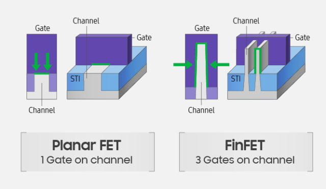
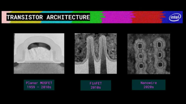
Classic, planar or flat, transistors have ceased to be used relatively recently - in 2012. They gave way to three-dimensional transistors, where they extended the channel into the third dimension, reducing its thickness and thereby reducing the transistor itself. This structure is called FinFET and they are used now.

This technology helped a lot to reduce the size of transistors and, most importantly, it greatly increased the number of transistors per unit area, which is one of the key performance indicators!
But does the concept of technical process mean the same today as it did a few years ago?
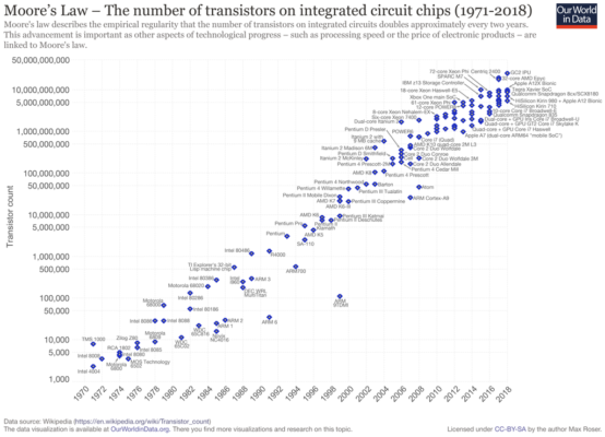
A very important trend was observed throughout the industry - each subsequent technical process was 30% less than the previous one, which helped to double the number of transistors while maintaining the same power consumption - for example, 130 * 0.7 = 90 nm, 90 * 0.7 = 65 nm, then up to 45 nm, 32 nm, and so on.
And this is still in line with Moore's Law:
The number of transistors on an integrated circuit chip doubles every 24 months.
What's behind this numbers game?
We have already found out that the technical process is the size of the transistor gate, that is, the length of the channel that passes or does not pass current through itself, and this size is key!
But it turns out this is true only if we are talking about the old 32 nm - everything is accurate there, even if you measure it with a ruler! And this parameter was documented!
But this was until 2009, when the concept of a technical process and its designation was excluded from the so-called “International plan for the development of semiconductor technology”!
In simple terms - the numbers indicated in those processes today are just a marketing label!
Manufacturers went wild and started calling everything 10, 7 and generally 5 nanometers, and someone is already talking about 3 nanometers! You can put all this in quotes, as a simple designation of a generation of processors!

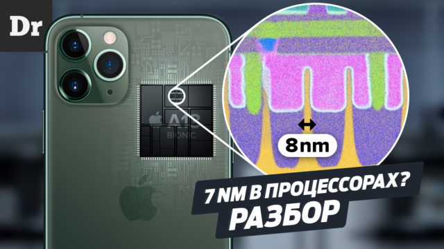
Here's an example of the structure of the Apple A12 processor, produced at the TSMC plant using a 7-nanometer process technology. Pay attention to the scale scale in the lower left corner.

If we compare the scale and calculate, it turns out that the channel width is 8 nanometers, despite the fact that the process is officially called 7-nanometer.
Now let's compare Intel's 10nm process and TSMC's 7nm process.
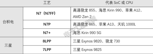
By the way, know that today TSMC is a company that manufactures processors for AMD, and also makes Apple A13 and Snapdragon 865 - so consider that we are comparing all their chips at once.
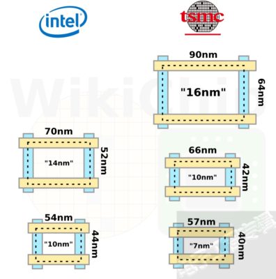
Pay attention to the dimension. You can immediately see that the same 10nm from Intel is almost the same as 7nm from TSMC! So Intel is not that far behind AMD and other manufacturers - have they just lost the marketing battle? Here, too, everything is not so simple!

Suddenly Intel even outperforms TSMC in some ways.
Look at 1 square millimeter of a 10nm Intel die, about 5 percent more transistors fit than a 7nm one from Apple, Qualcomm, or AMD.
But at the same time, the increased density has its disadvantages - increased heating!
It means that Intel crystals are more powerful, but due to their density they heat up more. Thus, we get the same notorious throttling.
And processors manufactured by TSMC - Apple Qualcomm and AMD benefit precisely due to the more spacious arrangement of transistors of about the same size.
How they do it is more a matter of internal architecture, and not a number that is in the name of those processes.
Do not think that I have forgotten about the N7FF + architecture - yes, it is even denser than Intel, but if we talk about AMD Zen 2, Appl A13, Snapdragon 865 chips - all are made on the basis of TSMC 7FF and it loses in Intel density.
The only processor already produced with the new N7FF + technology using extreme UV lithography is the Kirin 990 5G. Here, of course, the density of transistors increases greatly - by as much as 15 percent!

In theory, manufacturers just follow a slightly different path, and if you look into the future, it becomes clear which one: here's a sign of how everything will be - next-generation chips.
We are interested in the line about the density of transistors per square millimeter!
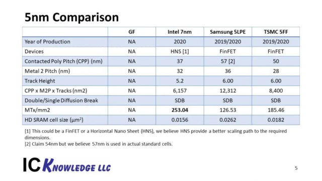
According to these data, Intel by more than 30 percent bypasses both Samsung and TSMC in the density of transistors - and this despite the fact that here we are already comparing 7 nm from one manufacturer and 5 from another.
Where does this increase come from? How is such an increase in density possible - the prots will simply explode or work only with a fancy cooling system?
Not certainly in that way. The fact is that Intel plans to switch to transistors of a completely different structure - called HNS - Horizontal Nano Sheets - this will allow us to make the leap!

But Samsung has similar plans - they go a little the other way towards the Gate-All-Around FET structure.
This is how it looks in reality - not so cute, but just think about how small they are!
As a result, we realized that behind the marketing names of 7 nm and 5 nm there is a battle of architectures, and in the future we will be able to find out whose path was the right one.
What can be said absolutely for sure - we are in for a huge leap among all chips, both mobile and desktop, within the next few years.
On this note, I don't want to end the topic of processors, because we have studied a lot of information and documents, including sorted it out during the production process. For example, have you heard of this process Extreme Ultraviolet Lithography? If on the fingers, this is some kind of fantasy - a drop of tin turns into plasma after a laser hit: this is how modern processors are created. But the installations themselves can be created by only one company in the world, and all the giants depend on it.