
Previous articles in the series
Perhaps, today I will even break the tradition and will debug the project not on the Redd complex, but on a regular layout. Firstly, I am aware that the vast majority of readers do not have access to such a complex, but they have access to Ali Express. Well, and secondly, I'm just too lazy to fence a garden with a pair of USB-device and host connected, and also to deal with the emerging interference.
Back in 2017, I was looking for ready-made solutions on the network and found such a wonderful thing , or rather, its ancestor. Now they have everything on a specialized board, but then everywhere there were photos of a simple breadboard from Xilinx, to which a board from WaveShare was connected (you can learn about it here ). Let's take a look at the photo of this board.

It has two USB connectors at once. Moreover, the diagram shows that they are parallelized. You can plug your USB devices into a type A socket, and you can connect a cable to the mini USB connector, which we will plug into the host. And the description of the OpenVizsla project says that this way works. The only pity is that the project itself is rather difficult to read. You can take it on github, but I will give a link not to the account that is indicated on the page, everyone will find it anyway, but it has been redone for MiGen, but the version that I found in 2017: http: // github. com / ultraembedded / cores, it's on a clean Verilog, and there is the usb_sniffer branch. There, everything goes not directly through ULPI, but through the ULPI to UTMI converter (both of these obscene words are such physical level microcircuits that match the high-speed USB 2.0 channel with buses understandable to processors and FPGAs), and only then work with this UTMI. How everything works there, I have not figured out. Therefore, I preferred to make my development from scratch, since we will soon see that everything is scary there rather than difficult.
What hardware can you work on
The answer to the question from the title is simple: on anyone with an FPGA and external memory. Of course, in this series we will only consider Altera FPGAs (Intel). However, keep in mind that the data from the ULPI microcircuit (it is on that handkerchief) runs at 60 MHz. Long wires are not acceptable here. It is also important to connect the CLK line to the FPGA input from the GCK group, otherwise everything will work and then fail. Better not to risk it. I do not advise you to programmatically forward it. I tried. It all ended with a wire to the leg from the GCK group.
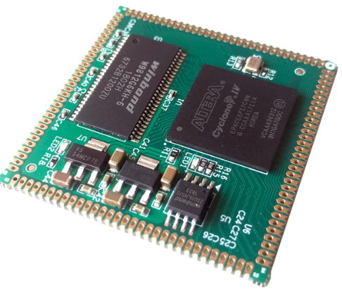
For today's experiments, at my request, a friend soldered to me such a system:

Micromodule with FPGA and SDRAM (look for it on ALI express by the phrase FPGA AC608) and the same ULPI board from WaveShare. This is how the module looks in the photos from one of the sellers. I'm just too lazy to unscrew it from the case:
By the way, the ventilation holes, as in the photo of my case, are very interesting. On the model, draw a solid layer, and in the slicer set the fill to, say, 40% and say that you need to make zero solid layers below and above. As a result, the 3D printer draws this ventilation itself. Very comfortably.
In general, the approach to finding hardware is clear. Now we start designing the analyzer. Rather, we have already made the analyzer itself in the last two articles ( here we worked with hardware , and here - with access to it ), now we will simply design a problem-oriented head that catches data coming from the ULPI microcircuit.
What the head should be able to do
In the case of the logic analyzer, everything was easy and simple. There is data. We connected to them and started packing, and sending them to the AVALON_ST bus. Everything is more complicated here. The ULPI specification can be found here . Ninety-three sheets of boring text. Personally, this drives me into despondency. The description for the USB3300 chip, which is installed in the WaveShare board, looks a little simpler. You can get it here . Although I still accumulated courage since that very December 2017, sometimes reading the document and immediately closing it, as I felt the approach of depression.
From the description it is clear that ULPI has a set of registers that must be filled in before starting work. This is primarily due to pull-up and terminating resistors. Here is a picture to explain the point:

Depending on the role (host or device), as well as the selected speed, different resistors must be included. But we are neither a host nor a device! We must disconnect all resistors so as not to interfere with the main devices on the bus! This is done by writing to registers.
Well, and speed. It is necessary to choose a working speed. To do this, you also need to write to the registers.
When we have everything configured, you can start fetching data. But in the name of ULPI, the letters "LP" mean "Low Pins". And this very reduction in the number of legs led to such a furious protocol that just hold on! Let's take a closer look at the protocol.
ULPI protocol
The ULPI protocol is somewhat unusual for the common man. But if you sit with a document and meditate, then some more or less understandable features begin to appear. It is becoming clear that the developers have made every effort to really reduce the number of contacts used.
I will not retype the complete documentation here. Let's limit ourselves to the most important things. The most important of these is the direction of the signals. It is impossible to remember it, it is better to look at the picture every time:

ULPI LINK is our FPGA.
Timing diagram of data reception
At rest, we must issue a constant 0x00 to the data bus, which corresponds to the IDLE command. If data comes from the USB bus, the exchange protocol will look like this:
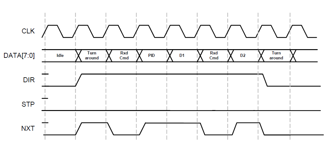
The cycle will begin with the fact that the DIR signal will fly up to one. First, it will be there one clock cycle so that the system has time to switch the direction of the data bus. Further - miracles of economy begin. See the name of the NXT signal? It means NEXT when transmitted from us. And here it is a completely different signal. When DIR is one, I would call NXT C / D. Low level - we have a team. High - data.
That is, we must fix 9 bits (the DATA bus and the NXT signal) either always at a high DIR (then filtering the first clock by software), or starting from the second clock after DIR takes off. If the DIR line falls to zero, we switch the data bus to write and again start broadcasting the IDLE command.
With data reception - it's clear. Now let's analyze the work with registers.
Timing diagram of writing to the ULPI register
To write to the register, the following temporary house is used (I deliberately switched to jargon, because I feel that I am tending towards GOST 2.105, and this is boring, so I will
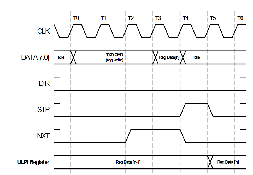
move away from it): First of all, we must wait for the state DIR = 0. At clock T0, we must set the TXD CMD constant on the data bus. What does it mean? You can't figure it out right away, but if you dig a little through the documents, it turns out that the desired value can be found here:

That is, the high data bits should be set to the value "10" (for the entire byte, the mask is 0x80), and the lower ones - the register number.
Next, you should wait for the NXT signal to take off. With this signal, the microcircuit confirms that it heard us. In the picture above, we waited for it at clock T2 and set the data on the next clock (T3). On clock T4, the ULPI will receive the data and remove the NXT. And we will mark the end of the unit exchange cycle in STP. On also T5, the data will be latched into the internal register. The process has ended. Here's a payback for a small number of conclusions. But we will need to write the data only at startup, so, of course, we will have to suffer with development, but all this will not particularly affect the work.
Timing diagram of reading from ULPI register
Honestly, for practical tasks, reading registers is not so important, but let's look at it too. Reading will be useful at least to make sure that we have implemented the record correctly.
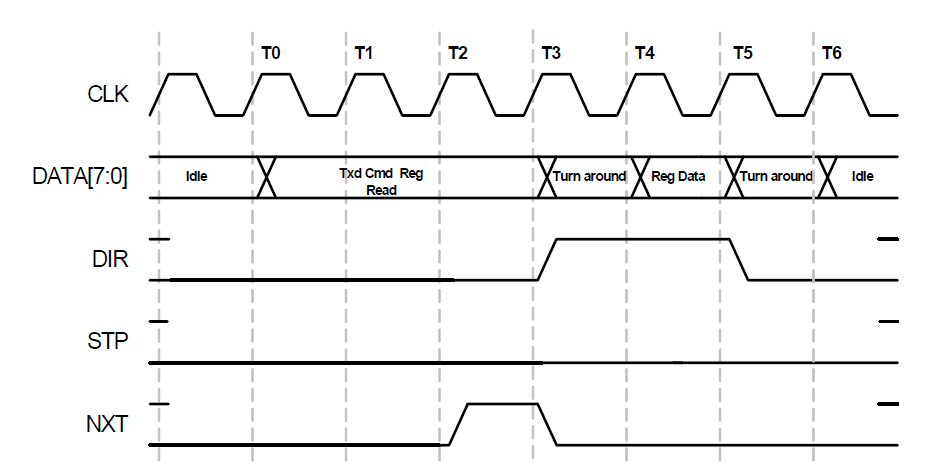
We see that before us is an explosive mixture from the previous two temporary houses. We set the address as we did for writing to the register, and we take the data according to the rules for reading data.
Well? Let's start designing an automaton that will shape all this for us?
Structural diagram of the head
As you can see from the description above, the head must be connected to two buses at once: AVALON_MM to access registers and AVALON_ST to send data to be stored in RAM. The main thing in the head is the brain. And so it should be a state machine that will generate the time diagrams that we considered earlier.

Let's start its development with the function of receiving data. It should be borne in mind here that we cannot influence the flow from the ULPI bus in any way. Data from there, if it started to go, it will go. They don't care whether the AVALON_ST bus is ready or not. Therefore, we will simply ignore the unavailability of the bus. In a real analyzer, it will be possible to add an alarm indication in case of data output without readiness. Everything should be simple within the framework of the article, so let's just remember this for the future. And to ensure the availability of the bus, as in a logic analyzer, we will have an external FIFO block. In total, the transition graph of the automaton for receiving the data stream is as follows:
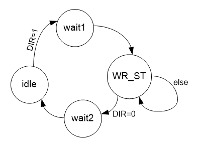
DIR took off - began to receive. We hung one clock in wait1, then we accept it while DIR is equal to one. Fell to zero - after a clock (though not the fact that it is needed, but for now we will set the state wait2) returned to idle.
So far, everything is simple. Do not forget that not only the D0_D7 lines, but also the NXT line should go to the AVALON_ST bus, since it determines what is being transmitted now: a command or data.
A register write cycle can have an unpredictable execution time. From the point of view of the AVALON_MM bus, this is not very good. Therefore, we will make it a little trickier. Let's create a buffer register. The data will get into it, after which the AVALON_MM bus will be immediately released. From the point of view of the automaton being developed, the have_reg input signal appears (data in the register has been received, which should be sent) and the reg_served output signal (meaning that the register issuance process is completed). Add the logic of writing to the register on the transition graph of the automaton.
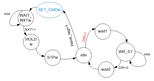
I have highlighted the DIR = 1 condition in red to make it clear that it has the highest priority. Then it is possible to exclude the expectation of the zero value of the DIR signal in the new branch of the automaton. Logging into a branch with a different value will simply not be possible. The SET_CMDw state is blue as it is most likely to be purely virtual. These are just actions to be performed! Nobody bothers to set the corresponding constant on the data bus and just during the transition! In the STPw state, among other things, the reg_served signal can also be cocked for one clock cycle to clear the BSY signal for the AVALON_MM bus, allowing a new write cycle.
Well, it remains to add a branch for reading the ULPI register. Here, the opposite is true. The bus service machine sends us a request and waits for our response. When the data is received, he can process it. And it will work with bus suspension or polling, these are already the problems of that machine. Today I decided to work on a survey. Requesting data - BSY appeared. How BSY disappeared - you can receive read data. In total, the graph takes the form:
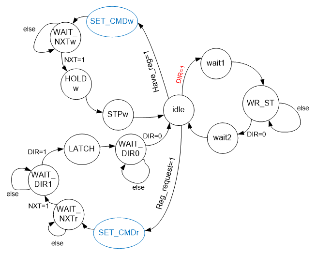
Perhaps, in the course of development, there will be some adjustments, but for now, we will adhere to this graph. After all, this is not a report, but an instruction on the development methodology. And the technique is such that first you need to draw a transition graph, and then - do the logic, according to this figure, adjusted for pop-up details.
Features of the automaton implementation from the AVALON_MM side
When working with the AVALON_MM bus, you can go in two ways. The first is to create bus access delays. We explored this mechanism in one of the previous articles , and I warned that it is fraught with problems. The second way is classic. Enter the status register. At the beginning of the transaction, set the BSY signal, at its completion - reset. And assign responsibility for everything to the bus master logic (Nios II processor or JTAG bridge). Each of the options has its own advantages and disadvantages. Since we have already done variants with bus delays, let's do everything today, for a change, through the status register.
We design the main machine
The first thing I would like to draw your attention to are my favorite RS triggers. We have two machines. The first serves the AVALON_MM bus, the second - the ULPI interface. We found out that the connection between them goes through a couple of flags. Only one process can write to each flag. Each automaton is implemented by its own process. How to be For some time now, I just started adding an RS trigger. We have two bits, so they must be generated by two RS flip-flops. Here they are:
//
always_ff @(posedge ulpi_clk)
begin
      //
      if  (reg_served)
           write_busy <= 0;
      else if (have_reg)
           write_busy <= 1;

      //
      if  (read_finished)
           read_busy <= 0;
      else if (reg_request)
           read_busy <= 1;
end
One process cocks reg_served, the second one cocks have_reg. And the RS-flip-flop in its own process generates the write_busy signal on their basis. Similarly, read_busy is formed from read_finished and reg_request. You can do it differently, but at this stage of the creative path, I like this method.
This is how BSY flags are set. Yellow is for the writing process, blue for the reading process. The Verilogov process has one very interesting feature. In it, you can assign values not once, but several times. Therefore, if I want a signal to take off for one clock cycle, I nullify it at the beginning of the process (we see that both signals are nullified there), and set it to one by a condition that is executed during one clock cycle. Entering the condition will override the default. In all other cases, it will work. Thus, writing to the data port initiates the takeoff of the have_reg signal for one clock cycle, and writing bit 0 to the control port initiates the takeoff of the reg_request signal.

The same text.
//  AVALON_MM
always_ff @(posedge ulpi_clk)
begin
   //    ,
   //
   have_reg    <= 0;
   reg_request <= 0;

   if (write == 1)
   begin
      case (address)
          0 : addr_to_ulpi <= writedata [5:0];
          //
          1 : begin
                data_to_ulpi <= writedata [7:0];
                have_reg <= 1;
              end
          2 : begin
                //
                reg_request <= writedata[0];
		force_reset = writedata [31];
              end
         3: begin end
      endcase
   end
end
As we saw above, one clock cycle is enough for the corresponding RS flip-flop to set to one. And from this moment, the set BSY signal starts to be read from the status register:

The same text.
//  AVALON_MM
always_comb
begin
   case (address)
      //   (  )
      0 : readdata <= {26'b0, addr_to_ulpi};

      //
      1 : readdata <= {23'b0, data_from_ulpi};

      // 2 -  ,   -

      //
      3 : readdata <= {30'b0, (reg_request | read_busy), (have_reg | write_busy)};
      default: readdata <= 0;
   endcase
end
Actually, so naturally we got acquainted with the processes serving work with the AVALON_MM bus.
Let me also remind you about the principles of working with the ulpi_data bus. This bus is bi-directional. Therefore, you should use a standard technique for working with it. This is how the corresponding port is declared:
inout [7:0] ulpi_data,
We can read from this bus, but we cannot write directly. Instead, we create a copy for the record.
logic [7:0] ulpi_d = 0;
And we connect this copy to the main bus through the following multiplexer:
//      inout-
assign ulpi_data = (ulpi_dir == 0) ? ulpi_d : 8'hzz;
I tried to comment on the logic of the main machine as much as possible inside the Verilog code. As I expected during the development of the transition graph, in real implementation, the logic has changed somewhat. Some of the states were thrown out. Nevertheless, comparing the graph and the source text, I hope you understand everything that is done there. Therefore, I will not talk about this machine. It is better to give for reference the full text of the module, relevant at the time before the modification based on the results of practical experiments.
Full text of the module.
module ULPIhead
(
   input               reset,
   output              clk66,

   // AVALON_MM
   input        [1:0]  address,
   input               write,
   input        [31:0] writedata,
   input               read,
   output logic [31:0] readdata = 0,

   // AVALON_ST
   input  logic        source_ready,
   output logic        source_valid = 0,
   output logic [15:0] source_data = 0,

   // ULPI
   inout        [7:0]  ulpi_data,
   output logic        ulpi_stp = 0,
   input               ulpi_nxt,
   input               ulpi_dir,
   input               ulpi_clk,
   output              ulpi_rst
);

logic      have_reg = 0;
logic      reg_served = 0;
logic      reg_request = 0;
logic      read_finished = 0;
logic [5:0] addr_to_ulpi;
logic [7:0] data_to_ulpi;
logic [7:0] data_from_ulpi;

logic      write_busy = 0;
logic      read_busy = 0;

logic [7:0] ulpi_d = 0;

logic force_reset = 0;

//
always_ff @(posedge ulpi_clk)
begin
      //
      if  (reg_served)
           write_busy <= 0;
      else if (have_reg)
           write_busy <= 1;

      //
      if  (read_finished)
           read_busy <= 0;
      else if (reg_request)
           read_busy <= 1;
end

//  AVALON_MM
always_comb
begin
   case (address)
      //   (  )
      0 : readdata <= {26'b0, addr_to_ulpi};

      //
      1 : readdata <= {23'b0, data_from_ulpi};

      // 2 -  ,   -

      //
      3 : readdata <= {30'b0, (reg_request | read_busy), (have_reg | write_busy)};
      default: readdata <= 0;
   endcase
end

//  AVALON_MM
always_ff @(posedge ulpi_clk)
begin
   //    ,
   //
   have_reg    <= 0;
   reg_request <= 0;

   if (write == 1)
   begin
      case (address)
          0 : addr_to_ulpi <= writedata [5:0];
          //
          1 : begin
                data_to_ulpi <= writedata [7:0];
                have_reg <= 1;
              end
          2 : begin
                //
                reg_request <= writedata[0];
		force_reset = writedata [31];
              end
         3: begin end
      endcase
   end
end

//
enum {idle,
wait1,wr_st,
wait_nxt_w,hold_w,
wait_nxt_r,wait_dir1,latch,wait_dir0

} state = idle;
always_ff @ (posedge ulpi_clk)
begin
   if (reset)
   begin
       state <= idle;
   end else
   begin
      //
      source_valid <= 0;
      reg_served  <= 0;
      ulpi_stp <= 0;
      read_finished <= 0;
      case (state)
      idle: begin
           if (ulpi_dir)
               state <= wait1;
           else if (have_reg)
                begin
                  //      ,
                  //    ,
                  //
                  ulpi_d [7:6] <= 2'b10;
                  ulpi_d [5:0] <= addr_to_ulpi;
                  state <= wait_nxt_w;
                end
           else if (reg_request)
                begin
                  //  -
                  ulpi_d [7:6] <= 2'b11;
                  ulpi_d [5:0] <= addr_to_ulpi;
                  state <= wait_nxt_r;
                end
         end
      //      TURN_AROUND
      wait1 : begin
            state <= wr_st;
            //    ,
            source_valid <= 1;
            source_data <= {7'h0,!ulpi_nxt,ulpi_data};
         end
      //     DIR -    AVALON_ST
      wr_st : begin
            if (ulpi_dir)
            begin
              //   ,
               source_valid <= 1;
               source_data <= {7'h0,!ulpi_nxt,ulpi_data};
            end else
               //      wait2,
               //   ,   - .
               state <= idle;
         end
      wait_nxt_w : begin
           if (ulpi_nxt)
           begin
              ulpi_d <= data_to_ulpi;
              state <= hold_w;
           end
         end
      hold_w: begin
           //   ,  ULPI
           //     .   NXT
           //  ...
           if (ulpi_nxt) begin
              // ,  AVALON_MM
              reg_served  <= 1;
              ulpi_d <= 0;    //   idle
              ulpi_stp <= 1;  //     STP
              state <= idle;  //   -    idle
           end
         end
       //   STPw   ...
       // ...
      //    . ,   NXT
      //    ,
      wait_nxt_r : begin
           if (ulpi_nxt)
           begin
              ulpi_d <= 0;    //
              state <= wait_dir1;
           end
         end
      // ,
      wait_dir1: begin
          if (ulpi_dir)
             state <= latch;
        end
      //
      //   -
      latch: begin
          data_from_ulpi <= ulpi_data;
          state <= wait_dir0;
        end
      // ,
      wait_dir0: begin
          if (!ulpi_dir)
          begin
             state <= idle;
             read_finished <= 1;
          end
        end

      default:	begin
         state <= idle;
         end
      endcase
    end
end
//      inout-
assign ulpi_data = (ulpi_dir == 0) ? ulpi_d : 8'hzz;

// reset   ,
assign ulpi_rst = reset | force_reset;

assign clk66 = ulpi_clk;

endmodule
Programmer's Guide
ULPI register address port (+0)
The address of the ULPI register of the bus, with which the work will go, should be placed in the port with offset +0
ULPI Register Data Port (+4)
When writing to this port: the process of writing to the ULPI register, the address of which was set in the port of the register address, starts automatically. It is forbidden to write to this port until the process of the previous write has finished.
On Read: This port will return the value obtained from the last read from the ULPI register.
ULPI control port (+8)
The read is always zero. The bit assignment for writing is as follows:
Bit 0 - When writing a single value, initiates the process of reading the ULPI register, the address of which is set in the address port of the ULPI register.
Bit 31 - When writing one, sends a RESET signal to the ULPI chip.
The rest of the bits are reserved.
Status port (+ 0x0C)
Read-only.
Bit 0 - WRITE_BUSY. If equal to one, the process of writing to the ULPI register is in progress.
Bit 1 - READ_BUSY. If equal to one, the process of reading from the ULPI register is in progress.
The rest of the bits are reserved.
Conclusion
We got acquainted with the method of physical organization of the USB analyzer head, designed a basic automaton for working with the ULPI microcircuit and implemented a draft SystemVerilog module for this head. In subsequent articles, we will look at the modeling process, simulate this module, and then conduct practical experiments with it, based on the results of which we will cleanly finalize the code. That is, until the end we have at least four more articles.