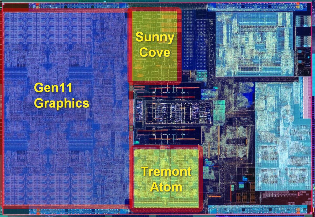
Intel Lakefield Processor Chip Diagram: One Core (Sunny Cove) and Four Atom (Tremont) Cores
Ten years ago, ARM introduced a heterogeneous architecture for big.LITTLE multi-core processorswith different cores: some were high performance and others were energy efficient. This hybrid system significantly reduced CPU power consumption while applications were running in the background (that is, almost always). The result was an increase in the operating time of the devices.
In 2019, the heterogeneous architecture was finally used by Intel for the first time in x86 processors. In 2020, two Lakefield processors with a 1 + 4 configuration (one Core and four Atom cores) will enter the market, writes AnandTech.
Lakefield Processors
| Intel Lakefield Processors | ||||||||
| Kernels |
|
1
|
nT
|
Gen11
IGP |
IGP
|
DRAM
LP4 |
TDP | |
| i5-L16G7 | 1+4 | 1400 | 3000 | 1800 | 64 EU | 500 | 4267 | 7 |
| i3-L13G4 | 1+4 | 800 | 2800 | 1300 | 48 EU | 500 | 4267 | 7 |
CPU
| Lakefield | |||||
| Intel
i7-L16G7 |
Intel
i3-1005G1 |
Intel
m3-8100Y |
Intel
N5030 |
Qualcomm
SD 7c |
|
| SoC | Lakefield | Ice
Lake-Y |
Amber
Lake-Y |
Goldmont+ | Kryo |
| 1+4 | 2+0 | 2+0 | 0+4 | 0+8 | |
| TDP | 7 | 9 | 5 | 6 | ~7 |
| CPU | 1 x SNC
4 x TNT |
2 x SNC | 2 x SKL | 4 x GMN+ | 8 x Kryo |
| GPU | Gen 11
64 EU 0,5 |
Gen 11
32 EU 0,9 |
Gen 9
24 EU 0.9 GHz |
Gen 9
18 EU 750 MHz |
Adreno
618 |
| LPDDR | 4267 | 3733 | LPD3-1866 | 2400 | 4267 |
| Wi-Fi | Wi-Fi 6 * | Wi-Fi 5 * | - | - | Wi-Fi 6 |
| Modem | - | - | - | - | Cat15 / 13 |
Benchmarks
The processors themselves have not yet appeared in the public domain, so it remains only to focus on benchmarks from Intel. The company gives only two comparisons: with Amber Lake-Y, that is, the 5W i7-8500Y, and the i5-L16G7 with itself in 1 + 4 and 0 + 4 modes (in fact, a comparison with the quad-core Atom design).
On the first point in comparison with Amber Lake-Y:
- + 12% SPEC2006 single thread performance (3.0 GHz for Lakefield vs. 4.2 GHz for Amber Lake-Y)
- + 70% 3DMark11 graphics performance versus HD615 (24 EU, Gen 9.5 @ 1.05 GHz, 2x4 GB LPDDR3-1866) vs. HD (64 EU, Gen11 @ 500 MHz, 2x4 GB LPDDR4X-4267)
- + 24% energy efficiency per watt on WebXPRT 3
- + 100% AI load on graphics, ResNet50 128 package on OpenVINO
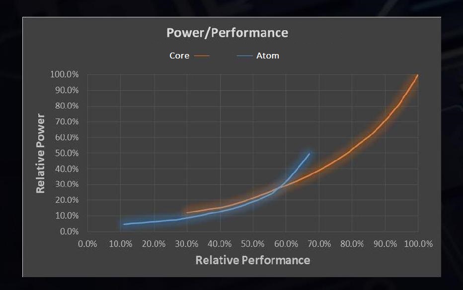
Mode 1 + 4 compared to 0 + 4 gives an increase of 33% in web performance and + 17% in energy efficiency. Basically, for most tasks, Lakefield will run like a quad-core Atom.
Factory tested for durability of Intel Lakefield processors. Photo: AnandTech
Why does a processor need a “big” core? It is needed to handle the highest priority interrupts when it is necessary to provide the minimum latency: pressing the screen, typing on the keyboard, and the like. This guarantees the responsiveness of the device even at the moments of maximum load of the other four cores.
How heterogeneous CPUs work
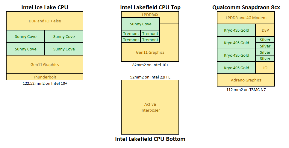
Lakefield combines one large Core and four small Atom cores on a single chip. In common reviews, these x86 processors may be called "five-core" and are usually written as 1 + 4.
Processor size 12 * 12 mm
Intel's goal is to combine the advantages of the energy-efficient Atom core with the more power-hungry, but more power-hungry Core core. The result is an intermediate processor between the “all Atom” 0 + 4 and “all Core” 4 + 0 designs.
The easiest way to compare Lakefield is to the older quad-core Atom processors, which added a large core. A cluster of four smaller Atom cores takes care of large concurrent workloads, while a large core reacts when the user loads an application or taps the screen, or scrolls through the browser.
The hybrid architecture is already used in ARM processors and even in Windows operating systems, like the Qualcomm Snapdragon processors in laptops like the Lenovo Yoga (4 + 4 design). Qualcomm has worked a lot with Microsoft to develop an appropriate scheduler that can manage workloads between different processor core designs.
Design visualization of different heterogeneous CPU architectures (no scale)
The main difference between Qualcomm and Intel is in software support: Qualcomm processors execute ARM instructions, while Intel processors execute x86 instructions. Most Windows programs are built for x86 instructions, which limits Qualcomm's performance in the traditional laptop market. Qualcomm's design actually allows for "x86 streaming," but the scope is limited and there is a performance penalty. However, work in this direction continues.
Foveros 3D layout
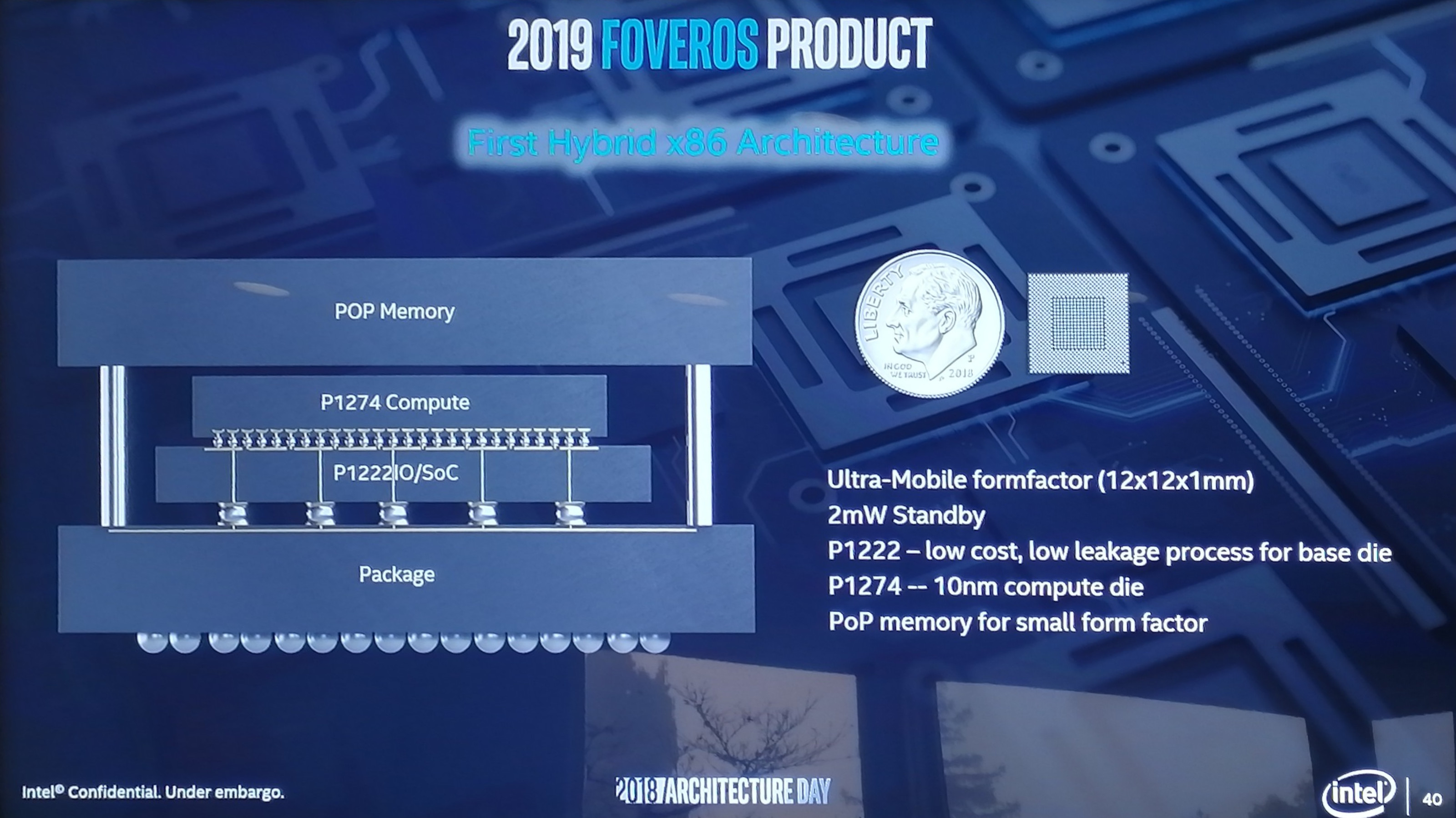
The entire microcircuit is placed in a 12 * 12 mm 2 case, so the real silicon is much smaller in size: the area of the lower microcircuit is 92 mm 2 , and the upper one is 82 mm 2.
The general design of a CPU with a three-dimensional layout of Foveros is shown in the diagram above. As you can see, the main computing microcircuit is located on top, and the base one is located below.
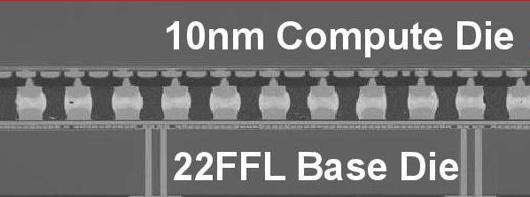
The upper 13-layer is manufactured using the 10 nm process technology, and the lower 10-layer one is manufactured using the 22 FFL process technology.
Computing microcircuit
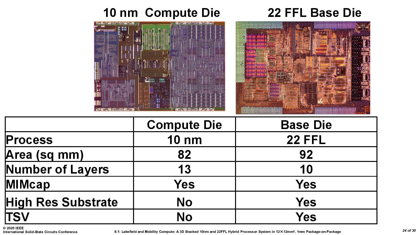
As indicated in the table, the microcircuits differ from each other and are manufactured using a different process technology.
Gen 11 graphics occupy 37% of the area, the configuration is the same as in Ice Lake processors. Above is the core of Sunny Cove, just like Ice Lake. Intel engineers said that they physically removed the AVX-512 registers from the chip, although they are visible in the photo.
Below are four Tremont Atom cores, roughly the size of one Sunny Cove core.
Computing chip content:
- 1 x Sunny Cove core with 512KiB L2 cache
- 4 x Tremont Atom cores, 1536 KiB L2 cache all
- 4 MB last-level cache
- Uncore and ring interconnects
- 64 compute units of Gen11 graphics
- Graphics engines Gen11, 2 x DP 1.4, 2x DPHY 1.2,
- Gen11 media core supporting 4K video at 60 fps and 8K at 30 fps
- Image Processing Unit (IPU) v5.5, supports up to six 16MP cameras
- JTAG, Debug, SVID, P-Unit, etc.
- LPDDR4X-4267 memory controller
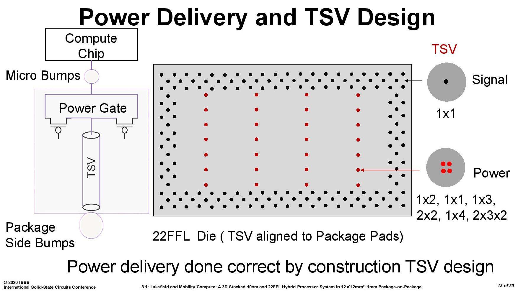
Power supply and design of signal points TSV (through silicon vias)
Base Chip
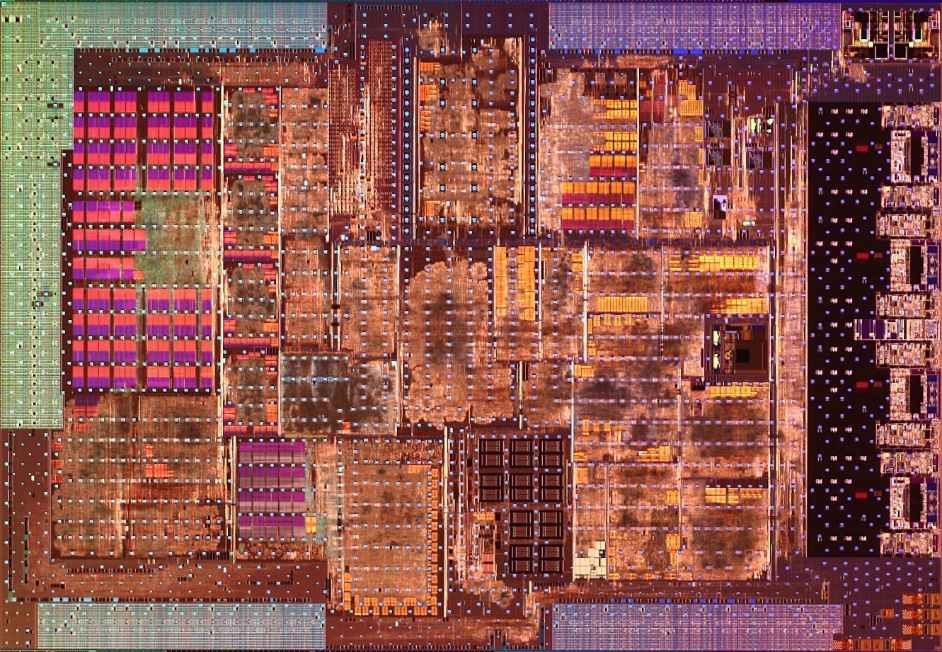
Photo of the bottom base chip
The base chip is much simpler and is manufactured using the 22FFL process technology, which is an optimized version of the 14nm process technology with less stringent restrictions, so that Intel can produce these chips without problems in any quantity, almost without scrap. The main difficulty is the die-to-die connections between the two microcircuits.
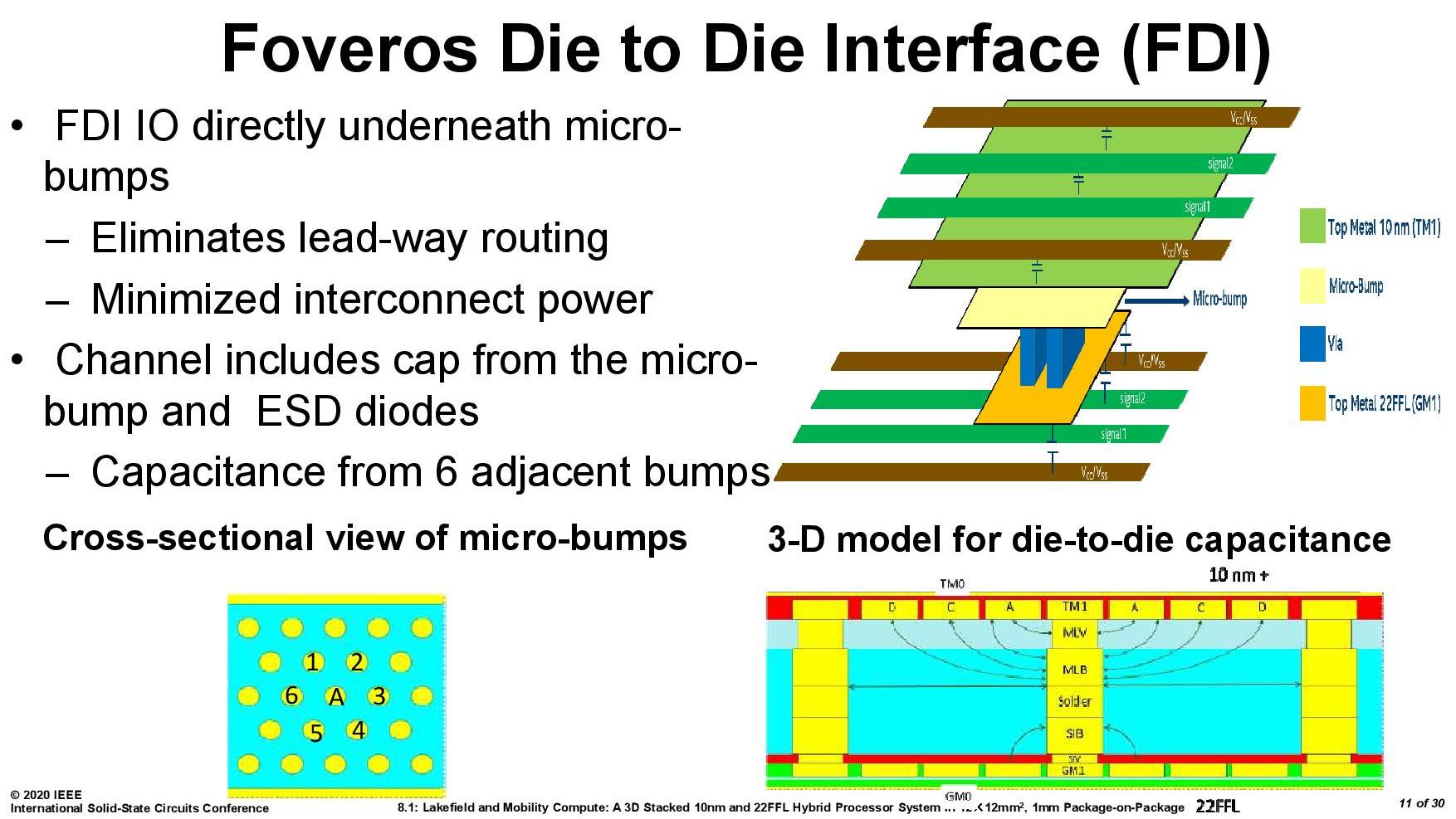
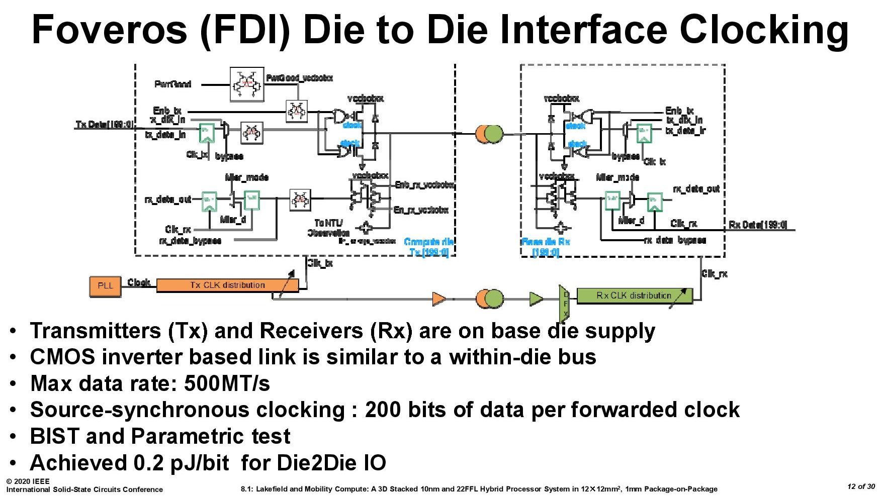
Forevos die-to-die interconnect (FDI) Base Chip
Contents:
- Audio codec
- USB 2.0, USB 3.2 Gen x
- UFS 3.x
- PCIe Gen 3.0
- Touch hub for always-on
- I3C, SDIO, CSE, SPI / I2C
First laptops and tablets
A number of Lakefield laptops and tablets are already in production. Among the early devices ... the
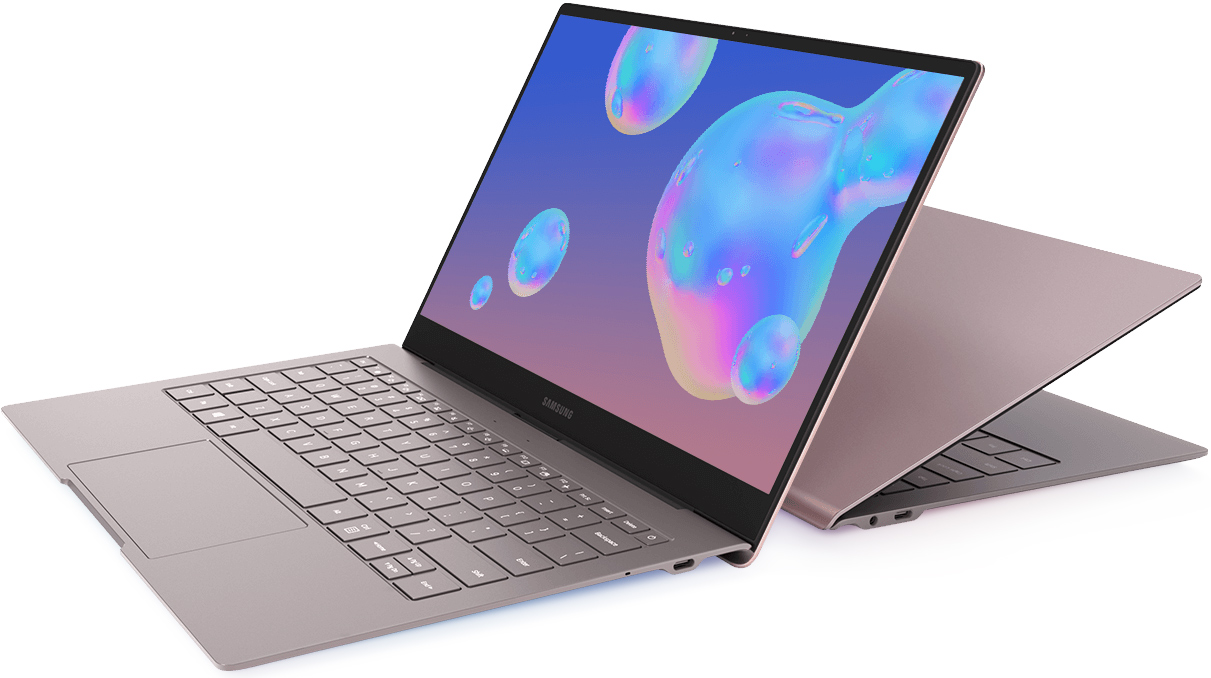
Galaxy Book S (also available on Qualcomm Snapdragon 8cx processors with similar specs), due out in July 2020, the
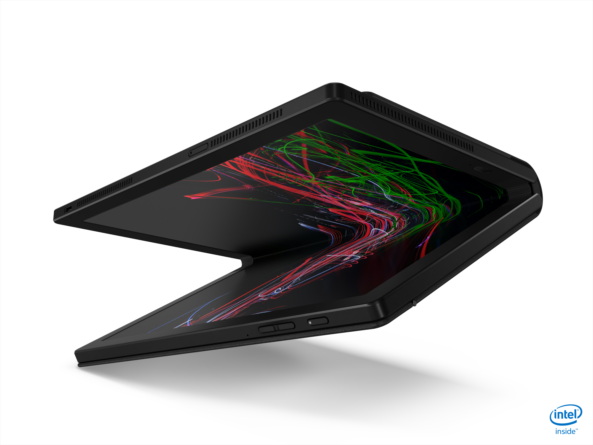
Lenovo ThinkPad X1 Fold foldable tablet laptop with a crazy $ 2,499 price tag for the 1TB version
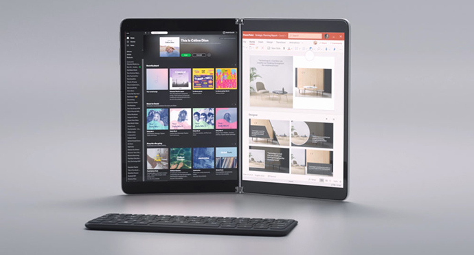
and tablet Microsoft Surface Book Neo, due out closer to winter.
Lakefield future
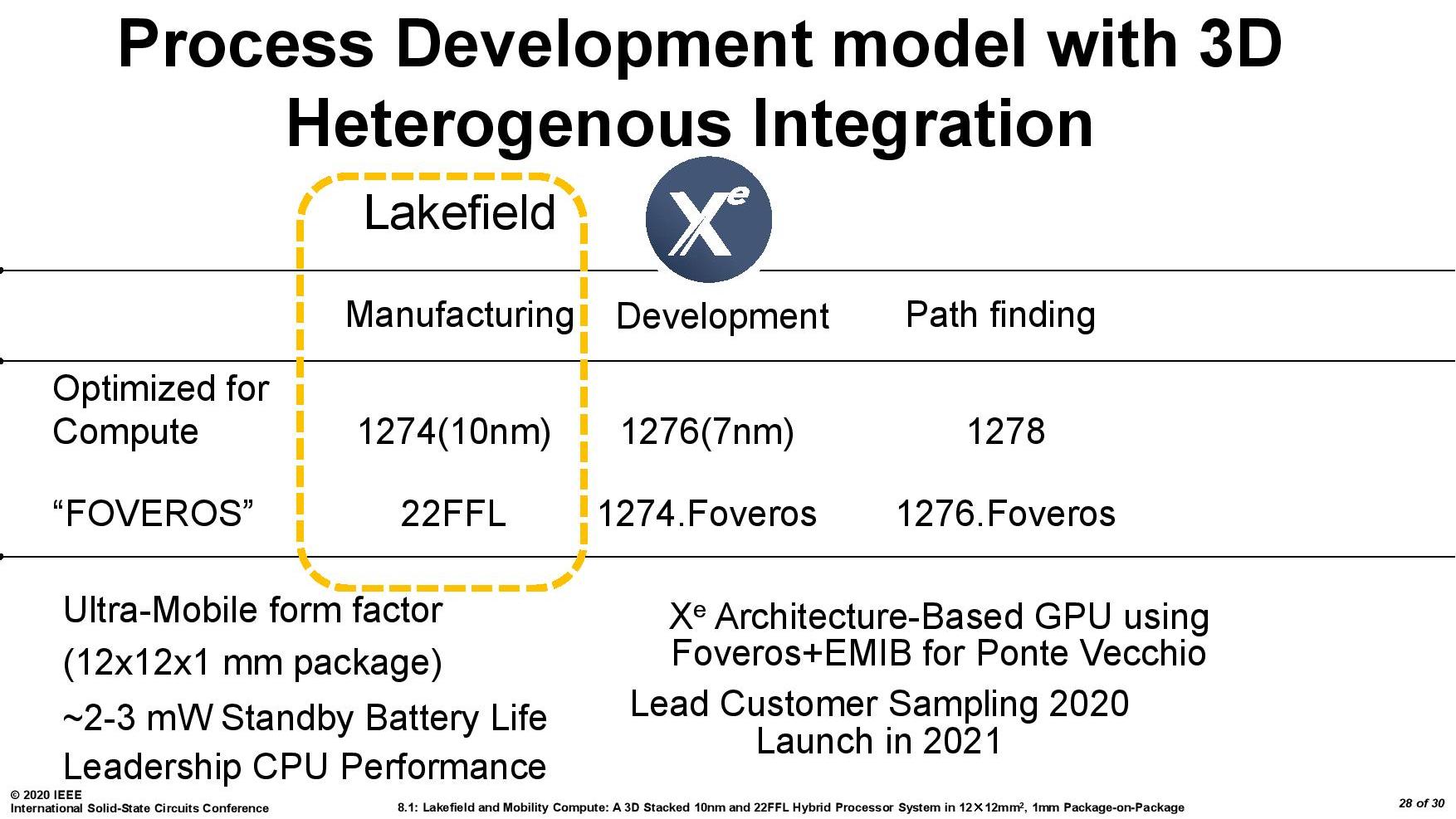
Even if this version of Lakefield doesn't perform well in benchmarks, this is a big step for Intel. Hybrid designs and multi-layer bonding between substrates are featured in Intel's development roadmap. It all depends on how much Intel is willing to experiment and how well it can implement engineering ideas. There have been discussions that Intel may be considering a hybrid 8 + 8 processor design in the future. Nothing is known about this, but a Ponte Vecchio with a multi-layer backing is definitely scheduled for the end of 2021.
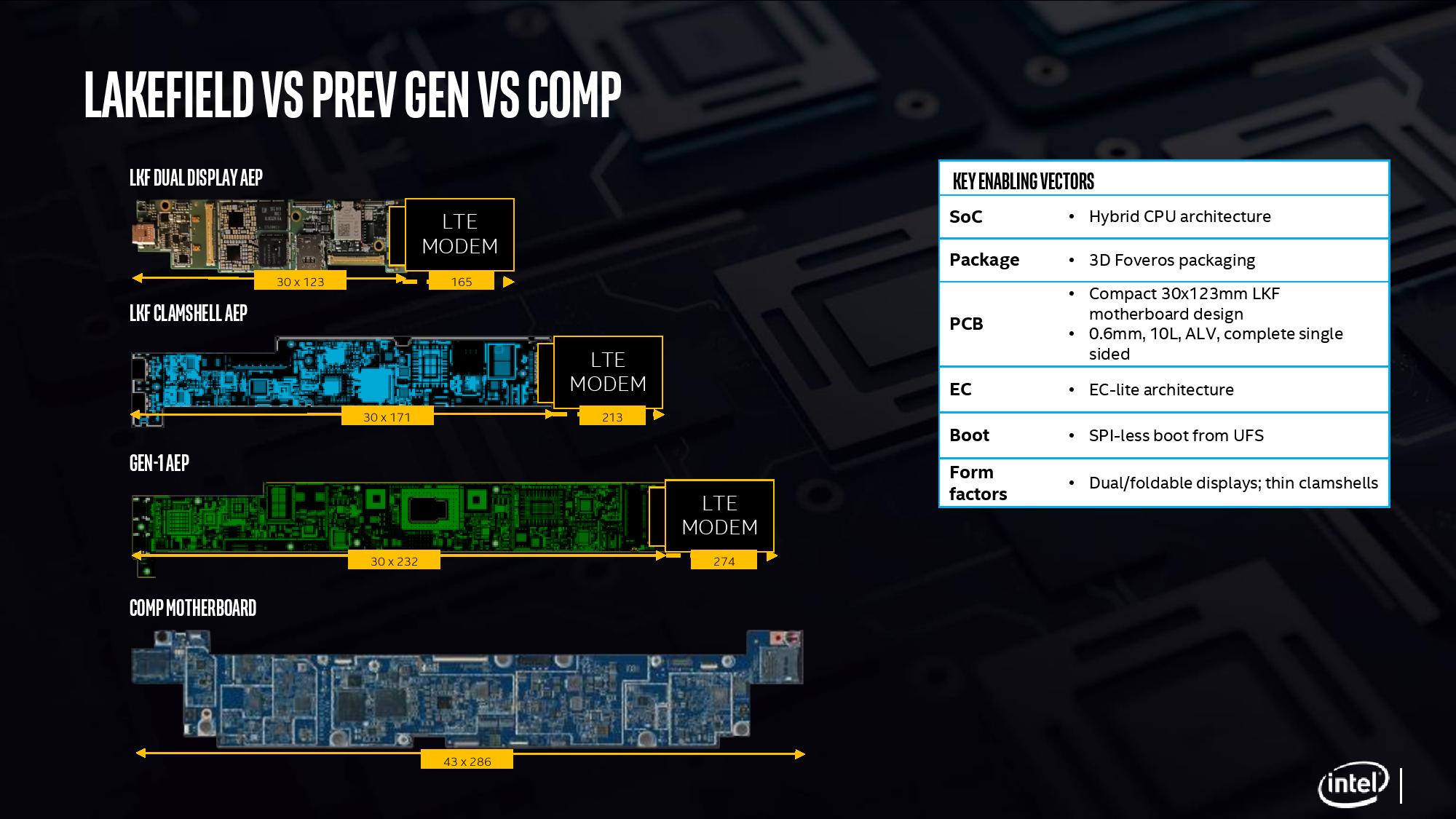
Lakefield motherboard size (30 * 123mm) compared to previous generations motherboards
Perhaps some innovative Intel processors will be released not for desktop computers, but, for example, for cars or 5G networks. Lakefield is essentially a relatively low-performance CPU that will be installed in laptops and tablets, like the Atom processors. It can be said in advance that it will not be easy to compete in this segment, especially with AMD mobile processors and ARM processors like Snapdragon. But the more competition, the better the buyers.